Article

Single-Event Upset Characterization of a Shift Register in 16 nm FinFET Technology

by
Federico D’Aniello
1,*,
Marcello Tettamanti
1,
Syed Adeel Ali Shah
1,
Serena Mattiazzo
2,3,
Stefano Bonaldo
3,4,
Valeria Vadalà
1 and
Andrea Baschirotto
1
1
Department of Physics “G. Occhialini”, University of Milano-Bicocca, Piazza della Scienza 3, 20126 Milano, Italy
2
Department of Physics and Astronomy “Galileo Galilei”, University of Padua, Via F. Marzolo 8, 35131 Padova, Italy
3
INFN Sezione di Padova, Via Marzolo 8, 35131 Padova, Italy
4
Department of Information Engineering, University of Padua, Via G. Gradenigo 6b, 35131 Padova, Italy
*
Author to whom correspondence should be addressed.
Electronics 2025, 14(7), 1421; https://doi.org/10.3390/electronics14071421
Submission received: 19 February 2025 / Revised: 27 March 2025 / Accepted: 27 March 2025 / Published: 31 March 2025

Abstract

:
Today, many electronic circuits are required to be able to work effectively, even in environments exposed to ionizing radiation. This work examines the effects of ionizing radiation on shift registers realized in a bulk 16 nm FinFET technology, focusing on Single-Event Upset (SEU). An SEU occurs when a charged particle ionizes a sensitive node in the circuit, causing a stored bit to flip from one logical state to its opposite. This study estimates the saturation cross-section for the 16 nm FinFET technology and compares it with results from a 28 nm planar CMOS technology. The experiments were conducted at the SIRAD facility of INFN Legnaro Laboratories (Italy). The device under test was irradiated with the ion sources 58 N i and 28 S i , both with different tilt angles, to assess the number of SEUs with different LET and range values. Additionally, the study evaluates the effectiveness of the radiation-hardened by design technique, specifically the Triple Modular Redundancy (TMR), which is a technique commonly employed in planar technologies. However, in this particular case study, TMR proved to be ineffective, and the reasons behind this limitation are analyzed along with potential improvements for future designs.

1. Introduction

Digital electronic circuits, in many applications, must reliably operate under increasingly adverse conditions, such as extremely high or low temperatures, intense electromagnetic disturbances, and high-radiation environments. This is particularly critical for space applications [1], particle physics experiments [2], nuclear power plants, and advanced medical technologies, where devices are often subject to harsh radiation [3]. This work investigates and characterizes the resilience of digital circuits fabricated with a bulk 16 nm FinFET technology to high-ionizing radiation. The insights gained could guide the enhancement of readout circuits for future particle detectors at the Large Hadron Collider (LHC) at CERN, Switzerland.
Ionizing radiation can induce malfunctions in electronic circuits due to the energy transfer during the interaction of radiation particles with semiconductor materials [4,5], leading to the generation of electron–hole pairs. The primary effect responsible for generating an electric current from matter–radiation interaction is charge deposition due to direct or indirect ionization. Direct ionization occurs when ions come into contact with the semiconductor and locally release charge, while indirect ionization results from neutrons and protons generating charge through collisions within the material. Once this charge is injected into the semiconductor, the phenomena of charge transport and collection are imputed to move this charge to the sensitive nodes of electronic devices. When charge collection occurs at the reverse-biased drain junction of a transistor, it induces a transient current pulse, which may change the electrical state of the transistor [6,7].
These faults, collectively known as Single-Event Effects (SEEs), can manifest as either temporary (soft errors) or permanent (hard errors) faults. Hard errors result in irreversible and permanent damage to the device, leading to data loss and potentially failure. Most common examples of hard errors are:
  • Single-Event Latchup (SEL): It happens in CMOS technology where ionizing radiation can activate parasitic bipolar transistors that are structurally intrinsic to this technology. Excessive current flow can permanently damage the device [8].
  • Single-Event Gate Rupture (SEGR): A phenomenon that is particularly critical in devices with thin oxide and it is due to a high-energy particle that can create a localized electric field strong enough to break down the gate oxide of a MOSFET, leading to permanent transistor failure [9].
  • Single-Event Burnout (SEB): This occurs in power devices, such as silicon carbide (SiC) devices, when a particle strike induces a high-current condition, potentially destroying the device due to thermal runaway [10].
In contrast, soft errors occur when the circuit experiences a transient disruption, but its normal behavior can be restored through a reset or by rewriting the affected data. Although not destructive, these errors are particularly critical because, being transient, they are difficult to detect and can compromise data integrity and system reliability, leading to significant system-level errors. Typical examples of soft errors are:
  • Single-Event Upset (SEU): Occurs when a single ionizing particle impacts a logical node, such as a memory cell, a register, or a latch, causing a logic state change and leading to data corruption. The ‘critical charge’ ( Q c r i t ) defines the threshold charge that a circuit node can tolerate without a change in logic state, serving as a key measure of the impact of an SEU [3,4,11].
  • Single-Event Transient (SET): Temporary voltage glitch induced in combinational logic circuits. If this glitch propagates and is latched into a sequential element (e.g., a flip-flop), it may result in an SEU [3].
  • Multiple-Cell Upset (MCU): Occurs when a single radiation event simultaneously affects multiple adjacent memory cells, potentially causing correlated errors that are harder to correct. They are also called Multiple-Bit Upset (MBU) when the affected cells correspond to the bits from the same logical word in the memory [12].
This work focuses on SEUs, which can be prevented or corrected in real-time through proficient design techniques.
To mitigate SEUs, several techniques have been developed [13], including:
  • Rad-Hard By Process (RHBP): consists of the modification of some integrated circuit (IC) manufacturing steps, such as doping levels or layer thicknesses, so that they make the transistor radiation-tolerant. The drawback is a significant increase in the costs due to the custom modification in the production steps [14]. Additionally, radiation hardness can be improved by physical shields which prevent particles from reaching the IC. While effective, this method is expensive and requires a substantially large area on the silicon and/or of the whole system [15,16].
  • Rad-Hard By Design (RHBD): involves the use of special add-on circuits to minimize the possibility of SEU. It is the most widely used method, and its implementation can be off-chip through dedicated software approaches or on-chip using specific circuit structures. Most common techniques are the Triple Modular Redundancy (TMR) that analyze the results of multiple redundant outputs, and the Quatro latch that uses redundant reinforced feedback architectures [3,17,18,19,20]. Moreover, it is possible to enhance the radiation hardness of transistors by using specific layout techniques such as squared gates, guard rings, and triple wells [21].
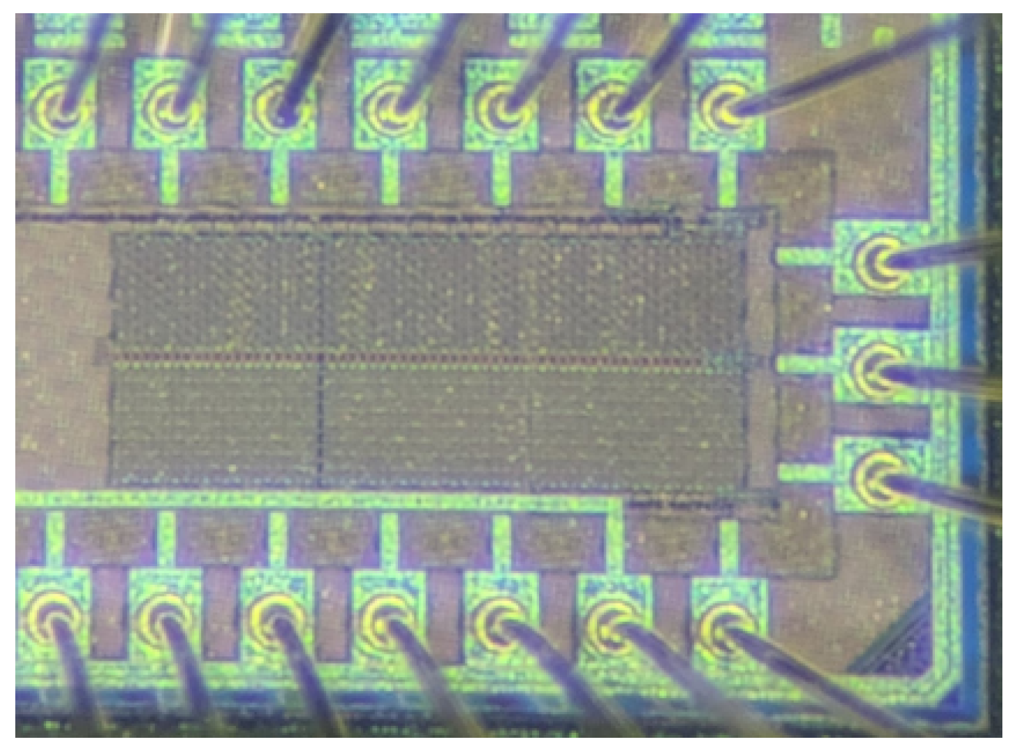
This work investigates the effect of ionizing radiation in terms of SEUs on a digital circuit developed in a silicon 16 nm FinFET bulk technology. The continuing demand for higher integration in modern circuits has forced an increasingly aggressive technology scaling, with FinFETs emerging as the optimal solution for sub-16 nm nodes. Thanks to their unique characteristics and their 3D structure, these technologies offer significant advantages in various fields, including radiative environments such as aerospace. However, for use in radiation-prone environments, a thorough characterization of their radiation robustness is crucial. Although numerous studies have already been conducted, further analysis is essential to fully understand their behavior and ensure their reliability under extreme conditions [22,23,24]. In some studies, FinFETs have shown significantly lower SEU cross-sections compared to planar technologies at low LET values, thanks to their 3D structure, which reduces charge collection [22]. The second goal of this work is the analysis of the effectiveness of RHBD techniques for this technology. In fact, numerous RHBD circuit solutions have proven effective in classical planar CMOS technologies. However, the increasing demand for higher performance and lower power consumption drives the use of FinFET technologies, whose robustness against SEU remains uncertain. Moreover, RHBD techniques from planar technologies may not be directly transferable and valid for FinFET technology, so it is necessary to study which configuration can bring benefits.

2. Proposed Design

To characterize the impact of ionizing radiation on digital logic circuits in 16 nm FinFET technology in terms of SEU, a shift register in a Serial-In Serial-Out (SISO) configuration was selected as the Device Under Test (DUT). In a SISO configuration, data are inserted serially and then read out, allowing any bit-flips along the chain to be observed unambiguously. This simplifies error detection compared to a more complex memory cell, where bit corruption might be more difficult to identify. The disadvantage of this error estimation is the possibility of not recognizing an MBU, but the small number of bits in each register and a fast clock reduce the possibility of MBUs. The shift register consists of a chain of D flip-flops that share the clock signal and the supply voltage, as shown in Figure 1. Figure 2 presents the master–slave configuration of a single memory element (flip-flop). The register, composed of 150 bits, operates at a switching frequency of approximately 5 MHz, which represents an optimal trade-off between performance and power consumption.
The second goal of this research activity is to test the effectiveness of a Rad Hard by Design circuit to possibly reduce and prevent SEUs and, more generally, soft errors for FinFET technology. The technique under investigation is the TMR and consists of using three identical flip-flops for each cell instead of a single flip-flop. A schematic of a TMR cell is shown in Figure 3. The three flip-flops (flip-flop A, flip-flop B, flip-flop C) have the same input data, while the three outputs are sent to an additional circuit named the Majority Voter [25]. Thanks to the logic shown in Figure 4, the Majority Voter can bring its output to the logic level that occurs in the majority among its three inputs (i.e., the three flip-flop outputs). If only one of the three flip-flop outputs was to change due to the impact of a sufficiently charged ionizing particle ( Q > Q c r i t ), the other two would cause the overall output of the Majority Voter to still be correct. The advantage of the proposed circuit is that it uses few transistors and occupies a limited area.
The Majority Voter circuit can be enabled through a multiplexer. In this way, it is possible to test both the chain of 150 simple flip-flops without special rad hard techniques and the chain of 150 TMR cells. A reset signal is also present to restore the initial state of all flip-flops at a logic 0 value. The layout of the TMR register is shown in Figure 5. It is evident that the TMR cell chain occupies a larger area than the simple shift register cell, but nevertheless, this is still relatively moderate compared to other possible RHBD solutions. The single flip-flop occupies an area of 79 μm2, while the single TMR cell occupies 309 μm2. In order not to further accentuate the area utilization, it was chosen not to use a dedicated guard ring for each individual cell, but a single guard ring for the entire register. The area occupied by the entire 150-bit register is therefore 0.047 mm2. A micrograph of the DUT is shown in Figure 6.

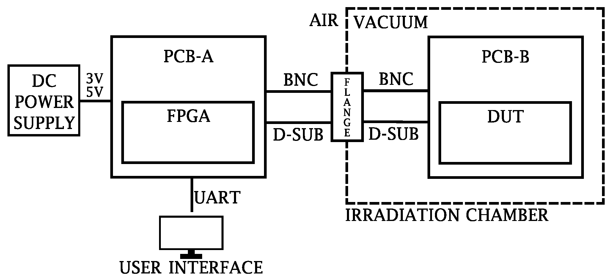
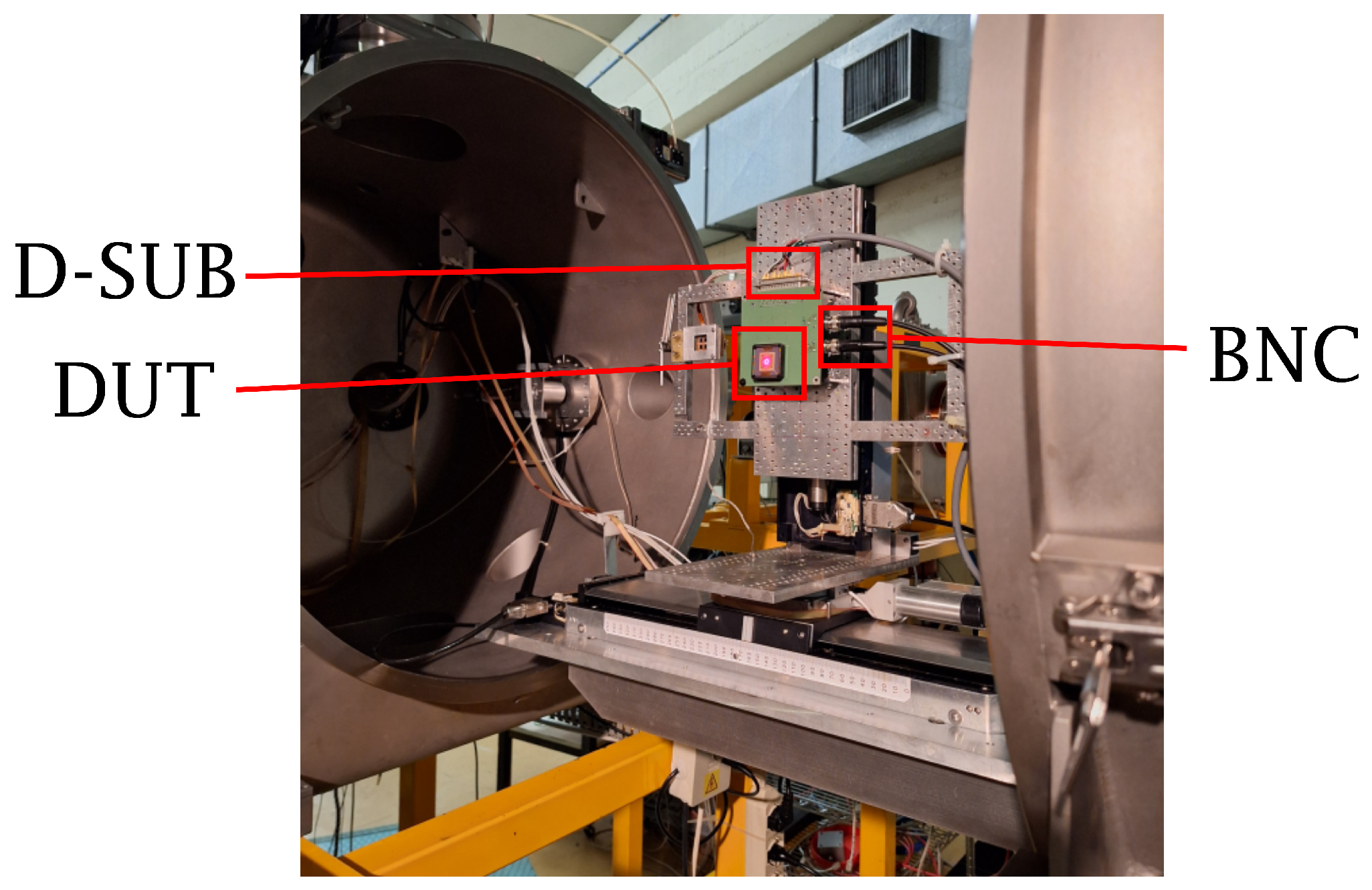
3. SEU Measurement Setup

The proposed integrated circuit has been tested at the SIRAD irradiation facility, which is dedicated to bulk damage and SEE studies in semiconductor devices and electronic circuits. SIRAD is installed at the Tandem XTU accelerator of the INFN Legnaro National Laboratories in Italy [26]. This is an electrostatic Van de Graaff accelerator with a maximum operating voltage of 14 MV; available ion sources go from 1 H (28 MeV) to 197 A u (275 MeV). The beam injected into the SIRAD beamline is extracted at 70° from the main line. Essential elements of the SIRAD line are, in the listed order, a system of adjustable horizontal and vertical slits, a quadrupole doublet for focusing the beam down to millimetric spots, an electric rastering system for irradiating extended targets, an irradiation chamber with a vertical sample-holder, available both for diagnostic and irradiation purposes, a chamber with an extractable Faraday cup, and finally, an irradiation chamber including a battery of small Faraday cups and a battery of silicon PIN diodes with pulse counting electronics [26]. Inside the SIRAD irradiation chamber, vacuum conditions are essential to minimize beam energy loss and unwanted interactions, maximize beam stability, enhance experimental precision, and reduce background noise.
The standard diameter for a focused beam spot is between 3 and 4 mm, and beam diagnostics is conducted using an extractable Faraday Cup situated close to the target area. A visual examination of the beam profile can be carried out on a quartz window located at the end of the irradiation chamber. The rastering system ensures a uniform irradiation with better than 5% precision across a designated area of 5 × 5 cm2 at the target plane. Continuous monitoring of the beam current and its uniformity on the target is facilitated by a grid of 3 × 3 small Faraday cups placed behind the target area. To establish the beam settings, assess the ion flux, verify uniformity, and evaluate beam quality, an array of silicon PIN diodes as particle counters is used. While irradiation occurs, the device being tested is encircled by four diodes for closely monitoring the beam characteristics in real time [27].
The test bench was composed as follows. A first PCB, called PCB-A in Figure 7, was placed outside the irradiation chamber and includes a CMOD S7 FPGA that generates the reference clock through a clock generator from its internal clock of 12 MHz. The FPGA also generates the data stream, the reset signal, and the control signal of the multiplexer. All these signals are sent via a D-SUB cable to a second board, PCB-B in Figure 7, located inside the irradiation chamber and containing the integrated circuit (DUT). Similarly, the clock is transmitted via a BNC cable. The FPGA cannot be placed inside the irradiation chamber due to power dissipation problems in a vacuum. The environment in which the experiment takes place is very noisy because of the numerous instruments connected to the supply line, the length of the connections, and the interconnection flange of the chamber. To reduce the noise, the signals are then converted from single-ended to differential on the PCB-A through amplifiers before being sent out. These are then similarly converted to single-ended again on PCB-B, read by the IC, and sent back to the FPGA. The TMR output of the IC is also sent back to PCB-A. PCB-A also has, in the input, two supply voltages, 5 V and 3 V. The 5 V is needed to supply the amplifiers for single-ended to differential conversion (and vice versa). The 3 V supplies the linear regulator used to generate the 850 mV supply voltage and the two Level Shifters (LSs). The LSs are used to convert the signals from the 3 V to the 850 mV domain (DUT supply voltage). Both 5 V and 850 mV are transmitted again via D-SUB to PCB-B.
The DUT output signals are then received by the FPGA, which reads the data and compares the output data stream with the input data stream. Thanks to the implemented software, the number of SEUs is counted, and the result is saved as a text file. The FPGA is then connected to a terminal via USB, which serves as an interface and enables real-time monitoring.

4. Experimental Results

The measurement setup was first simulated and tested in a safe environment without radiation. No systematic errors occurred in this condition, and the system reported no error detection.
The measurement setup was then installed as described in the previous section in the SIRAD irradiation facility and as shown in Figure 8. Note that only the IC is visible on the test board, while the other discrete components needed for the interfacing are on the back of the board and hence are not visible in the picture. The D-SUB and BNC cables connect PCB-A to PCB-B located outside the radiation chamber.
In order to reconstruct the SEU cross-section curve versus Linear Energy Transfer (LET), different values of LET were chosen, either by changing the ion source or by changing the tilting angle. Even if the SIRAD irradiation facility supports ionic sources from 1 H (28 MeV) to 197 A u (275 MeV), only a subset of these are contained in a single ionic cocktail and can therefore be tested in sequence within a reasonable time. The ionic cocktail, composed of 16 O , 28 S i , 58 N i , 107 A g , was chosen as the source for this experiment. LET, range and energy are reported in Table 1, where the range is the total distance that a charged particle can travel in a material before coming to a stop due to energy loss from interactions with the material itself.
The surface LET and the range in silicon are calculated using the SRIM software (v2013) [28], which takes as input the values of the energies of each individual ion source of the TANDEM facility and it gives the corresponding LET inside silicon. However, the LET will have to be recalculated taking into account the energy loss in the metal and oxide layers present above the silicon active zones. The SRIM software can also provide the LET on the surface of the silicon active area after the attenuation caused by the metal layers. An estimation of the metal layers was made according to the Design Rule Manual of the used technology and added in SRIM. Another way to modify the LET is by changing the angle of incidence of the radiation on the IC. This introduces an angle-dependent factor that affects the LET, as described by the following equation:
L E T e f f = L E T / c o s ( θ )
This provides the possibility to take different measurements at different surface LET values with the same ion and therefore to save a considerable amount of time.
Changing the angle of incidence θ 0 also leads to an inevitable change in the range of the particle in silicon, which can therefore be calculated as:
R A N G E e f f = R A N G E × c o s ( θ )
The reduction in the range should be taken into account when the ion source is chosen. Some ions could have not a range long enough to reach the sensible areas of the MOS transistors. This is especially true for 3D structures (like FinFET) where sensible areas are further away [29].
Due to the limited amount of allocated beamtime, only two ion beams have been selected for the experiment. As the first ion beam, 58 N i was chosen because it has the best trade-off between particle range (typically, it must be >40 µm) and LET, which is expected to be high enough to be in the saturation part of the cross-section curve. In addition, the tilt angle was varied from 0° to 30° or 45° to achieve slight changes in LET and range without changing ion source. When considering the thicknesses and the materials of metals and oxide layers of the technology used, the surface LET value for the 58 N i beam is 29.36 MeVcm2/mg (calculated with TRIM/SRIM). Regarding the LET, 107 A g is also a good option, but the range is probably insufficient to pass through all the metal layers above the sensitive area, particularly for θ 90 °. Also, the 28 S i ion was selected to irradiate the device. The surface LET at 0° (calculated with SRIM, considering the metal layers) is 8.58 MeVcm2/mg. Compared to the previous ion species, LET values for this beam were much lower, even when a tilt angle of 45° was applied. Despite integrating fluence values 10 times higher than for the previous nickel beam, for any bit pattern, any register configuration, and any LET value (different tilting angles), no SEU could be detected. This is an indication that the charge released in a sensitive node with this ion beam was below the critical value and could not induce any SEU. These LET values are, therefore, below the LET threshold value for this device/technology node. Finally, it should be noted that the 16 O ion source was not used, since having a lower LET than 28 S i certainly would not have generated SEUs in an reasonable measurement time, and this value is probably under the threshold LET for this technology [22]. All the surface LETs, ranges, and tilt angles used for the experiment are reported in Table 2.
For all measurements, a minimum fluence of 50 × 10 6 ions/cm2 was used. The ion flux is set and continuously monitored during the irradiation by a set of diodes.
The results obtained with the applied LETs are finally reported in Table 3.
The obtained results are compared with similar measurements collected in the same facility with a shift register developed in bulk 28 nm planar technology [30]. In that case, the saturation cross-section was σ s a t = 2 3 × 10 8 cm2/bit. Compared with this measurement, the 16 nm FinFET technology presents a cross-section lower by an order of magnitude ( 10 8 vs. 10 9 ).
From Table 3, it can be seen that all the measurements with the data pattern “0” have a null cross-section for both the configuration and all the LET values tested. This means that flip-flops have high radiation resistance when the pattern is “0”. The reason could be found in the topology used for the flip-flop (shown in Figure 2) and from the different intrinsic susceptibility of NMOS and PMOS [31,32].
Also, in Table 3, it can be seen that there is no relevant difference in the SEU cross-section of the TMR circuit and the unprotected shift register. The issue may arise from the layout of the three flip-flops within the TMR single cell, which are placed too close together and lack sufficient spacing to ensure complete independence of the elements. Moreover, this effect becomes even more pronounced in scaled technologies, where the sensitive nodes are positioned even closer together. In such conditions, the charge movement induced by ion strikes can interact with multiple transistors simultaneously, significantly increasing the probability of MBU [12]. However, implementing a layout with greater spacing or a dedicated guard ring for each individual cell would have required a significantly larger area, contradicting the trend toward scaling down technologies. An alternative would be to use a different RDBD technique, such as the Quatro latch. Unlike TMR, which relies on physically separated copies, the Quatro latch incorporates internal redundancy by reducing the area and making it particularly suitable for advanced FinFET nodes where physical separation is challenging.

5. Conclusions

This work explores the effects of ionizing radiation with heavy ions on a circuit fabricated in a bulk 16 nm FinFET technology. Measurements conducted at the SIRAD irradiation facility revealed that this FinFET technology demonstrates superior tolerance to SEU compared to a bulk 28 nm planar technology, as indicated by the cross-section that is an order of magnitude lower. However, the complete reconstruction of the cross-section curve was not satisfactorily achieved, highlighting the need for further investigation. An ion source with LET between 10 MeV cm2/mg and 25 MeV cm2/mg may be more recommended for future studies. Additionally, a dependency of radiation resistance on the data-path has been observed, influenced by the circuit topology used. The application of RHBD techniques, specifically the TMR, proved to be less effective for circuits using FinFET technologies than in planar CMOS technologies. In FinFET technologies, devices are highly compact and closely spaced due to aggressive technology scaling (e.g., 16 nm and below). When an ionizing particle impacts the device, it can induce a single event that affects multiple transistors simultaneously. If the three modules of a triple modular redundancy (TMR) system are too close to each other, a single radiation-induced event can damage all three copies, making the TMR ineffective. In addition, the high integration density makes it difficult to implement TMR with sufficient physical separation. It is suggested that future designs include a dedicated guard ring for each TMR element in the layout to mitigate MCU. Special effort is required not to increase the area excessively. Finally, other RDBD techniques, such as the Quatro latch, could be investigated and can potentially improve the shift register robustness to radiation.

Author Contributions

Writing—original draft, F.D. and M.T.; writing—review and editing, F.D., M.T., S.A.A.S., V.V., A.B., S.M. and S.B.; design activity, M.T. and A.B.; design and validation of the measurement setup, M.T., F.D., S.A.A.S. and V.V.; characterization and measurement activity, M.T., F.D., S.A.A.S., S.M. and S.B.; supervision, A.B. All authors have read and agreed to the published version of the manuscript.

Funding

This research received no external funding.

Data Availability Statement

The original contributions presented in this study are included in the article. Further inquiries can be directed to the corresponding author.

Acknowledgments

The authors acknowledge the technical staff of INFN Sezione di Padova and the University of Padua for their support in the measurement activities.

Conflicts of Interest

The authors declare no conflicts of interest.

References

  1. Stassinopoulos, E.; Raymond, J. The space radiation environment for electronics. Proc. IEEE 1988, 76, 1423–1442. [Google Scholar] [CrossRef]
  2. Whitmore, J.; Rivetta, C.; Shenai, A.; Elias, J.E.; Holm, S.; Baumbaugh, A.E.; Knickerbocker, K.; Zimmerman, T.; Ronzhin, A.; Yarema, R.J.; et al. Radiation validation for the CMS HCAL front-end electronics. In Proceedings of the 8th Workshop on Electronics for LHC Experiments, Colmar, France, 9–13 September 2002; pp. 433–438. [Google Scholar] [CrossRef]
  3. de Aguiar, Y.Q.; Wrobel, F.; Autran, J.-L.; Alía, R.G. Single-Event Effects, from Space to Accelerator Environments: Analysis, Prediction and Hardening by Design; Springer: Berlin/Heidelberg, Germany, 2025. [Google Scholar] [CrossRef]
  4. Bettini, A. Introduction to Elementary Particle Physics; Cambridge University Press: Cambridge, UK, 2008. [Google Scholar]
  5. Schwank, J.R.; Shaneyfelt, M.R.; Fleetwood, D.M.; Felix, J.A.; Dodd, P.E.; Paillet, P.; Ferlet-Cavrois, V. Radiation Effects in MOS Oxides. IEEE Trans. Nucl. Sci. 2008, 55, 1833–1853. [Google Scholar] [CrossRef]
  6. Calligaro, C.; Gatti, U. Rad-Hard Semiconductor Memories; River Publisher: Gistrup, Denmark, 2018. [Google Scholar]
  7. Dodd, P.E.; Massengill, L.W. Basic mechanisms and modeling of single-event upset in digital microelectronics. IEEE Trans. Nucl. Sci. 2003, 50, 583–602. [Google Scholar] [CrossRef]
  8. Guagliardo, S.; Wrobel, F.; Aguiar, Y.Q.; Autran, J.-L.; Leroux, P.; Saigné, F.; Pouget, V.; Touboul, A.D. Single-Event Latchup sensitivity: Temperature effects and the role of the collected charge. Microelectron. Reliab. 2021, 119, 114087. [Google Scholar] [CrossRef]
  9. Silvestri, M.; Gerardin, S.; Paccagnella, A.; Ghidini, G. Gate Rupture in Ultra-Thin Gate Oxides Irradiated With Heavy Ions. IEEE Trans. Nucl. Sci. 2009, 56, 1964–1970. [Google Scholar] [CrossRef]
  10. Witulski, A.F.; Ball, D.R.; Galloway, K.F.; Javanainen, A.; Lauenstein, J.-M.; Sternberg, A.L.; Schrimpf, R.D. Single-Event Burnout Mechanisms in SiC Power MOSFETs. IEEE Trans. Nucl. Sci. 2018, 65, 1951–1955. [Google Scholar] [CrossRef]
  11. Wang, F.; Agrawal, V.D. Single Event Upset: An Embedded Tutorial. In Proceedings of the 21st International Conference on VLSI Design (VLSID 2008), Hyderabad, India, 4–8 January 2008; pp. 429–434. [Google Scholar] [CrossRef]
  12. Borghello, G.; Ceresa, D.; Pejašinović, R.; Diaz, F.P.; Bergamin, G.; Kloukinas, K. Single Event Effects Characterization of a Commercial 28 nm CMOS Technology. In Proceedings of the TWEPP 2018 Topical Workshop on Electronics for Particle Physics, Geremeas, Italy, 1–6 October 2023; Available online: https://indico.cern.ch/event/1255624/contributions/5443894/ (accessed on 1 December 2024).
  13. European Cooperation for Space Standardization (ECSS) Report. Engineering Techniques for Radiation Effects Mitigation in ASICs and FPGAs Handbook—ECSS-E-HB-20-40A. Available online: https://ecss.nl/home/ecss-e-hb-20-40a-engineering-techniques-for-radiation-effects-mitigation-in-asics-and-fpgas-handbook/ (accessed on 1 December 2024).
  14. Gonzalez-Velo, Y.; Mahmud, A.; Chen, W.; Taggart, J.L.; Barnaby, H.J.; Kozicki, M.N.; Ailavajhala, M.; Holbert, K.E.; Mitkova, M. Radiation Hardening by Process of CBRAM Resistance Switching Cells. IEEE Trans. Nucl. Sci. 2016, 63, 2145–2151. [Google Scholar] [CrossRef]
  15. Millward, D.; Strobel, D. The effectiveness of Rad-Pak ICs for space-radiation hardening. In Proceedings of the 40th Conference Proceedings on Electronic Components and Technology, Las Vegas, NV, USA, 20–23 May 1990; Volume 2, pp. 913–916. [Google Scholar] [CrossRef]
  16. Tang, L.; Wan, C.; Sun, X.; Zhang, M.; Ye, W. Research on Anti-Radiation Hardening Technology of Packaging. In Proceedings of the 2022 23rd International Conference on Electronic Packaging Technology (ICEPT), Dalian, China, 10–13 August 2022; pp. 1–4. [Google Scholar] [CrossRef]
  17. Dang, L.D.T.; Kang, M.; Kim, J.; Chang, I.-J. Studying the Variation Effects of Radiation Hardened Quatro SRAM Bit-Cell. IEEE Trans. Nucl. Sci. 2016, 63, 2399–2401. [Google Scholar] [CrossRef]
  18. Chong, K.-S.; Lwin, N.K.Z.; Shu, W.; Chang, J.S. Radiation-Hardened-by-Design (RHBD) Digital Design Approaches: A Case Study on an 8051 Microcontroller. In Proceedings of the 2020 IEEE International Symposium on Circuits and Systems (ISCAS), Seville, Spain, 10–21 October 2020; pp. 1–5. [Google Scholar] [CrossRef]
  19. Nicolaidis, M. Design for soft error mitigation. IEEE Trans. Device Mater. Reliab. 2005, 5, 405–418. [Google Scholar] [CrossRef]
  20. Li, Y.-Q.; Wang, H.-B.; Liu, R.; Chen, L.; Nofal, I.; Shi, S.-T.; He, A.-L.; Guo, G.; Baeg, S.H.; Wen, S.-J.; et al. A Quatro-Based 65-nm Flip-Flop Circuit for Soft-Error Resilience. IEEE Trans. Nucl. Sci. 2017, 64, 1554–1561. [Google Scholar] [CrossRef]
  21. Wang, H.; Dai, X.; Ibrahim, Y.M.Y.; Sun, H.; Nofal, I.; Cai, L.; Guo, G.; Shen, Z.; Chen, L. A Layout-Based Rad-Hard DICE Flip-Flop Design. J. Electron. Test. 2019, 35, 111–117. [Google Scholar] [CrossRef]
  22. Nsengiyumva, P.; Ball, D.R.; Kauppila, J.S.; Tam, N.; McCurdy, M.; Holman, W.T.; Alles, M.L.; Bhuva, B.L.; Massengill, L.W. A Comparison of the SEU Response of Planar and FinFET D Flip-Flops at Advanced Technology Nodes. IEEE Trans. Nucl. Sci. 2016, 63, 266–272. [Google Scholar] [CrossRef]
  23. Shida, W.; Min, T.; Hongwei, Z.; Bo, M.; Yi, S. Evaluation of Single-Event Upset in FinFET Device. In Proceedings of the 2023 5th International Conference on Radiation Effects of Electronic Devices (ICREED), Kunming, China, 24–27 May 2023; pp. 1–7. [Google Scholar] [CrossRef]
  24. Chi, Y.; Wu, Z.; Huang, P.; Sun, Q.; Liang, B.; Zhao, Z. Characterization of single-event transients induced by high LET heavy ions in 16 nm bulk FinFET inverter chains. Microelectron. Reliab. 2022, 130, 114490. [Google Scholar] [CrossRef]
  25. Danilov, I.A.; Gorbunov, M.S.; Antonov, A.A. SET Tolerance of 65 nm CMOS Majority Voters: A Comparative Study. IEEE Trans. Nucl. Sci. 2014, 61, 1597–1602. [Google Scholar] [CrossRef]
  26. Wyss, J.; Bisello, D.; Pantano, D. SIRAD: An irradiation facility at the LNL Tandem accelerator for radiation damage studies on semiconductor detectors and electronic devices and systems. Nucl. Instruments Methods Phys. Res. Sect. A Accel. Spectrometers Detect. Assoc. Equip. 2001, 462, 426–434. [Google Scholar] [CrossRef]
  27. Silvestrin, L. Characterization of Electronic Circuits with the SIRAD IEEM: Developments and First Results. Ph.D. Thesis, Physics, University of Padua, Padua, Italy, 2011. Available online: https://www.research.unipd.it/handle/11577/3421637 (accessed on 1 December 2024).
  28. Ziegler, J.F. SRIM-2003. Nucl. Instruments Methods Phys. Res. Sect. B Beam Interact. Mater. Atoms. 2004, 219–220, 1027–1036. [Google Scholar] [CrossRef]
  29. Nsengiyumva, P.; Massengill, L.W.; Alles, M.L.; Bhuva, B.L.; Ball, D.R.; Kauppila, J.S.; Haeffner, T.D.; Holman, W.T.; Reed, R.A. Analysis of Bulk FinFET Structural Effects on Single-Event Cross Sections. IEEE Trans. Nucl. Sci. 2017, 64, 441–448. [Google Scholar] [CrossRef]
  30. Mattiazzo, S.; Bonaldo, S.; Matteis, M.D.; Fary, F.; Pipino, A.; Resta, F.; Baschirotto, A. 28 nm High-k Bulk Digital Circuit Performance (SEU) After Heavy Ion Exposure. In TWEPP 2018 Topical Workshop on Electronics for Particle Physics. 2018. Available online: https://indico.cern.ch/event/697988/contributions/3055934/ (accessed on 1 December 2024).
  31. Sun, Q.; Guo, Y.; Liang, B.; Tao, M.; Chi, Y.; Huang, P.; Wu, Z.; Luo, D.; Chen, J. Higher NMOS Single Event Transient Susceptibility Compared to PMOS in Sub-20nm Bulk FinFET. IEEE Electron. Device Lett. 2023, 44, 1712–1715. [Google Scholar] [CrossRef]
  32. Yoshida, K.; Nakajima, R.; Sugitani, S.; Ito, T.; Furuta, J.; Kobayashi, K. SEU Sensitivity of PMOS and NMOS Transistors in a 65 nm Bulk Process by α-Particle Irradiation. In Proceedings of the 2023 International Conference on IC Design and Technology (ICICDT), Tokyo, Japan, 25–28 September 2023; pp. 72–75. [Google Scholar] [CrossRef]
Figure 1. Block scheme of the SISO shift register.
Electronics 14 01421 g001
Figure 2. Master–slave flip-flop schematic.
Electronics 14 01421 g002
Figure 3. Block scheme of a TMR cell.
Electronics 14 01421 g003
Figure 4. Majority Voter logic circuit.
Electronics 14 01421 g004
Figure 5. TMR register layout.
Electronics 14 01421 g005
Figure 6. Micrograph of the DUT.
Electronics 14 01421 g006
Figure 7. Measurement setup.
Electronics 14 01421 g007
Figure 8. Picture of the measurement setup at SIRAD irradiation facility.
Electronics 14 01421 g008
Table 1. Available ion sources.
Ion SourceEnergy [MeV]LET [ MeVcm 2 mg ] Range [µm]
16 O 1083.16107
28 S i 1578.961
58 N i 22030.6837
107 A g 26658.429
Table 2. Applied LETs.
Ion SourceTilt AngleLET [ MeVcm 2 mg ] Range [µm]
58 N i 29.3637
58 N i 30°33.932
28 S i 8.759.32
28 S i 45°12.3141.9
Table 3. Experimental results for TMR and standard register at different LETs.
Ion
Source
Tilt
Angle
LET
[ MeVcm 2 mg ]
DataConfig.Fluence
[ ion cm 2 ]
Nr. of
SEU a
Cross-
Section
per Bit
[cm2]
28 S i 8.71TMR2.00 × 10 8 00
28 S i 45°12.311TMR3.71 × 10 8 00
58 N i 29.361TMR9.84 × 10 7 211.42 × 10 9
58 N i 30°33.91TMR5.44 × 10 7 161.96 × 10 9
58 N i 29.360TMR5.51 × 10 7 00
28 S i 45°12.311Standard8.73 × 10 8 00
58 N i 29.361Standard5.53 × 10 7 101.21 × 10 9
58 N i 30°33.91Standard6.03 × 10 7 91.17 × 10 9
58 N i 29.360Standard1.35 × 10 8 00
a Number of Single-Event Upset.
Disclaimer/Publisher’s Note: The statements, opinions and data contained in all publications are solely those of the individual author(s) and contributor(s) and not of MDPI and/or the editor(s). MDPI and/or the editor(s) disclaim responsibility for any injury to people or property resulting from any ideas, methods, instructions or products referred to in the content.

