You are currently viewing a new version of our website. To view the old version click .
Electronics
  • Article
  • Open Access

24 November 2025

A Low-Complexity Hybrid Phase Shifter Network with Shared-Control Voltage for High-Scan-Gain Phased Arrays

,
,
and
1
School of Physics, University of Electronic Science and Technology of China, Chengdu 611731, China
2
Science and Technology on Space Physic Laboratory, China Academy of Launch Vehicle Technology, Beijing 100076, China
*
Author to whom correspondence should be addressed.

Abstract

This article presents a low-complexity hybrid phase shifter network (PSN) with a shared-control voltage architecture for high-gain phased arrays. The proposed system integrates a 1-bit reconfigurable antenna and a voltage-controlled phase shifter in each channel, achieving continuous 360° phase tuning with low insertion loss (below−1.2 dB) and small amplitude fluctuation (±0.2 dB). A single analog control voltage, distributed through reconfigurable passive resistor dividers, replaces per-channel bias sources, significantly reducing hardware complexity. A genetic algorithm is employed to optimize division ratio vectors for beam steering across a wide angular range while enhancing main-lobe gain. Simulation and experimental results show that compared with a conventional 1-bit PSN, the proposed architecture achieved up to 3.6 dB main-lobe gain enhancement while requiring only two additional control lines. This design offers an effective trade-off between performance and implementation cost for large-scale phased array systems.

1. Introduction

Phased arrays enable beamforming and rapid beam scanning through precise control of the signal phase radiated by each array element []. Due to these capabilities, they have been widely used in wireless communications [], radar systems [], and wireless power transfer []. In such systems, key performance indicators such as scanning gain and sidelobe level (SLL) largely depend on the architecture and implementation of the phase shifter network (PSN) []. Depending on where phase control is implemented within the signal chain, PSNs can be categorized into local oscillator (LO), intermediate frequency (IF), and radio frequency (RF) phase shifter networks [].
In the LO PSN, phase control is applied in the LO path and transferred to the RF signal through mixing, thereby enabling beam steering [,,]. A self-adaptive beam-scanning architecture based on a DDS-PLL structure and angle-of-arrival (AoA) estimation was reported in [], where the phase adjustment was performed in the local oscillator (LO) path to enable real-time beam control. The IF PSN performs phase adjustment at a lower intermediate frequency before upconverting the signal to RF [,]. The relatively low IF frequency simplifies the implementation of phase control []. In contrast, the RF PSN directly applies phase control to the RF signal path without requiring an additional LO distribution network []. This architecture is compact and low-cost, making it especially suitable for large-scale phased array systems. Consequently, it is the most widely adopted in practice [,].
Among various RF phase shifters, electronic phase shifters controlled by electrical signals are the most widely used due to their compact size, low cost, and high integration capability []. Based on their operating mechanisms, electronic phase shifters can be classified into switched-type or reflective-type [,]. A switched-type phase shifter typically realizes quantized phase shifts through switched delay lines of discrete electrical lengths [] or switched filter networks consisting of high-pass and low-pass branches []. However, achieving finer phase resolution (i.e., more bits) requires additional delay or filter branches and switches. Consequently, the number of control lines increases with bit resolution, leading to higher control circuit complexity []. A reflective-type phase shifter achieves continuous phase tuning by controlling the impedance of reflective loads using analog voltages []. Nevertheless, conventional single-voltage-controlled reflective structures exhibit a trade-off between phase tuning range and insertion-loss flatness []. Fluctuations in insertion loss across phase states lead to amplitude mismatches among array elements, thereby degrading beam-scanning performance []. Therefore, achieving a wide continuous phase tuning range while maintaining low insertion loss and amplitude consistency remains a key challenge in RF phase shifter design.
To address this issue, several improved reflective-type topologies based on C–L–C π-type networks have been reported [,], which enhance amplitude flatness and extend the phase tuning range. However, these designs typically require multiple independent bias voltages, increasing hardware complexity. Recently, hybrid phase shifters, which combine discrete coarse tuning with continuous fine tuning, have attracted considerable attention. By leveraging the cooperation between discrete and continuous phase-shift units, hybrid shifters can achieve wide phase coverage and stable insertion-loss characteristics [,,]. Nonetheless, when implemented in large-scale phased arrays, these architectures still require multiple independent bias voltages, resulting in complex control networks and limited scalability.
To overcome these limitations, this work proposes a low-complexity RF hybrid phase shifter network architecture with shared control voltage. Each channel integrates a 1-bit reconfigurable antenna and a cascaded voltage-controlled phase shifter, enabling full 360° phase control with insertion loss below −1.2 dB and insertion-loss fluctuation within ±0.2 dB. Compared with switched-type and reflective-type phase shifters, the proposed design exhibits low insertion loss and minimal amplitude fluctuation. Furthermore, a reconfigurable passive resistive voltage-divider network is introduced to provide a unified reference bias voltage for the entire array, reducing the number of control lines from 2N in conventional designs to N + 2. Unlike conventional hybrid phase shifters, this approach eliminates the need for independent voltage sources for each channel. An eight-element prototype array based on the proposed method was fabricated and experimentally verified at 915 MHz. Compared with a traditional 1-bit array, the proposed architecture improves scanning gain by up to 3.6 dB and effectively suppresses sidelobes, while requiring only two additional control lines. This work introduces a new design concept for developing low-complexity, high scanning gain phased array systems, which can be widely applied in wireless power transfer and related fields.
The remainder of this paper is organized as follows. Section 2 introduces the proposed RF hybrid architecture and shared-bias control circuit. Section 3 presents the performance analysis and GA-based optimization. Section 4 describes the reconfigurable 1-bit element design, Section 5 discusses the measurement results, and Section 6 concludes the paper.

2. Design and Implementation of a Hybrid PSN with Shared-Control Voltage

2.1. System Overview

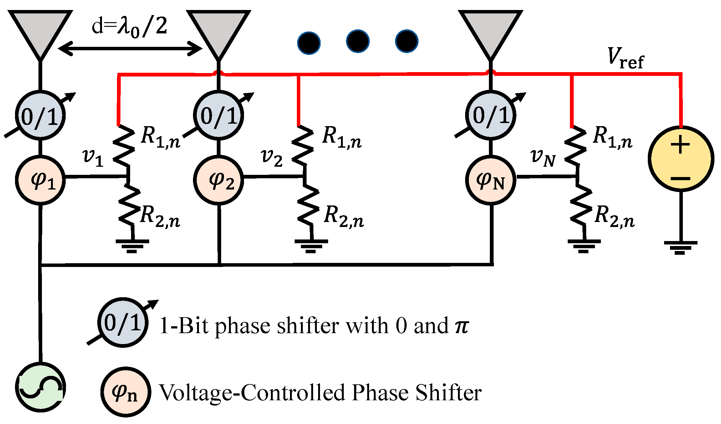
Figure 1 shows the block diagram of the proposed 1 × N linear phased array, which is designed to balance beamforming performance and the control complexity of the PSN. The array comprises N uniformly spaced elements with a half-wavelength ( λ 0 / 2 .) inter-element spacing. Each channel integrates a 1-bit reconfigurable antenna, cascaded with a voltage-controlled phase shifter that is driven by a shared control voltage distributed through passive resistor dividers. This shared-voltage scheme eliminates the need for independent biasing circuits in each channel, thereby significantly reducing control complexity. The hybrid configuration combines the advantages of discrete and continuous phase shifters, enabling continuous 0–360° phase control while achieving a maximum insertion loss of −1 dB and an insertion loss fluctuation within ±0.2 dB.
Figure 1. Block diagram of a hybrid PSN-based phased array with a shared-control voltage scheme.
Table 1 compares the performance of the proposed hybrid architecture with two representative commercial phase shifters. The HMC936 is a digital phase shifter that provides full 360° tuning but requires 6 control lines, with a maximum insertion loss of −5 dB and an insertion loss fluctuation of ±1 dB. The SPHSA-152 is an analog phase shifter that uses only one control line but exhibits a maximum insertion loss of −3.8 dB and an insertion-loss fluctuation of ±1 dB. In contrast, the hybrid architecture uses only two control lines, significantly simplifying the control circuitry while maintaining a lower maximum insertion loss of −1.2 dB and a smaller fluctuation of ±0.2 dB, which is beneficial for beamforming and sidelobe suppression in array applications.
Table 1. Comparison of representative commercial phase shifters operating at 915 MHz.
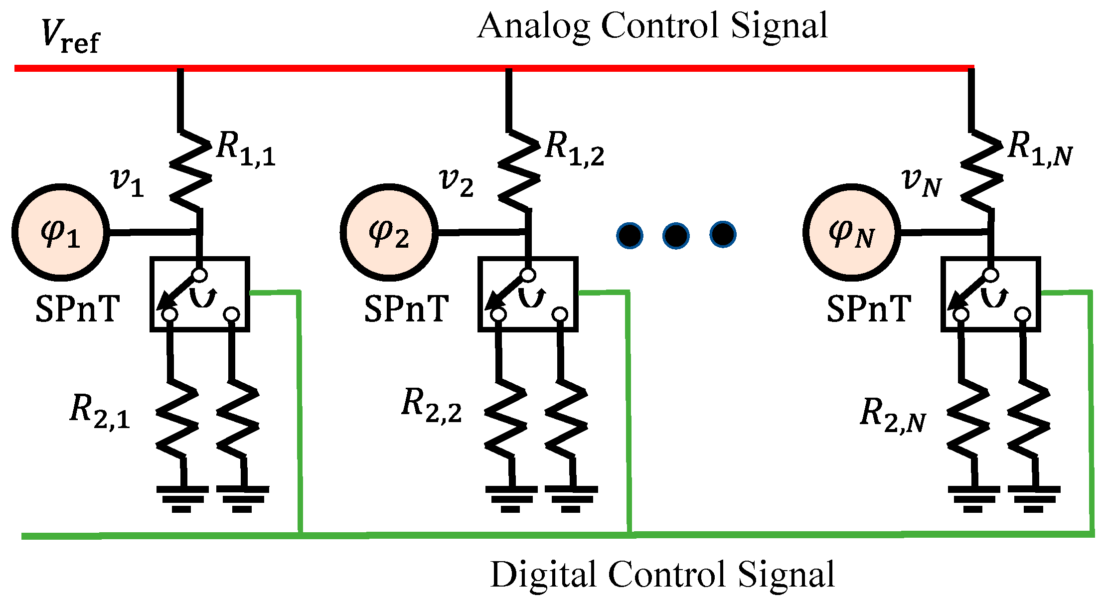
To further reduce the hardware complexity of the proposed hybrid phase shifter architecture, all analog phase shifters are driven by a shared control voltage, V r e f . In each channel, the local control voltage, V n , is generated through a passive resistor divider network consisting of R 1 , n and R 2 , n , expressed as:
V n = k n V r e f
where
k n = R 2 , n R 1 , n + R 2 , n
By selecting an appropriate value for V r e f , the phase distribution across the array is tailored to approximate the ideal phase profile required for beam steering. This shared control voltage approach eliminates the need for independent control voltages for each channel, effectively simplifying the control circuitry.

2.2. System Performance Analysis

Accurate phase control is critical for optimal beamforming performance in phased array systems. In the proposed design, a shared control voltage V r e f and passive resistor dividers are used to simplify the control circuitry. However, this approach introduces phase approximation errors across channels, which may degrade beam steering accuracy.
To quantitatively evaluate the impact of phase errors, the ideal excitation phase Ø i d , n required at the n-th element for beam steering towards a target angle Ø 0 is given by []:
Ø i d , n = k 0 · d · sin θ 0 · n 1 ,   n = 1 , 2 , , N
where k 0 = 2 π / λ 0 represents the wavenumber in free space, and d is the inter-element spacing.
In the proposed design, the actual excitation phase Ø r e a , n at the n-th array element is determined jointly by the discrete and continuous phase shifters. The voltage-controlled phase shifter Ø a n a , n is continuously tunable and depends on the division ratio k n and the shared control voltage V r e f . The 1-bit reconfigurable antenna introduces a discrete phase Ø d i g , n ϵ 0 , π , which is selected based on the phase discrepancy between the ideal phase and Ø a n a , n , according to:
Ø d i g , n = 0 ,     π 2 Ø i d , n Ø a n a , n 3 π 2 π , π 2 < Ø i d , n Ø a n a , n < π 2 .
The actual excitation phase Ø r e a , n is then given by:
Ø r e a , n = Ø a n a , n + Ø d i g , n
To assess the impact of phase errors on array performance, we introduce the Phase Accuracy Efficiency (PAE) metric, defined as:
η P A E θ 0 = n = 1 N e j · Ø r e a , n θ 0 Ø i d , n θ 0 2 n = 1 N e j · Ø i d , n θ 0 Ø i d , n θ 0 2
A PAE value close to unity indicates that the main-lobe gain of the proposed system closely approximates that of an ideal phased array with continuous phase control, thereby confirming its beamforming accuracy.
In addition to main beam gain, side-lobe level (SLL) is a critical metric for evaluating the overall quality of the array radiation pattern. Poor sidelobe suppression not only degrades beam directivity but may also cause electromagnetic interference to adjacent systems or unintended receivers. The SLL, expressed in decibels (dB), is defined as:
S L L = 20   log 10 M a x   m a i n l o b e   l e v e l M a x   s i d e l o b e   l e v e l

2.3. Design of the Hybrid PSN with a Shared-Control Voltage Scheme

In the proposed phased array, the voltage-controlled phase shifter for the n-th channel is expressed as:
Ø a n a , n = f v n = f R 2 , n R 1 , n + R 2 , n V r e f = f k n V r e f
where f · represents the nonlinear mapping between the control voltage and the phase shift, as defined by the voltage-controlled phase shifter’s characteristic.
To enhance beam steering range and phase control resolution, a digital switching mechanism is introduced, as shown in Figure 2. Specifically, each fixed resistor is replaced with a bank of selectable resistors controlled by Single-Pole-n-Throw (SPnT) switches. All SPnT switches are driven through shared digital control lines, enabling synchronous switching across all channels. In the basic configuration, the division-ratio vector k = k 1 , k 2 , k N remains fixed. However, with the shared digital control lines, multiple division-ratio vectors k g = k 1 g , k 2 g , , k N g can be selected, where g 1 , 2 , , G represents different configuration states.
Figure 2. Reconfigurable resistor divider network.
The design objective is to determine the optimal set of division ratios k g g = 1 G that maximizes the sum of η P A E across a specified set of beam steering angles while ensuring that the SLL remains below a predefined threshold S L L t a r g e t . The optimization problem is formulated as:
O b j e c t i v e = max k g g = 1 G θ ϵ Θ max 1 , , G η P A E θ , k g s u b j e c t   t o : S L L θ ,   k g * S L L t a r g e t g * = a r g max g 1 , , g η P A E θ , k g ,   θ ϵ Θ
where Θ = { θ 1 , θ 2 , , θ M } denotes the set of target steering angles, and G is the number of available division ratio vectors. For each steering angle θ m the optimization process selects the configuration index g * that maximizes η P A E while satisfying the sidelobe constraint.
Because this problem is nonlinear and lacks a closed-form analytical solution, a genetic algorithm (GA) [] is employed to obtain a near-optimal solution. The detailed GA optimization framework is presented in Table 2.
Table 2. GA-based Optimization Framework.
It is worth noting that the reconfigurable resistor divider network operates only in the low-frequency control path. Since no RF signal passes through this network, it introduces negligible power loss and does not affect the RF signal path. Unlike conventional hybrid phase shifters, this approach eliminates the need for independent voltage sources in each channel. Although several passive components are added for voltage division, the overall control complexity remains significantly lower than that of conventional per-channel biasing architectures.

3. Numerical Results and Performance Evaluation

To assess the effectiveness of the proposed shared-control hybrid PSN, a numerical simulation was performed on a linear phased array consisting of N = 8 elements with half-wavelength spacing using MATLAB R2023a.
Following the GA-based optimization process described in Section 2.3, two division ratio vectors (i.e., G = 2) were selected for implementation, denoted as k 1 and k 2 . The detailed division ratio k n g for each element n = 1 , 2 , 3 , , 8 and each configuration g 1 , 2 are summarized in Table 3. These values are used to generate the corresponding local control voltages v n = k n g V r e f , which determine the analog phase responses of each channel. The simulation assumes an operating frequency of 915 MHz. The reference control voltage V r e f   was adjusted from 0 V to 15 V to cover the full phase-tuning range of the JSPHS-1000 phase shifter. This voltage range lies well within the device’s rated operating limit of 18 V. Since the control port of the JSPHS-1000 presents a high input impedance, the bias current is extremely small (<1 mA), and the resulting control-line power consumption is negligible. Therefore, the applied voltage range does not compromise the overall low-power characteristic of the proposed system. Beam steering is evaluated across a scan range from 60 ° to 60 ° , with a step size of 1 ° .
Table 3. The division ratio vectors under g = 1 , 2 .
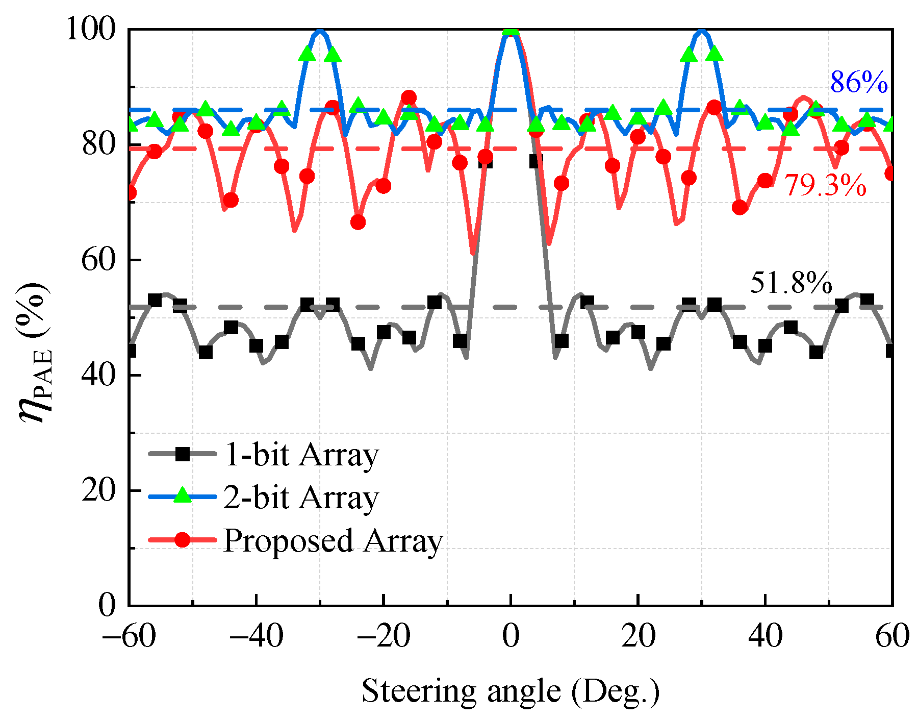
Figure 3 illustrates the simulated η P A E of the 1-bit, 2-bit, and proposed hybrid PSN-based phased array as a function of the beam-steering angle. The 1-bit array shows a pronounced efficiency degradation at large steering angles, whereas the 2-bit array maintains high η P A E across most directions. The proposed design exhibits an efficiency profile closely comparable to that of the 2-bit array throughout the ± 60 ° , sustaining stable performance even under wide-angle steering. The average η P A E values of the 1-bit, 2-bit, and proposed array were 51.8%, 86%, and 79.3%, respectively. Compared with the 1-bit array, the 2-bit and proposed arrays improved the average η P A E by 66% and 53%, respectively. The small difference in improvement demonstrates that the proposed array achieves near 2-bit efficiency while requiring substantially fewer control resources. When the steering angle approaches 0 ° , the phase difference between adjacent elements becomes small, so quantization errors accumulate weakly across the array and have only a minor impact on η P A E However, as the beam is steered toward larger angles, the coarse quantization of the 1-bit array causes a significant efficiency degradation, whereas the proposed method maintains a high η P A E comparable to that of the 2-bit array.
Figure 3. Simulated result of the proposed array: η P A E versus steering angle.
Notably, the proposed architecture achieved this near 2-bit performance with only N + 2 control lines, compared with the 2N lines required by the conventional 2-bit array. This reduction greatly simplifies the biasing and routing networks. Consequently, the proposed shared-control scheme provides a practical and scalable solution that effectively balances high efficiency, low control complexity, and ease of implementation in large phased-array systems.
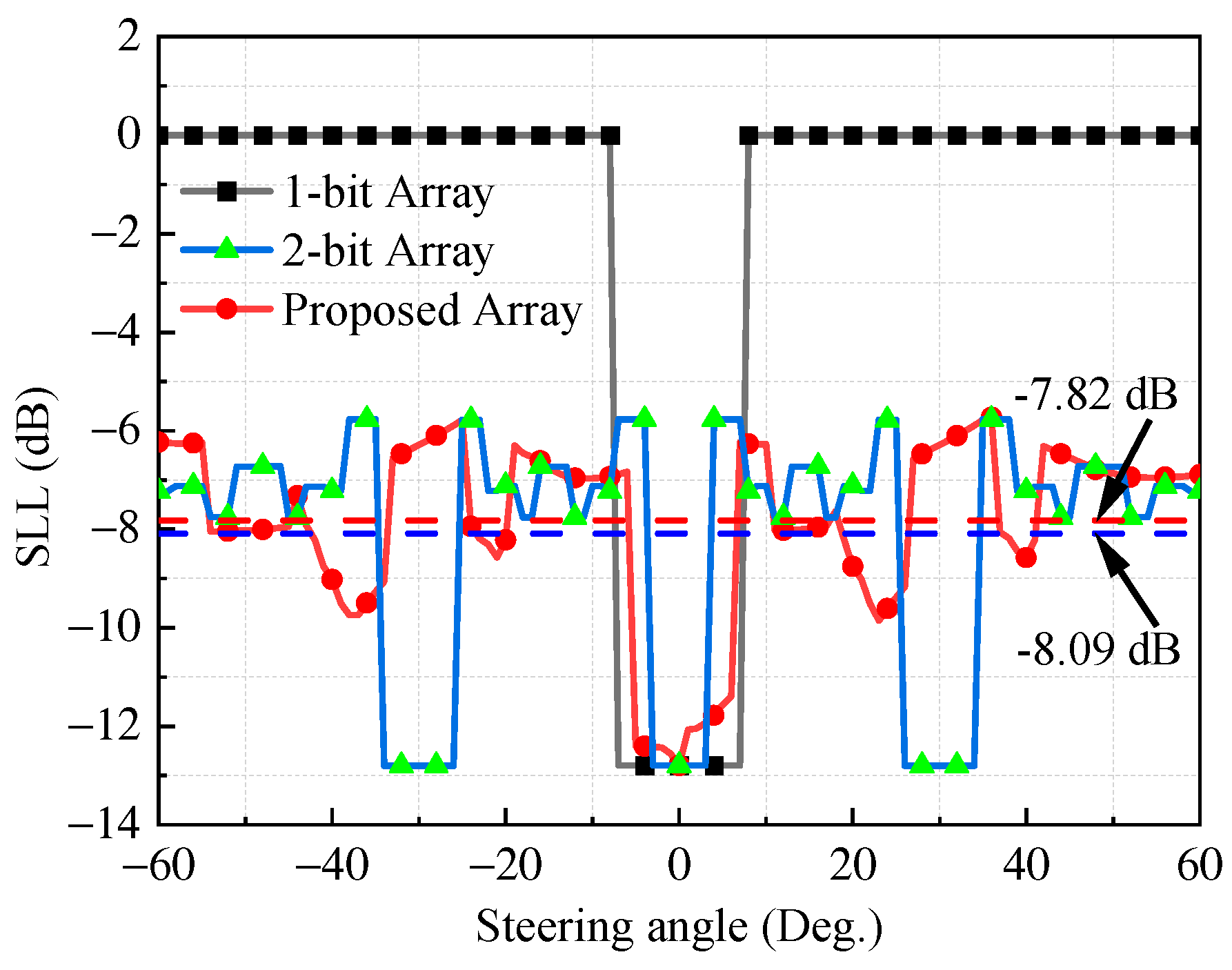
Figure 4 shows the simulated SLL versus beam-steering angle for the 1-bit, 2-bit, and proposed hybrid PSN-based phased arrays. The 1-bit array exhibited severe SLL degradation at large steering angles due to the periodic quantization errors of the phase shifters, which caused the sidelobes to rise to levels comparable to the main beam amplitude. In contrast, both the 2-bit and the proposed arrays maintained low sidelobes over the entire ± 60 ° scanning range. The average SLLs of the 2-bit and proposed arrays were −8.09 dB and −7.82 dB, respectively, which were substantially lower than that of the 1-bit array. The small difference of only 0.27 dB between the 2-bit and proposed arrays demonstrates that the proposed architecture achieves near−2-bit sidelobe suppression performance. Notably, the proposed design accomplishes this performance using only N + 2 control lines, whereas a conventional 2-bit array requires 2N control lines. This reduction greatly simplifies the biasing and routing networks.
Figure 4. Simulated result of the proposed array: SLL versus steering angle.
Overall, the proposed architecture maintains high η P A E as demonstrated in Figure 3) while effectively suppressing sidelobes, achieving an excellent trade-off among efficiency, control complexity, and implementation feasibility—making it well suited for large-scale, low-cost phased-array systems.

4. Element Design and Simulated Results

To realize low-cost and compact 1-bit phase control in phased arrays, this work adopted a reconfigurable antenna element that functions as a digitally controlled phase shifter. This antenna achieves a 180° phase shift through physical reconfiguration of the feed path. Specifically, by switching the excitation between two symmetric feed points, the surface current direction on the patch reverses, resulting in a spatial phase shift of 180°.
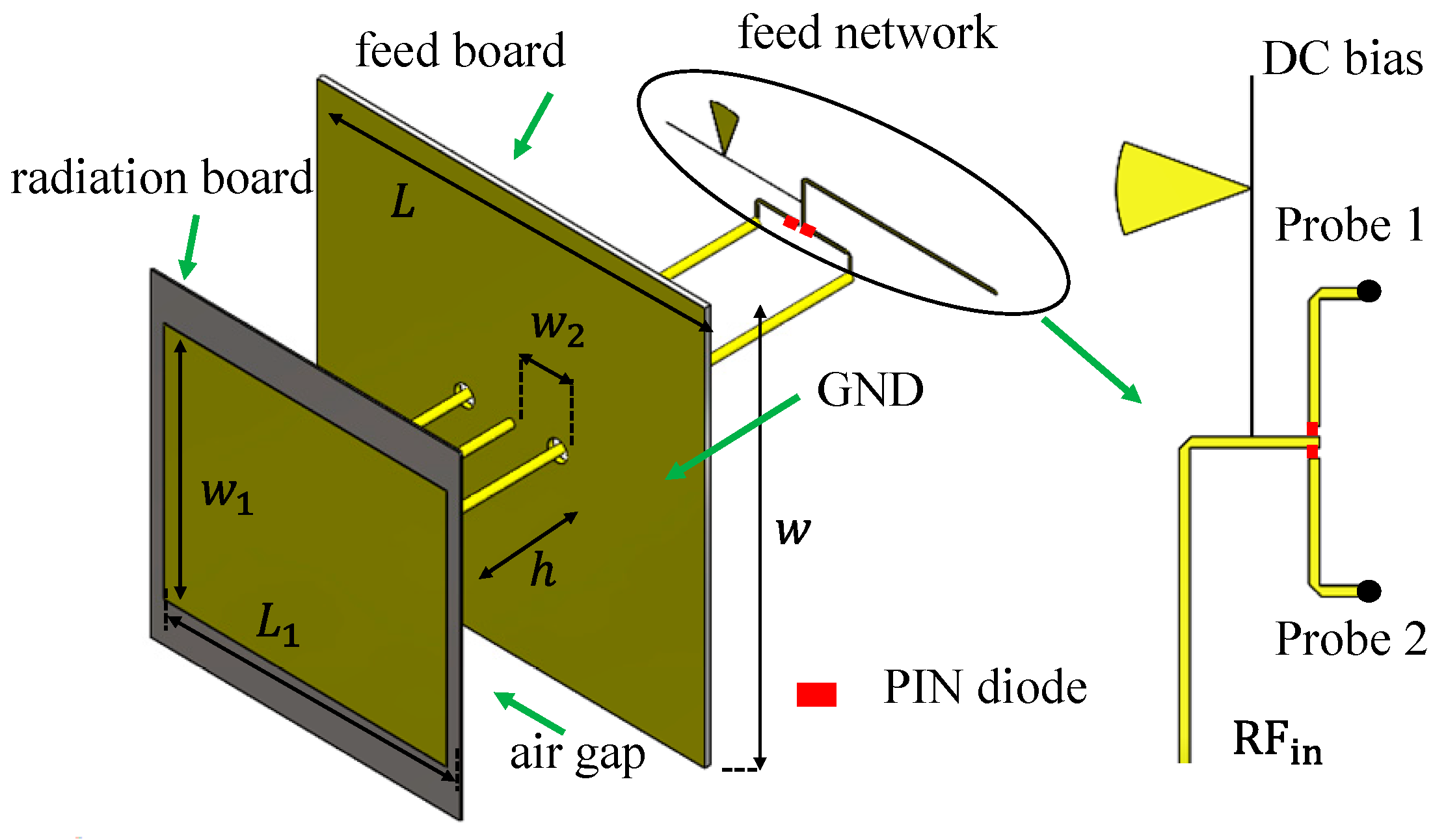
Figure 5 shows the detailed configuration of the proposed 1-bit antenna unit. The antenna comprises two printed circuit boards (PCBs): a radiation board and a feed board that incorporates a metallic ground plane. These two boards are separated by an air gap of height h which improves impedance matching and enhances radiation efficiency. The radiation board is fabricated from a 1 mm thick FR4 substrate and carries a rectangular patch that serves as the primary radiating element. The feed board is positioned beneath the radiation board and includes the ground plane together with a π-shaped feed network. This feed network consists of two symmetric feed probes that connect to the patch through vertical coaxial pins, two PIN diodes located at the junction of the feed lines, and a central grounding probe positioned between the feed probes. The grounding probe provides a direct current return path, ensuring electrical continuity and stabilizing the bias circuit. The feed network is connected to both the RF input port and the DC bias circuit. By applying different DC bias voltages, one of the PIN diodes is switched on while the other remains off, thereby selecting the active feed probe. When the excitation changes from Probe 1 to Probe 2, the surface current on the radiation patch reverses direction, resulting in an approximate 180° spatial phase shift. The detailed geometrical parameters of the antenna are summarized in Table 4.
Figure 5. Geometry of the proposed 1-bit unit antenna.
Table 4. Dimensions of the proposed 1-bit antenna unit (all dimensions are in millimeters).
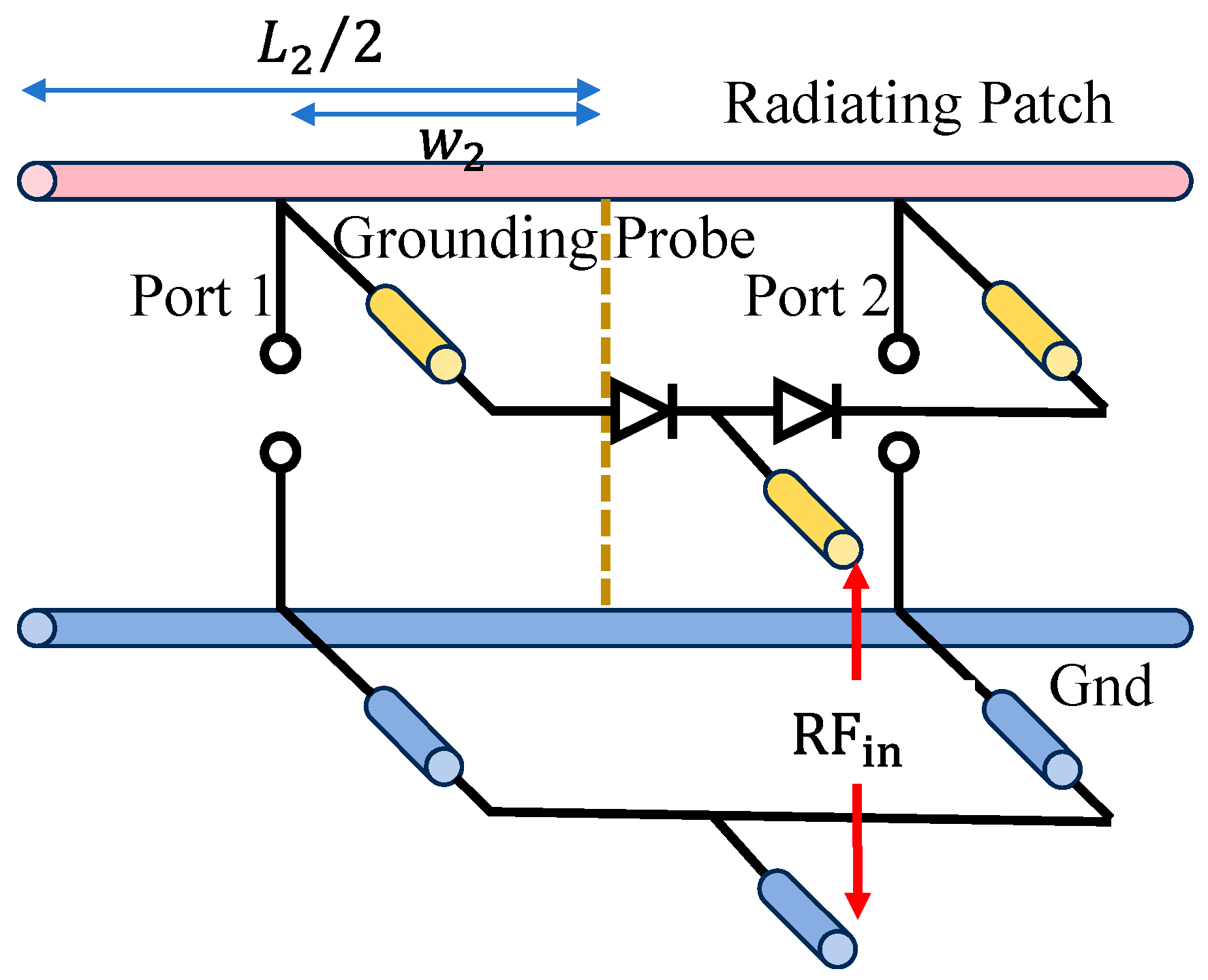
An equivalent schematic of the proposed 1-bit reconfigurable unit cell is presented in Figure 6 to illustrate the operating mechanism of the switching structure. The radiating patch is excited through two probes, denoted as Port 1 and Port 2, which are connected to the asymmetric microstrip feed network. A pair of PIN diodes is inserted between the two probe branches, forming a reconfigurable switching path that controls the dominant excitation port. When the diodes are biased in the ON state, the RF signal is primarily coupled to Port 1, whereas the OFF state shifts the excitation toward Port 2. The two biasing states result in opposite current distributions on the radiating patch, thereby generating the required 0° and 180° phase responses. A grounding probe is also included in the structure to provide a stable current-return path and maintain consistent switching behavior. The schematic highlights the essential RF paths and switching states of the unit cell and offers a simplified representation of the physical configuration shown in Figure 5.
Figure 6. Equivalent schematic of the proposed 1-bit unit cell.
In the simulation model, each PIN diode (BAR64-02V H6327) is represented by an equivalent circuit for the on and off states. When forward-biased, the diode is modeled as a series connection of a 1.8 Ω resistance and a 0.6 nH package inductance. When reverse-biased, it is modeled as a series combination of a 25 kΩ resistance, a 0.6 nH inductance, and a 0.35 pF junction capacitance. Considering that the forward conduction current of the PIN diode is approximately 20 mA, a 250 Ω current-limiting resistor is inserted in each DC bias line to prevent over-current damage and ensure stable biasing operation.
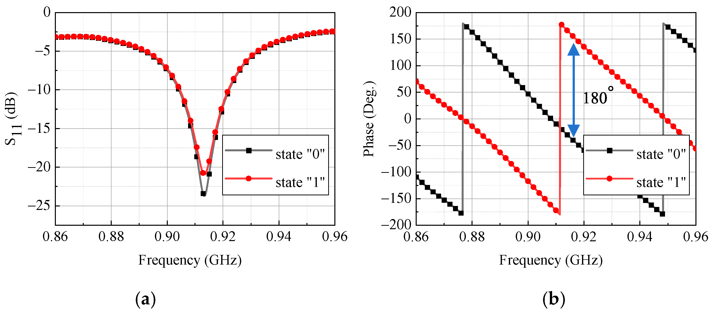
Figure 7a shows the simulated input reflection coefficients versus frequency for the two switching states. Due to the structural symmetry of the proposed antenna element, both states exhibited nearly identical impedance characteristics, with a common impedance bandwidth of 0.901–0.921 GHz, confirming stable impedance matching regardless of the switching state. Figure 7b illustrates that the phase difference between the two states remained approximately 180° within the impedance bandwidth.
Figure 7. Simulated results of the proposed 1-bit antenna unit at 0.915 GHz for states “0” and “1”: (a) reflection coefficient ( S 11 ); (b) corresponding phase response.
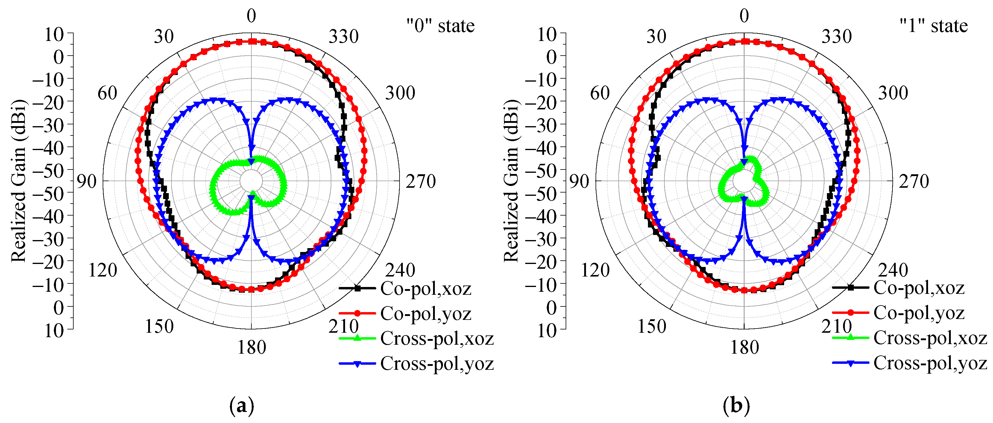
Figure 8a,b shows the simulated co-polarized far-field radiation patterns of the proposed 1-bit antenna unit under the two operating states. The co-polarization gains of both states were nearly identical, with a maximum gain of 6.25 dBi and a half-power beamwidth of approximately ± 38 ° . Moreover, the phase transition between the two states introduced negligible amplitude fluctuation, indicating low insertion-loss fluctuation and stable radiation behavior during state switching.
Figure 8. Simulated radiation performance of the proposed 1-bit antenna unit at 0.915 GHz under (a) state “0” and (b) state “1”.

5. Experimental Validation

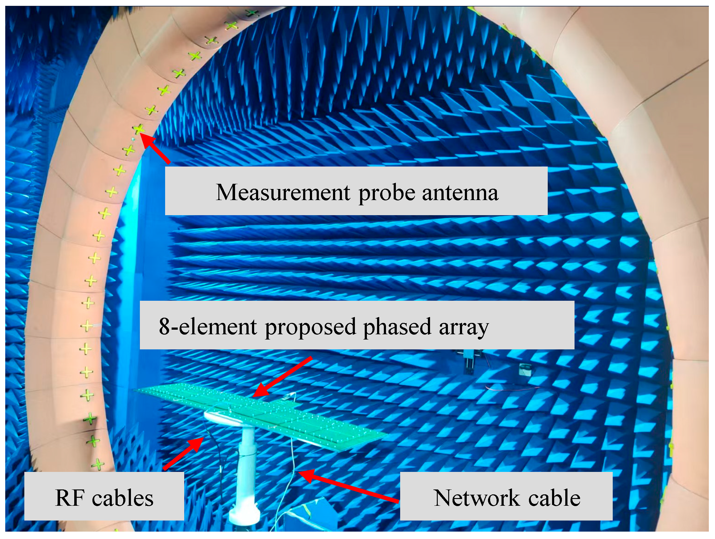
Based on the reconfigurable antenna unit described above, a proposed 8-element phased-array prototype integrating the proposed low-complexity hybrid PSN was fabricated and experimentally characterized. A 1-to-8 power divider was employed to provide equal-amplitude and in-phase microwave signals to each antenna element, with an inter-element spacing of half a wavelength. The far-field measurement was conducted inside a microwave anechoic chamber using the setup shown in Figure 9. The measurement configuration included the 8-element phased array under test, a measurement probe antenna, RF cables for signal transmission, and a network cable for control communication. Each antenna element’s PIN diode was biased between ±5 V to realize the 0° and 180° digital phase states, forming the digital control part. The proposed hybrid PSN adopted a shared control structure consisting of one global analog voltage line and one digital switching line, resulting in a total of only ten control lines for the entire array.
Figure 9. Experimental setup for measuring the radiation performance of the proposed 8-element phased array in a microwave anechoic chamber.
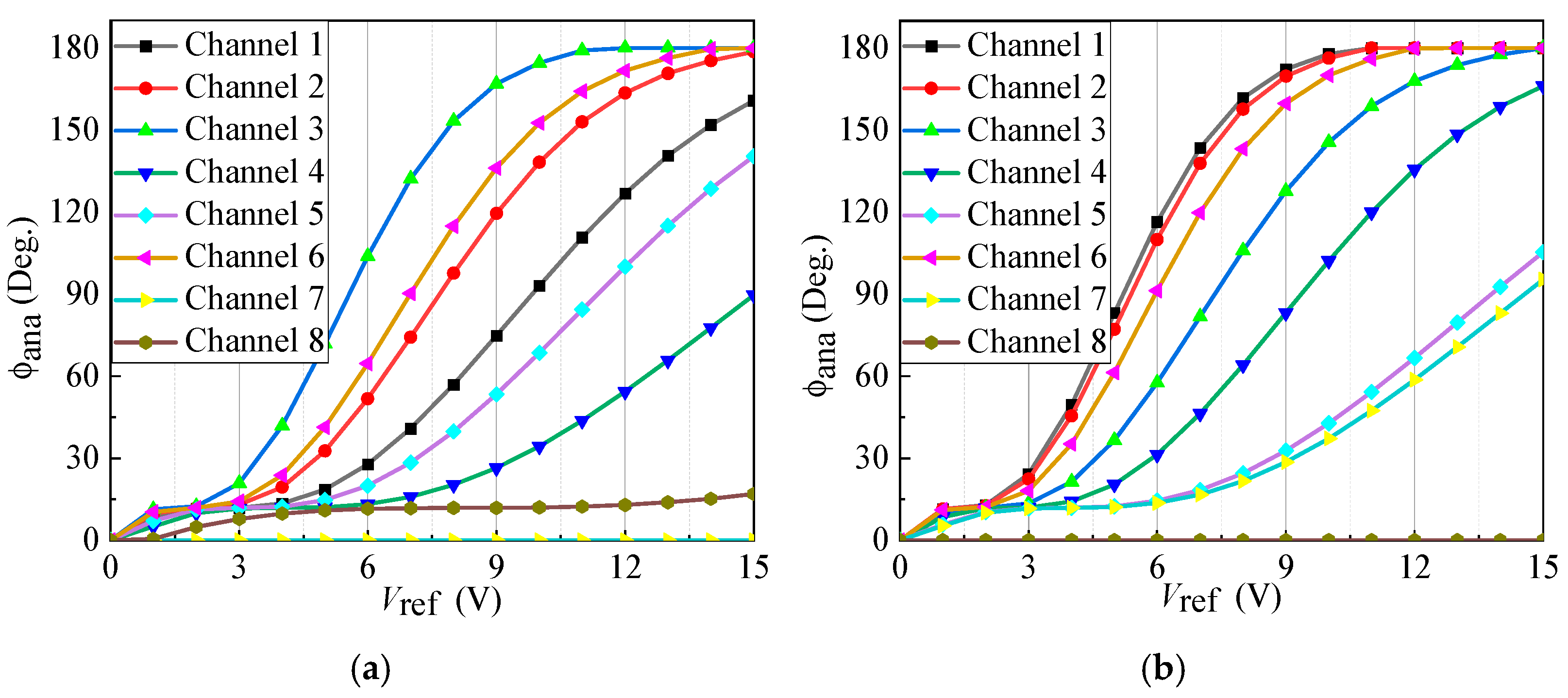
Due to the non-isotropic radiation patterns of the antenna elements, direction-dependent variations arise in the array response. To mitigate this effect and enhance beamforming accuracy, the design of the division ratio vectors in the hybrid PSN was informed by the measured element patterns. Table 5 summarizes the optimized two division ratio vectors. Figure 10 displays the analog phase shift characteristics of all eight channels corresponding to the two optimized division ratio vectors. As a result, by continuously tuning a single V r e f , distinct phase shifts can be simultaneously induced across different channels.
Table 5. The division ratio vectors under g = 1 , 2 .
Figure 10. Voltage-controlled phase shifter Ø a n a versus V r e f for all channels under (a) g = 1 and (b) g = 2 .
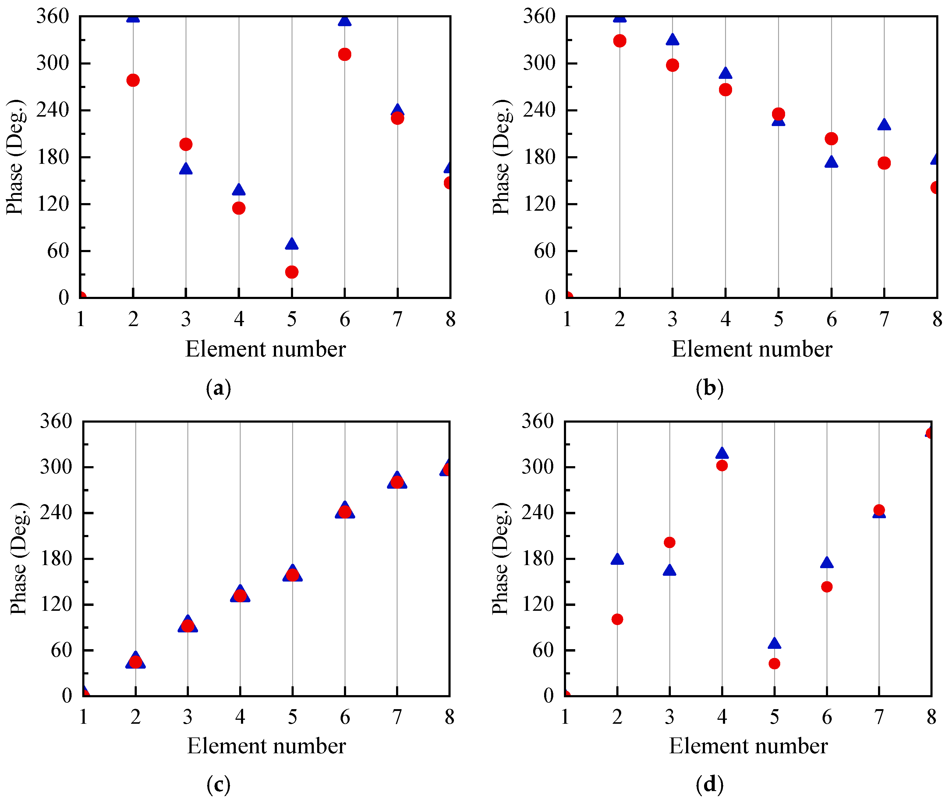
To further assess the beamforming capability of the proposed scheme, the actual excitation phases Ø r e a , n applied to each antenna element were measured and compared with the ideal excitation phases Ø r e a , n for four steering angles: 27 ° , 10 ° , 14 ° , and 32 ° . As shown in Figure 11, the measured phases closely matched the ideal distributions across all cases, demonstrating that the proposed system can accurately synthesize the desired phase profiles for various beam directions. This performance was achieved using only a single additional shared control voltage V r e f which significantly reduces the control complexity compared to conventional per-channel control methods.
Figure 11. Comparison between the ideal excitation phase Ø i d , n (red circles) and the actual excitation phase Ø r e a , n (blue triangles) under four beam steering angles: (a) −27°, (b) −10°, (c) 14°, and (d) 32°.
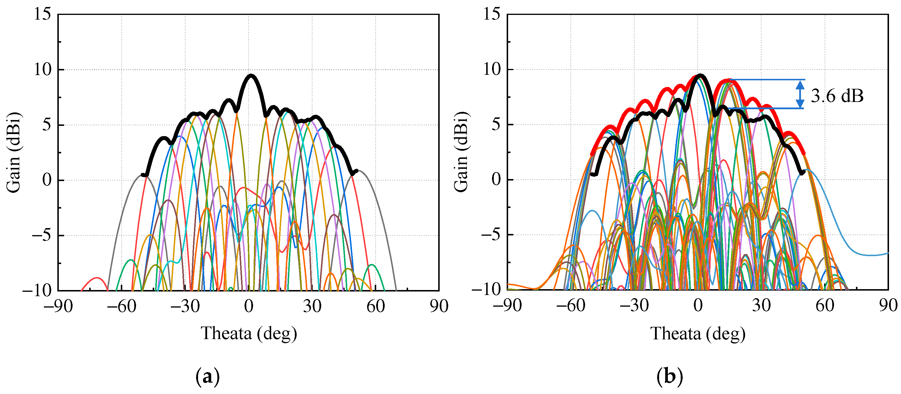
Figure 12 presents the measured radiation patterns of the proposed hybrid analog–digital PSN. The multiple colored thin curves correspond to the radiation patterns measured under different steering angles and control states. The bold black curve represents the scanning envelope of the conventional 1-bit phased array, while the bold red curve shows the enhanced scanning envelope achieved by the proposed architecture. By employing only two additional shared control paths, the proposed array achieves a peak main-lobe gain improvement of 3.6 dB and a maximum SLL reduction to −4 dB, compared with the conventional 1-bit phased array, while maintaining stable beam performance within the ±50° steering range. These results clearly demonstrate that the proposed design significantly improves beamforming performance and radiation efficiency over the 1-bit array, while retaining remarkable hardware simplicity.
Figure 12. Measured 2-D far-field radiation patterns of the 8-element phased array: (a) using a 1-bit phase control scheme; (b) using a hybrid PSN with shared-control voltage.
Therefore, the hybrid PSN provides a practical and scalable solution that effectively balances array performance, implementation cost, and control complexity, making it highly suitable for large-scale, low-cost phased-array applications.

6. Conclusions

This paper presented a low-complexity hybrid PSN based on a shared-control voltage architecture for high-gain phased-array applications operating at 0.915 GHz. Each channel integrates a 1-bit reconfigurable antenna and a voltage-controlled phase shifter, enabling continuous 0–360° phase tuning with an insertion loss below −1.2 dB and an amplitude fluctuation within ±0.2 dB. Compared with switched-type or reflective-type phase shifters, the proposed design exhibited lower insertion loss and minimal amplitude fluctuation. By employing reconfigurable passive resistor dividers, a single analog voltage source can simultaneously bias all channels, eliminating the need for per-channel voltage sources and substantially reducing system complexity. Compared with a conventional 1-bit PSN, the proposed architecture achieved up to 3.6 dB improvement in main-lobe gain while requiring only two additional control lines, thus demonstrating an excellent balance between performance and implementation simplicity.
Although experimentally verified at 0.915 GHz, the shared-control concept is frequency-independent and can be readily applied to high-frequency phased-array systems. Furthermore, the proposed hybrid PSN with shared-control architecture is not limited to linear arrays; it can be extended to planar or conformal arrays by employing orthogonal shared-control voltages or subarray-based voltage-distribution networks, thereby enabling two-dimensional beam steering while maintaining hardware simplicity. These characteristics make the proposed PSN a scalable, energy-efficient, and cost-effective solution for next-generation phased-array systems.

Author Contributions

Conceptualization, H.S., X.M. and D.Z.; methodology, X.M. and R.H.; software, H.S. and X.M.; validation, X.M. and R.H.; formal analysis, H.S. and X.M.; investigation, R.H.; resources, D.Z.; data curation, X.M.; writing—original draft preparation, R.H.; writing—review and editing, D.Z.; visualization, R.H.; supervision, D.Z.; project administration, D.Z.; funding acquisition, D.Z. All authors have read and agreed to the published version of the manuscript.

Funding

This research was funded by the Science and Technology on Space Physics Laboratory, no. H04W241159.

Data Availability Statement

The original contributions presented in this study are included in the article. Further inquiries can be directed to the corresponding author.

Conflicts of Interest

The authors declare no conflicts of interest.

References

  1. Naqvi, A.H.; Lim, S. Review of Recent Phased Arrays for Millimeter-Wave Wireless Communication. Sensors 2018, 18, 3194. [Google Scholar] [CrossRef]
  2. Fujishima, M. Advancements in Terahertz Communication: Harnessing the 300 GHz Band for High-Efficiency, High-Capacity Wireless Networks. IEICE Trans. Electron. 2024, E107C, 366–375. [Google Scholar] [CrossRef]
  3. Ushio, T.; Wada, Y.; Yoshida, S. Recent Advances in Phased Array Weather Radar. IEICE Trans. Electron. 2024, E107C, 274–278. [Google Scholar] [CrossRef]
  4. Fujimoto, T. Japanese Institutionalization and Global Standardization of Wireless Power Transmission, and Recently R&D Trend in Japan. IEICE Trans. Electron. 2024, E107C, 299–306. [Google Scholar] [CrossRef]
  5. Jiang, W.; Guo, Y.C.; Liu, T.H.; Shen, W.F.; Cao, W. Comparison of random phasing methods for reducing beam pointing errors in phased array. IEEE Trans. Antennas Propag. 2003, 51, 782–787. [Google Scholar] [CrossRef]
  6. Kebe, M.; Yagoub, M.C.E.; Amaya, R.E. A Survey of Phase Shifters for Microwave Phased Array Systems. Int. J. Circuit Theory Appl. 2025, 53, 3719–3739. [Google Scholar] [CrossRef]
  7. Pang, J.; Wu, R.; Wang, Y.; Dome, M.; Kato, H.; Huang, H.; Narayanan, A.T.; Liu, H.; Liu, B.; Nakamura, T.; et al. A 28-GHz CMOS Phased-Array Transceiver Based on LO Phase-Shifting Architecture with Gain Invariant Phase Tuning for 5G New Radio. IEEE J. Solid-State Circuits 2019, 54, 1228–1242. [Google Scholar] [CrossRef]
  8. Avitabile, G.; Man, K.L.; Talarico, C. DDS-PLL Architecture for Adaptive Beam Steering. In Proceedings of the 2024 21st International SoC Design Conference (ISOCC), Sapporo, Japan, 19–22 August 2024; pp. 205–206. [Google Scholar] [CrossRef]
  9. Florio, A.; Coviello, G.; Talarico, C.; Avitabile, G. Adaptive DDS-PLL Beamsteering Architecture based on Real-Time Angle-of-Arrival Estimation. In Proceedings of the 2024 IEEE 67th International Midwest Symposium on Circuits and Systems (MWSCAS), Springfield, MA, USA, 11–14 August 2024; pp. 628–631. [Google Scholar] [CrossRef]
  10. Florio, A.; Coviello, G.; Talarico, C.; Avitabile, G. Adaptive Beamsteering Architecture Based on AoA Estimation with Phase Shift on LO-Path for 5G NR. In Proceedings of the 2024 9th International Conference on Smart and Sustainable Technologies (SpliTech), Bol and Split, Croatia, 25–28 June 2024; pp. 1–5. [Google Scholar] [CrossRef]
  11. Li, S.; Zhang, Z.; Rebeiz, G.M. An Eight-Element 136–147 GHz Wafer-Scale Phased-Array Transmitter with 32 dBm Peak EIRP and >16 Gbps 16QAM and 64QAM Operation. IEEE J. Solid-State Circuits 2022, 7, 1635–1648. [Google Scholar] [CrossRef]
  12. Li, S.; Zhang, Z.; Rupakula, B.; Rebeiz, G.M. An Eight-Element 140-GHz Wafer-Scale IF Beamforming Phased-Array Receiver with 64-QAM Operation in CMOS RFSOI. IEEE J. Solid-State Circuits 2021, 57, 385–399. [Google Scholar] [CrossRef]
  13. Verho, S.; Chung, J.-Y. Design of a Compact and Minimalistic Intermediate Phase Shifting Feed Network for Ka-Band Electrical Beam Steering. Sensors 2024, 24, 1235. [Google Scholar] [CrossRef]
  14. D’Amato, G.; Avitabile, G.; Coviello, G.; Talarico, C. DDS-PLL Phase Shifter Architectures for Phased Arrays: Theory and Techniques. IEEE Access 2019, 7, 19461–19470. [Google Scholar] [CrossRef]
  15. Kibaroglu, K.; Sayginer, M.; Rebeiz, G.M. A Low-Cost Scalable 32-Element 28-GHz Phased Array Transceiver for 5G Communication Links Based on a 2 × 2 Beamformer Flip-Chip Unit Cell. IEEE J. Solid-State Circuits 2018, 53, 1260–1274. [Google Scholar] [CrossRef]
  16. Sadhu, B.; Tousi, Y.; Hallin, J.; Sahl, S.; Reynolds, S.K.; Renström, Ö.; Sjögren, K.; Haapalahti, O.; Mazor, N.; Bokinge, B.; et al. A 28-GHz 32-Element TRX Phased-Array IC with Concurrent Dual-Polarized Operation and Orthogonal Phase and Gain Control for 5G Communications. IEEE J. Solid-State Circuits 2017, 52, 3373–3391. [Google Scholar] [CrossRef]
  17. Liang, Q.; Zhang, Y.; Wang, K.; Yan, Y.; Liang, X. A novel 6.5–13.5GHz 6-bit digital phase shifter with ultra low RMS phase error in 0.25-µm GaAs p-HEMT technology. IEICE Electron. Express 2024, 21, 20240143. [Google Scholar] [CrossRef]
  18. Zhao, H.T.; Entesari, K.; Hoyos, S. Multi-Channel Analog Beamforming Transceiver for mmWave Communications. IEEE. Trans. Mob. Comput. 2025, 24, 6106–6118. [Google Scholar] [CrossRef]
  19. Abbasi, M.; Lee, W. A Low-Loss Passive D-Band Phase Shifter for Calibration-Free, Precise Phase Control. IEEE J. Solid-State Circuit 2024, 59, 1371–1380. [Google Scholar] [CrossRef]
  20. Lee, J.; Jeong, J.; Kim, D.; Kim, S. A 19.5 GHz 5-bit digitally programmable phase shifter for active antenna arrays. Electronics 2023, 12, 2862. [Google Scholar] [CrossRef]
  21. Seo, S.; Lee, J.; Lee, Y.; Shin, H. A 28 GHz GaN 6-Bit Phase Shifter MMIC with Continuous Tuning Calibration Technique. Sensors 2024, 24, 1087. [Google Scholar] [CrossRef]
  22. Lin, C.S.; Chang, S.F.; Chang, C.C.; Shu, Y.H. Design of a Reflection-Type Phase Shifter with Wide Relative Phase Shift and Constant Insertion Loss. IEEE Trans. Microw. Theory Tech. 2007, 55, 1862–1868. [Google Scholar] [CrossRef]
  23. Wu, J.C.; Chang, C.C.; Chang, S.F.; Chin, T.Y. A 24-GHz full-360° CMOS reflection-type phase shifter MMIC with low loss-variation. In Proceedings of the IEEE Radio Frequency Integrated Circuits Symposium (RFIC), Atlanta, GA, USA, 15–17 June 2008; pp. 327–330. [Google Scholar]
  24. Fakharzadeh, M.; Mousavi, P.; Safavi-Naeini, S.; Jamali, S.H. The effects of imbalanced phase shifters loss on phased array gain. IEEE Antennas Wirel. Propag. Lett. 2008, 7, 192–196. [Google Scholar] [CrossRef]
  25. Garg, R.; Natarajan, A. A 28-GHz Low-Power Phased-Array Receiver Front-End with 360° RTPS Phase Shift Range. IEEE Trans. Microw. Theory Tech. 2017, 65, 4703–4714. [Google Scholar] [CrossRef]
  26. Li, T.-W.; Wang, H. A Millimeter-Wave Fully Integrated Passive Reflection-Type Phase Shifter with Transformer-Based Multi-Resonance Loads for 360° Phase Shifting. IEEE Trans. Circuits Syst. I Regul. Pap. 2017, 65, 1406–1419. [Google Scholar] [CrossRef]
  27. Ye, Y.F.; Wang, Y.T.; Feng, J.H.; Wu, L.S.; Qiu, L.F.; Mao, J.F. A Compact Ka-Band Hybrid Analog/Digital Phase Shifter with GaAs Technology. IEEE Trans. Circuits Syst. II-Express Briefs 2024, 71, 1834–1838. [Google Scholar] [CrossRef]
  28. Zheng, S.; Wang, Y.; Deng, Z.; Jiang, C.; Xu, H. A 22.5~28.5-GHz Low-Amplitude-Variation Low-Phase-Error Hybrid Phase Shifter Using Flatness Enhancement Techniques for 5G NR in 40nm CMOS. IEEE Trans. Circuits Syst. II Express Briefs 2025, 72, 813–817. [Google Scholar] [CrossRef]
  29. Xia, J.J.; Farouk, M.; Boumaiza, S. Digitally-Assisted 27–33 GHz Reflection-Type Phase Shifter with Enhanced Accuracy and Low IL-Variation. In Proceedings of the IEEE Radio Frequency Integrated Circuits Symposium (RFIC), Boston, MA, USA, 2–4 June 2019; pp. 63–66. [Google Scholar]
  30. Al-Khalidi, A.H.; Ahmed, M.M.; Abdullah, S.A. Uniform Linear Antenna array Beamsteering Based on Progressive Phase. Electronics 2023, 12, 780. [Google Scholar] [CrossRef]
  31. Sánchez-Sevilleja, S.; García-Rodríguez, M.; Masa-Campos, J.L.; Cuerda-Muñoz, J.M. Antenna Model with Pattern Optimization Based on Genetic Algorithm for Satellite-Based SAR Mission. Sensors 2025, 25, 4835. [Google Scholar] [CrossRef]
Disclaimer/Publisher’s Note: The statements, opinions and data contained in all publications are solely those of the individual author(s) and contributor(s) and not of MDPI and/or the editor(s). MDPI and/or the editor(s) disclaim responsibility for any injury to people or property resulting from any ideas, methods, instructions or products referred to in the content.

Article Metrics

Citations

Article Access Statistics

Multiple requests from the same IP address are counted as one view.