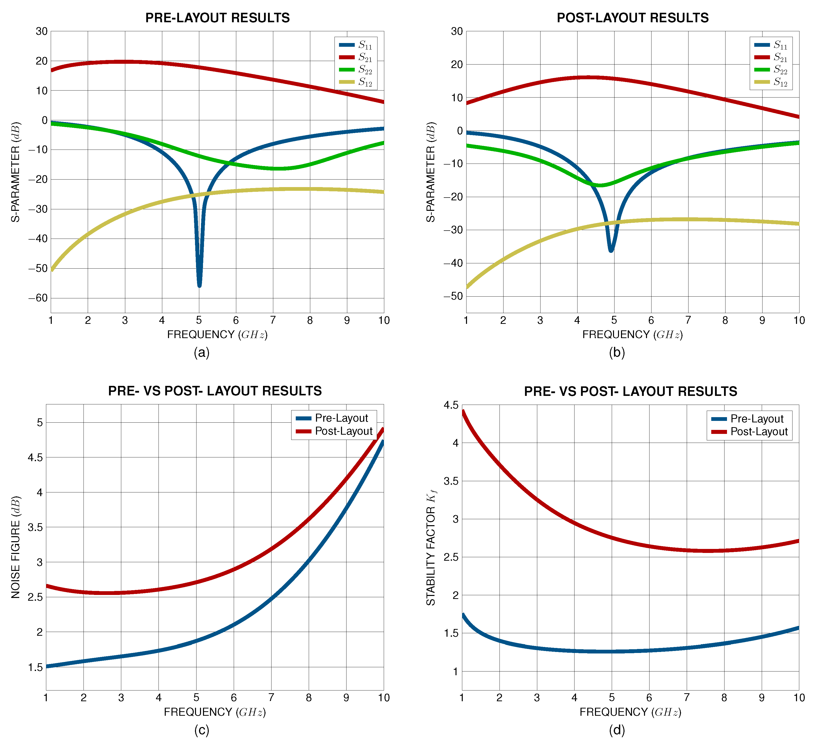
Having defined the essential cost functions of each circuit, detailed design methodologies are synthesized. Each design methodology developed in this work is based on the corresponding cost functions that adequately describe the circuits undergoing testing. In the LNA scheme, scattering and impedance parameters are utilized for the input impedance matching of the LNA, while the minimum noise figure parameter is employed for the transistor sizing. In the VCO scheme, the impedance and admittance parameters are employed for the LC-tank and optimal inductor characterizations, respectively. For the VCO’s transistor sizing, the boundary condition for oscillation cost function is used where the Z-Parameters are exploited.
3.1. LNA Design Methodology
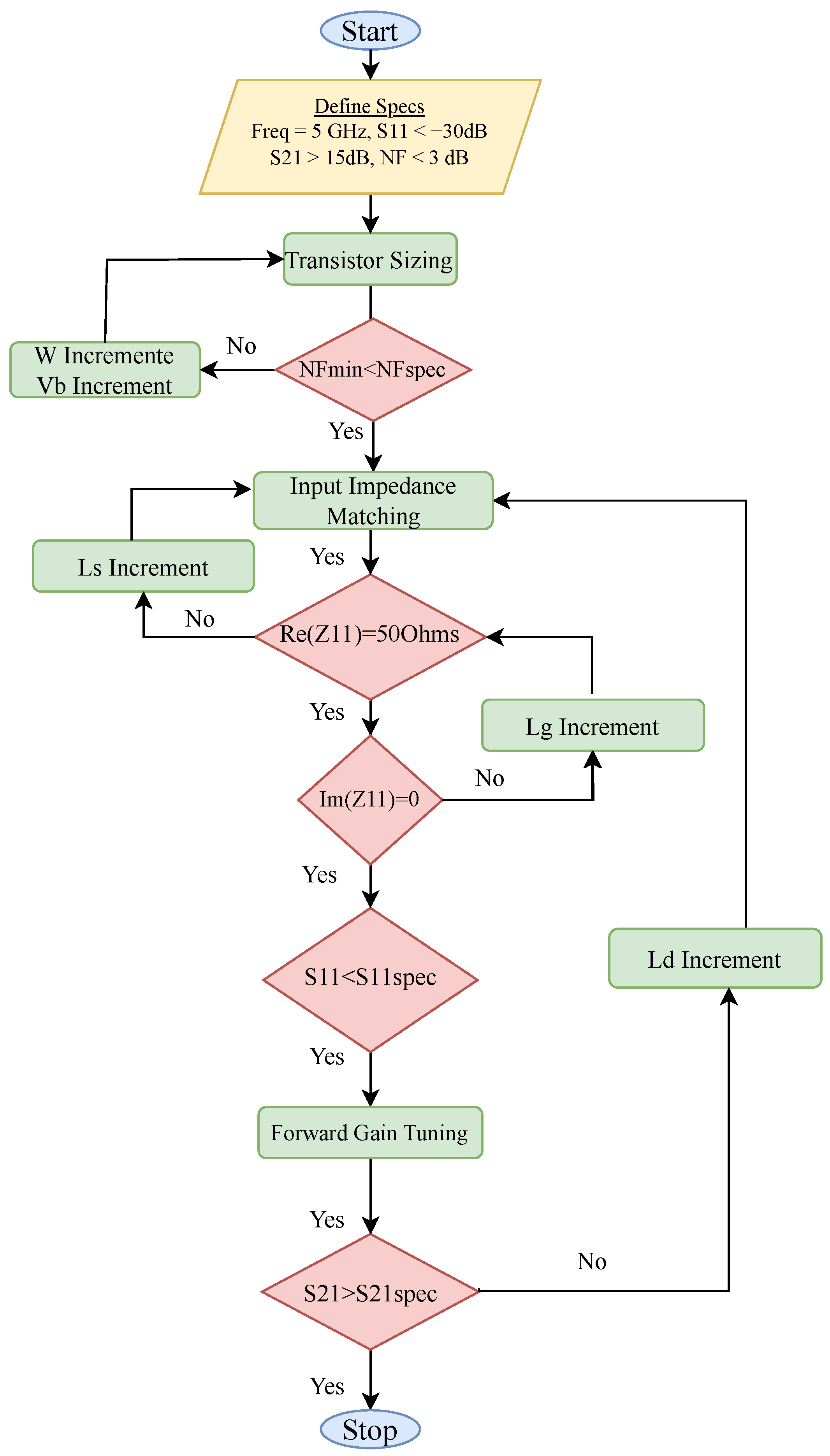
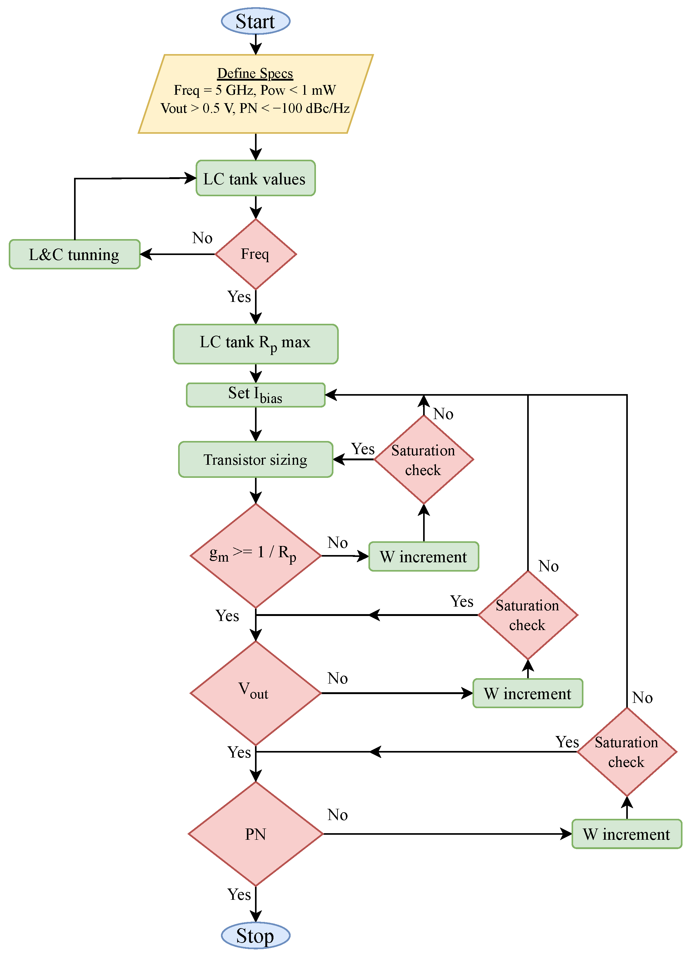
The proposed methodology for designing an LNA is outlined with a flowchart and a pseudo-code, as depicted in
Figure 13 and Algorithm 1, respectively, offering a structured framework for achieving the desired performance specifications. The design process begins with defining key specifications and the transistor PDK limits. The specifications include the operating frequency
, the target input reflection coefficient
, the desired forward gain
, and the noise figure
of the LNA being tested.
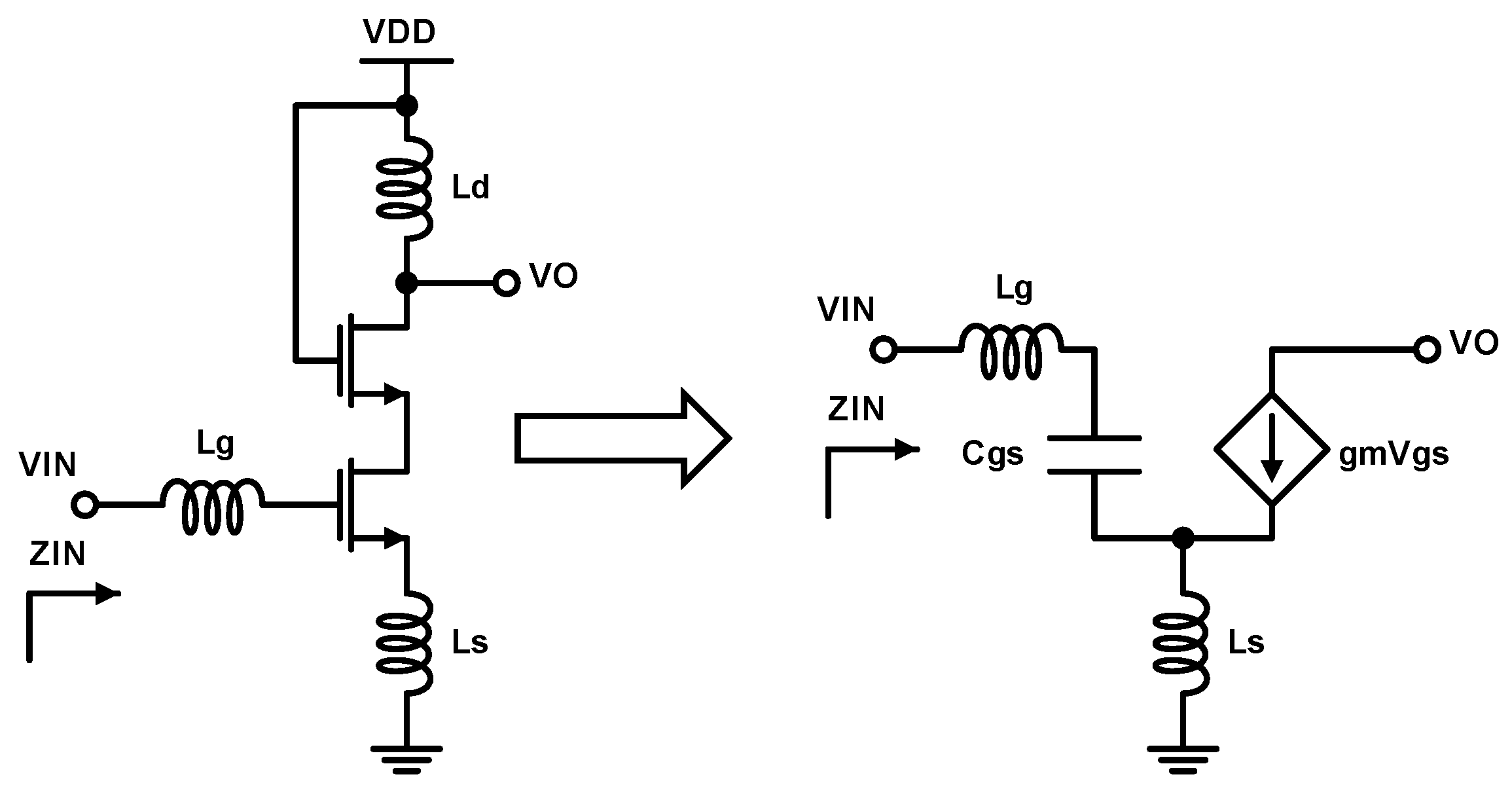
The first phase involves transistor sizing, which directly impacts the noise figure. The transistor’s width and the bias voltage are adjusted to ensure that the minimum noise figure
value does not exceed the target noise figure
value. As evident from
Figure 2, the
parameter exhibits a minimum value within a specific range of transistor widths and bias points, which scale with power consumption. As the transistor width increases, transconductance
and gate-to-source capacitance
increase. Therefore, based on (6) and (7), careful selection of the transistor width is necessary to achieve the minimum
value while also enabling input impedance matching to
. If the condition
is not met, adjustments are systematically applied to the transistor’s width and bias point until the noise specifications are satisfied. If not, the transistor sizing at the absolute minimum of the
parameter should be returned, thus breaking the transistor sizing procedure loop.
| Algorithm 1 LNA Design Methodology |
- 1:
Define Min and Max values according to PDK limits: - 2:
Transistor min Channel Width → - 3:
Transistor min Channel Length → - 4:
- 5:
Define LNA Specifications and Parameters: - 6:
Operating Frequency → - 7:
Voltage Supply → - 8:
Bias Voltage → - 9:
Gate Inductor → - 10:
Source Degeneration Inductor → - 11:
Input Impedance Matching → - 12:
Forward Gain → - 13:
Noise Figure → - 14:
- 15:
LNA Cost Functions: - 16:
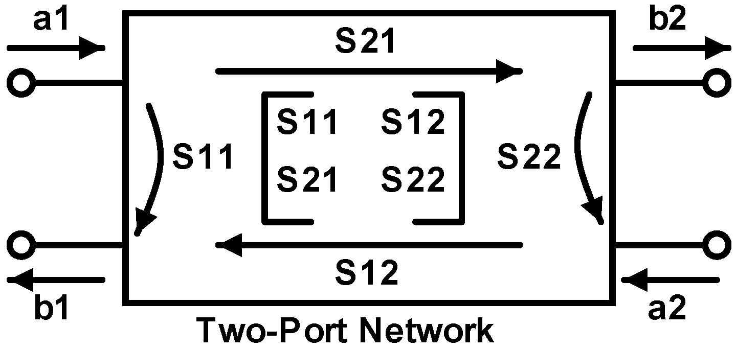
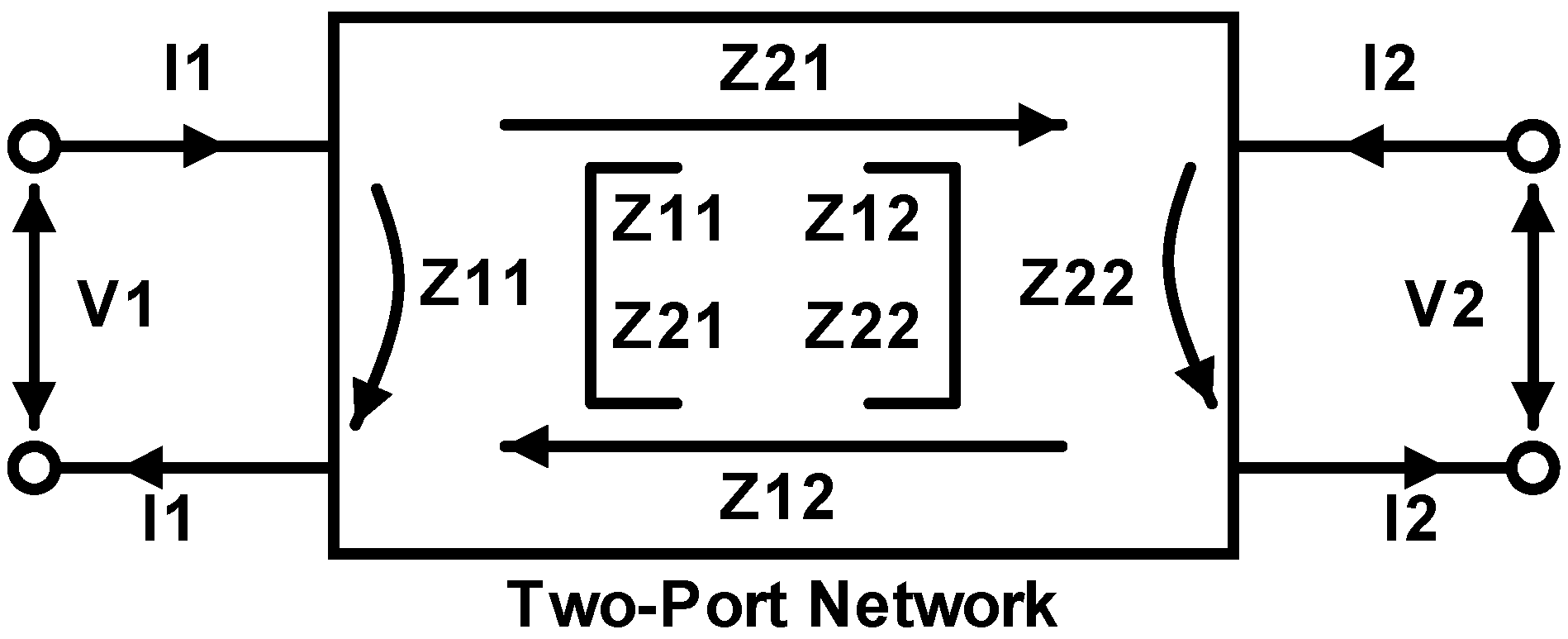
: Returns the minimum Noise Figure for a given transistor width W, monitored at the frequency while applying a biasing. - 17:
: Returns the real part of the input impedance at the specified frequency , sweeping the parameter X. - 18:
: Returns the imaginary part of the input impedance at the specified frequency , sweeping the parameter X. - 19:
- 20:
Main Optimization Algorithm: - 21:
while (TRUE) { - 22:
// Transistor Sizing - 23:
for loop { - 24:
for loop { - 25:
- 26:
if () return W and }} - 27:
// Input Impedance Matching - 28:
while { - 29:
for loop { - 30:
- 31:
if return break}} - 32:
while { - 33:
for loop { - 34:
- 35:
if return break}} - 36:
if { - 37:
go to Input Impedance Matching } - 38:
// Forward Gain Tuning - 39:
else if { - 40:
for loop { - 41:
while { - 42:
if return break }}} - 43:
end
|
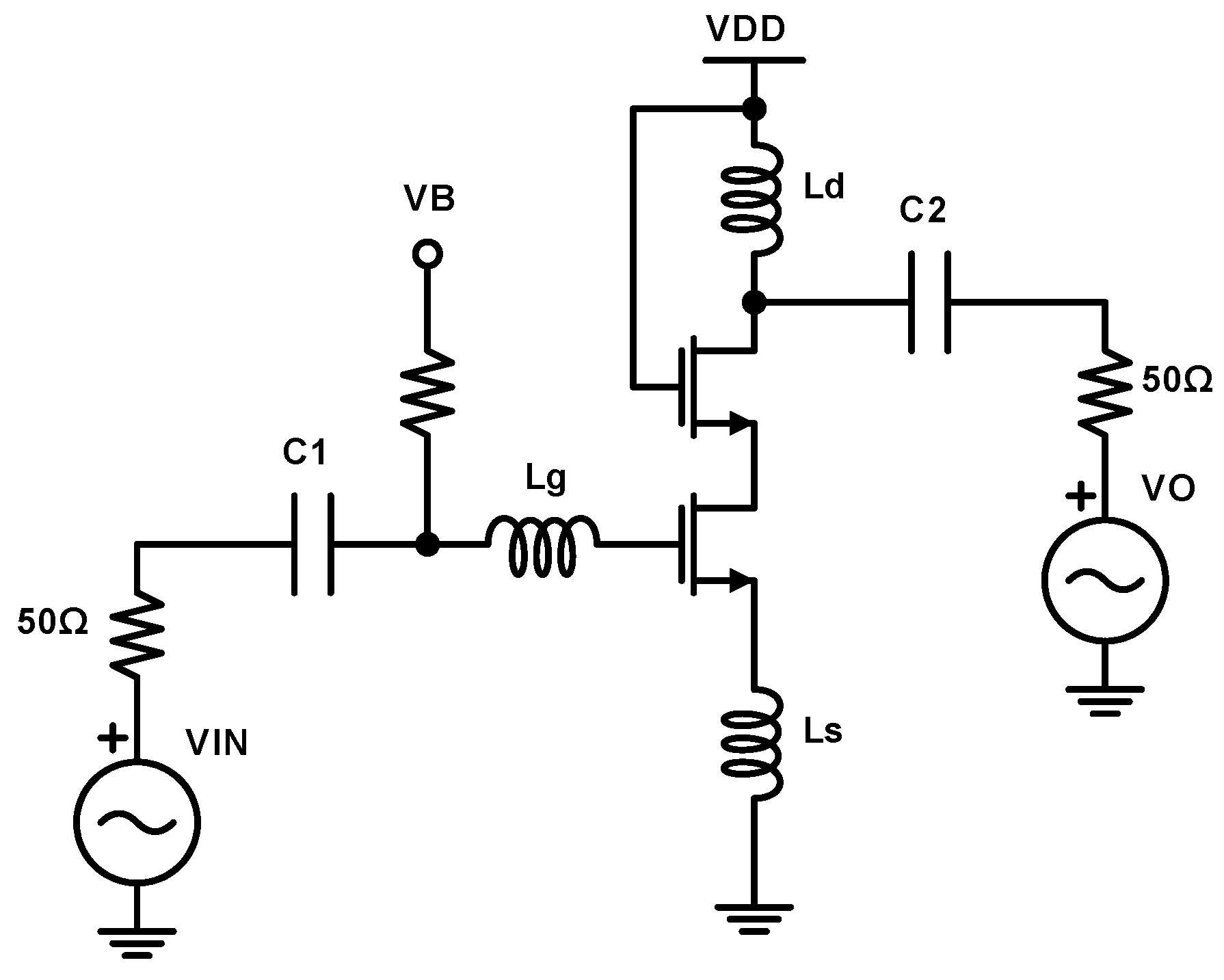
Once the noise performance is optimized, attention shifts to achieving proper input impedance matching. This requires ensuring that the real part of the input impedance equals the antenna impedance of , to enable maximum power transfer and minimal reflection. If , the source degeneration inductance is incrementally adjusted until this condition is met. Simultaneously, the imaginary component of the input impedance should satisfy the condition by tuning the gate inductance . Together, these adjustments ensure that the amplifier’s input is optimally matched to the source impedance. The iterative tuning process continues until the input reflection coefficient is less than or equal to the target . This ensures that the amplifier achieves high efficiency and minimal signal loss at the interface with no wave reflections back to the antenna.
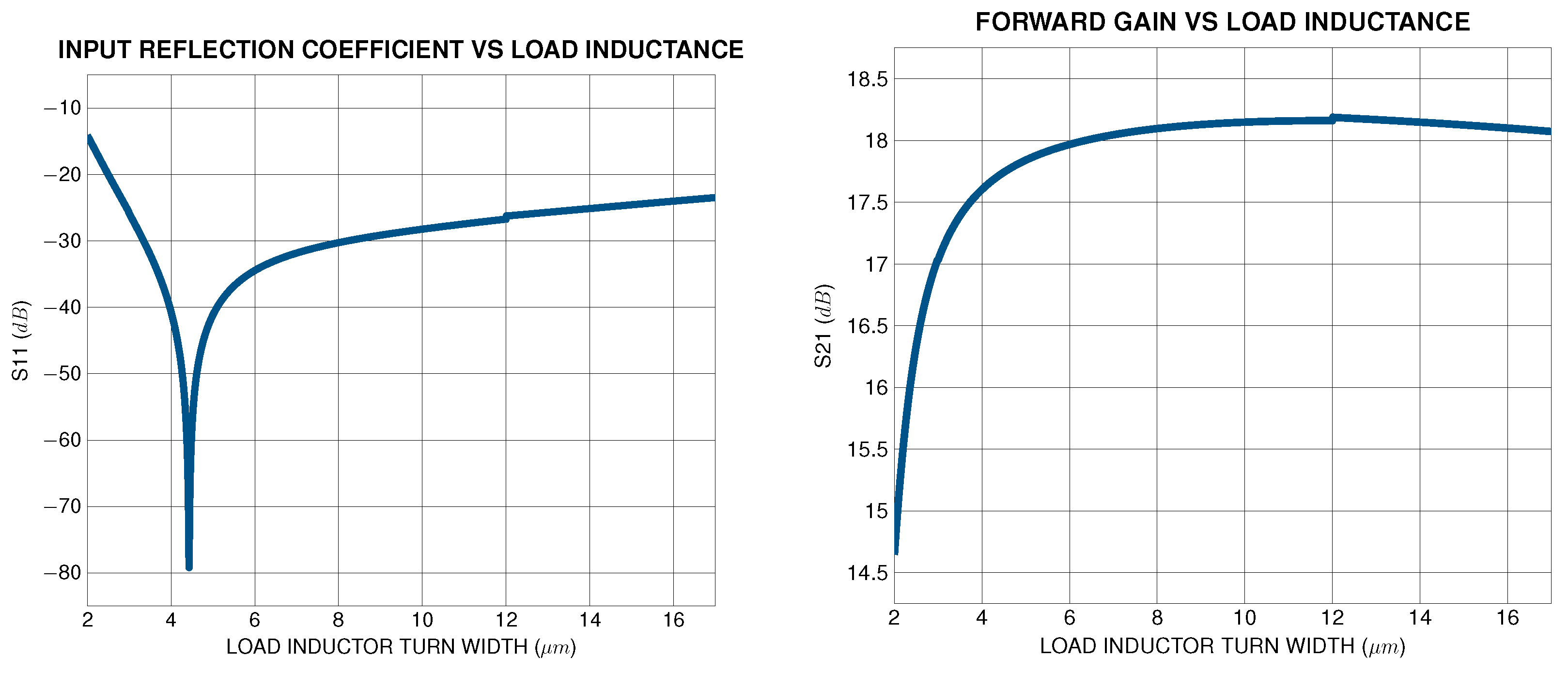
Following the impedance matching stage, forward gain optimization is performed in order to tune the amplifier’s gain to the desired value, dictated by the
specification. If the achieved gain is less than the specified
, the load inductance
is incrementally increased, affecting the amplifier’s gain. However, any adjustments to
inherently alter the input impedance matching, as illustrated in
Figure 14, necessitating a repetition of the input impedance matching process so as to maintain the input matching criteria. This iterative loop of gain enhancement and impedance re-tuning ensures that the forward gain meets
without compromising other performance metrics of the LNA. The methodology terminates once all design specifications are fulfilled, resulting in a robust and efficient LNA design.
3.2. VCO Design Methodology
The proposed VCO methodology is outlined again using a flowchart and a pseudo-code representation of the developed methodology, as depicted in
Figure 15 and Algorithm 2, respectively. The design process begins with defining key specifications and the PDK limits of the respective models, used in the design. The specifications include the oscillation frequency
, the target output voltage swing
, and the phase noise performance
, while maintaining the power consumption of the VCO
mW.
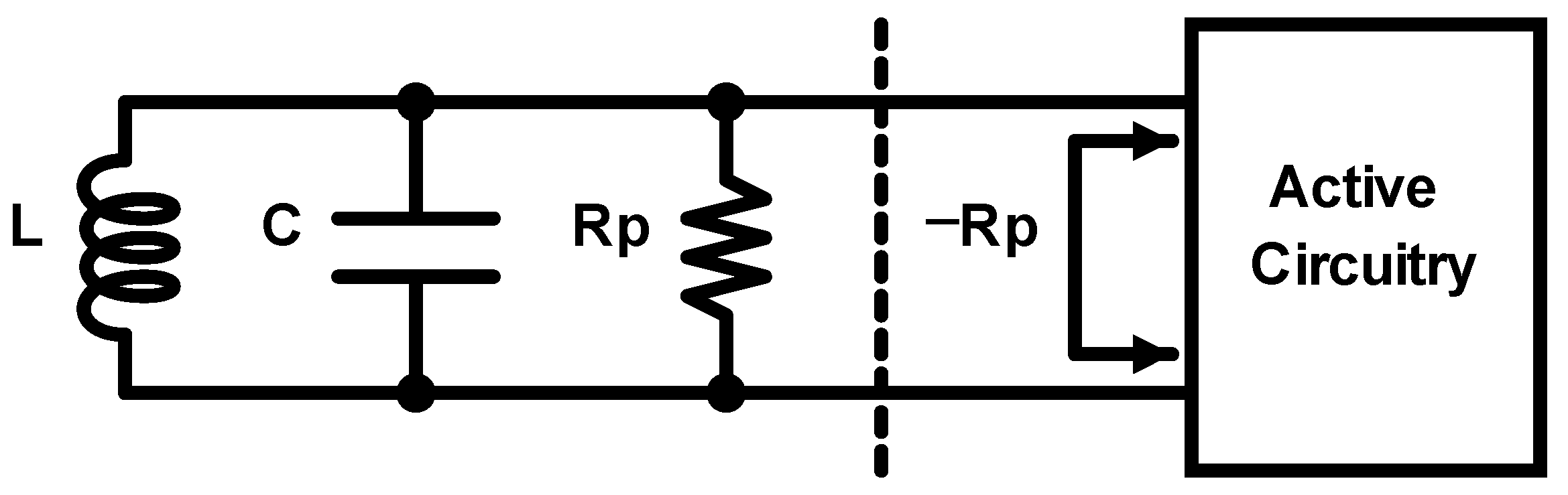
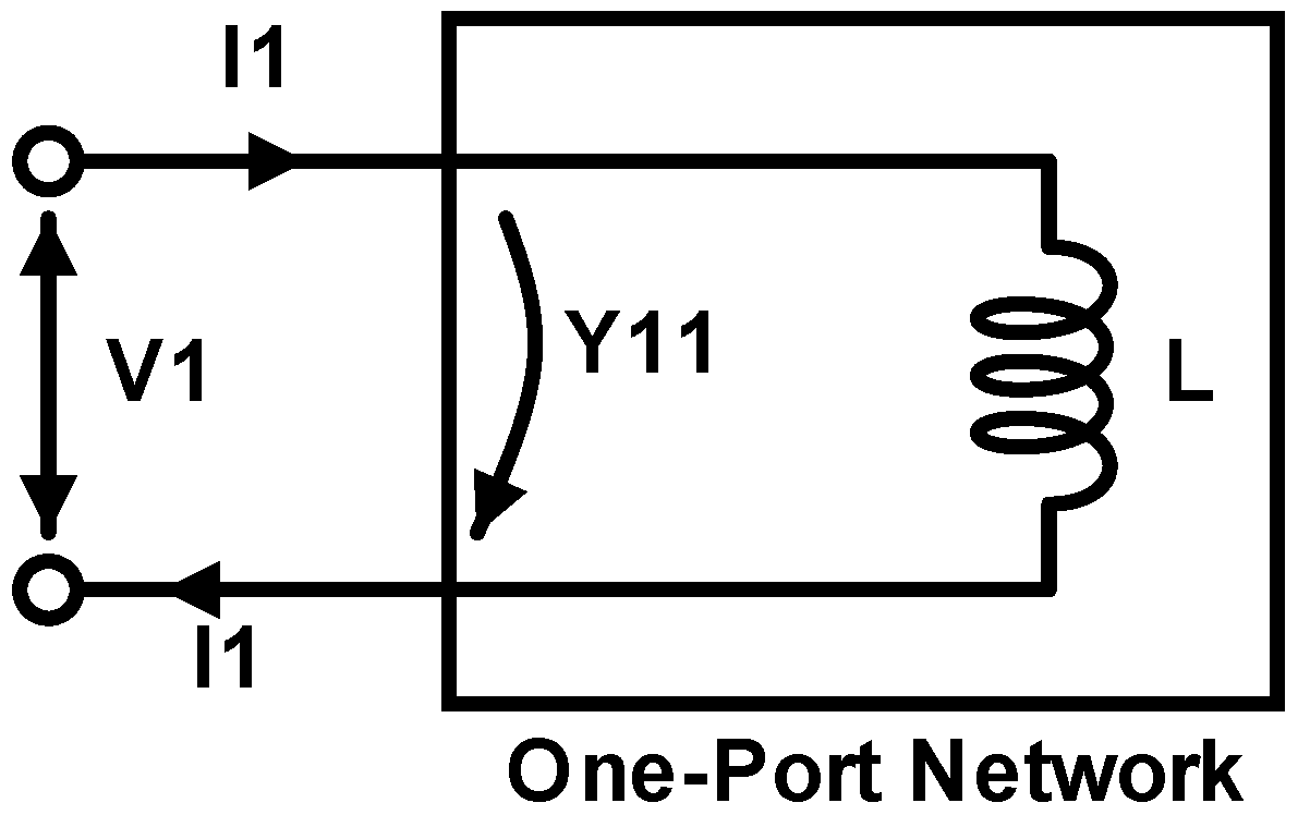
The first step, which involves defining the desired performance specifications, is performed focusing on synthesizing high-performance VCO designs with industry-standard specifications. After setting the initial conditions, the methodology moves to the LC-tank characterization of the VCO. Two processes were included during the execution of the LC-tank characterization: the optimum Q-factor inductor search, which is performed using the cost function, and the LC-tank tuning process via searching the optimum varactor value with which the LC-tank will resonate at the desired frequency of . Finally, the LC-tank characterization procedure finishes by calculating the overall parasitic resistance of the LC-tank using the Z-parameters of its respective one-port network.
Based on the specified requirements and the desired power consumption, the bias current of the VCO is defined. In the topology being tested, the VCO’s biasing is performed utilizing a resistor, simplifying the circuit and improving the phase noise performance [
27]. The bias current emerges as a critical factor influencing key performance metrics of the VCO, such as output voltage amplitude and phase noise [
28]. It is prudent to prioritize setting the bias current, especially when the VCO has a stringent power budget. This approach reduces the number of iterations required in the following stages, speeding up the process of achieving the final specifications. Notably, the output voltage amplitude is directly proportional to the bias current, and this relationship can be expressed as follows:
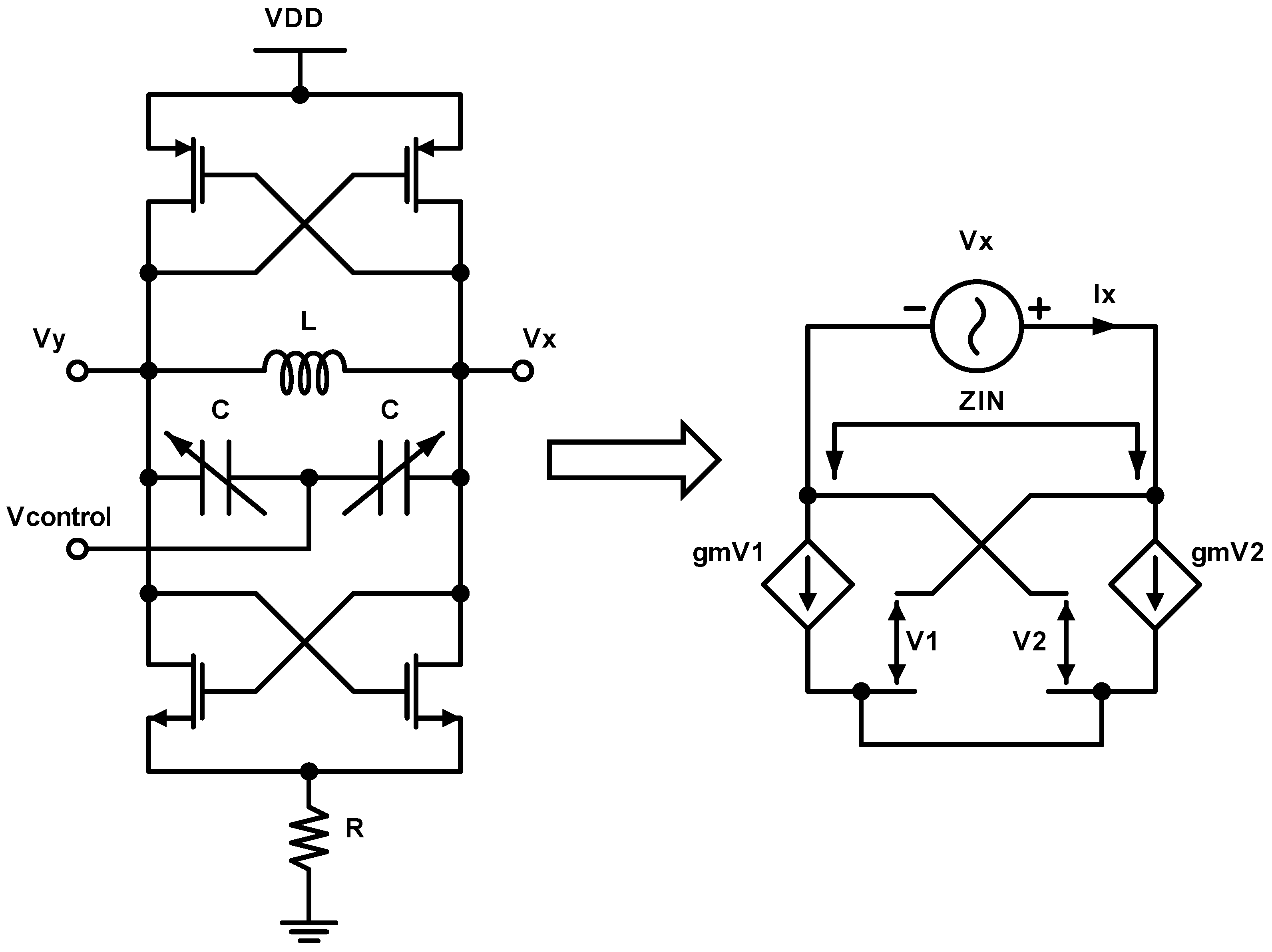
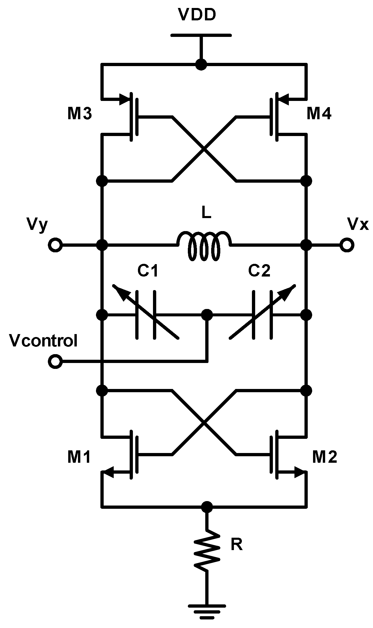
An essential feature of the complementary cross-coupled LC VCO aids in demonstrating this dependency; the presence of both NMOS and PMOS transistors, along with the circuit’s symmetrical structure, results in a doubled output voltage amplitude for the same bias current [
29].
Following the bias definition stage, transistor sizing is performed followed by three consecutive decision loops. Every loop tunes the respective performance metric based on the defined specifications and the required conditions that guarantee oscillation. Initially, the transistors are sized according to the boundary condition for oscillation (17). If this condition is true, the oscillation will occur and the algorithm moves on to the next procedure, which is the output voltage amplitude evaluation. If the output voltage swing is lower than the specified specification, a width increment for both NMOS and PMOS devices is performed, leading to an increase in the transistors’ transconductance to surpass the inverse of the parallel resistance of the tank . It should be noted that the width is increased for both NMOS and PMOS devices, with the aim of keeping the transconductance of both the same. For the process node used in this study, the width ratio is evaluated as .
| Algorithm 2 VCO Design Methodology |
- 1:
Define Min and Max values according to PDK limits: - 2:
Transistor min Channel Width → - 3:
Transistor min Channel Length → - 4:
Minimum Inductor Inner Diameter → - 5:
Maximum Inductor Inner Diameter → - 6:
Minimum Inductor Turns → - 7:
Maximum Inductor Turns → - 8:
MOS VARACTOR min Capacitance → - 9:
MOS VARACTOR max Capacitance → - 10:
- 11:
Define VCO Specifications and Parameters: - 12:
NMOS and PMOS Width ratio for equal → - 13:
Operating Frequency → - 14:
Voltage Supply → - 15:
Bias Current → - 16:
Output Amplitude Swing → - 17:
Phase Noise → - 18:
- 19:
VCO Cost Functions: - 20:
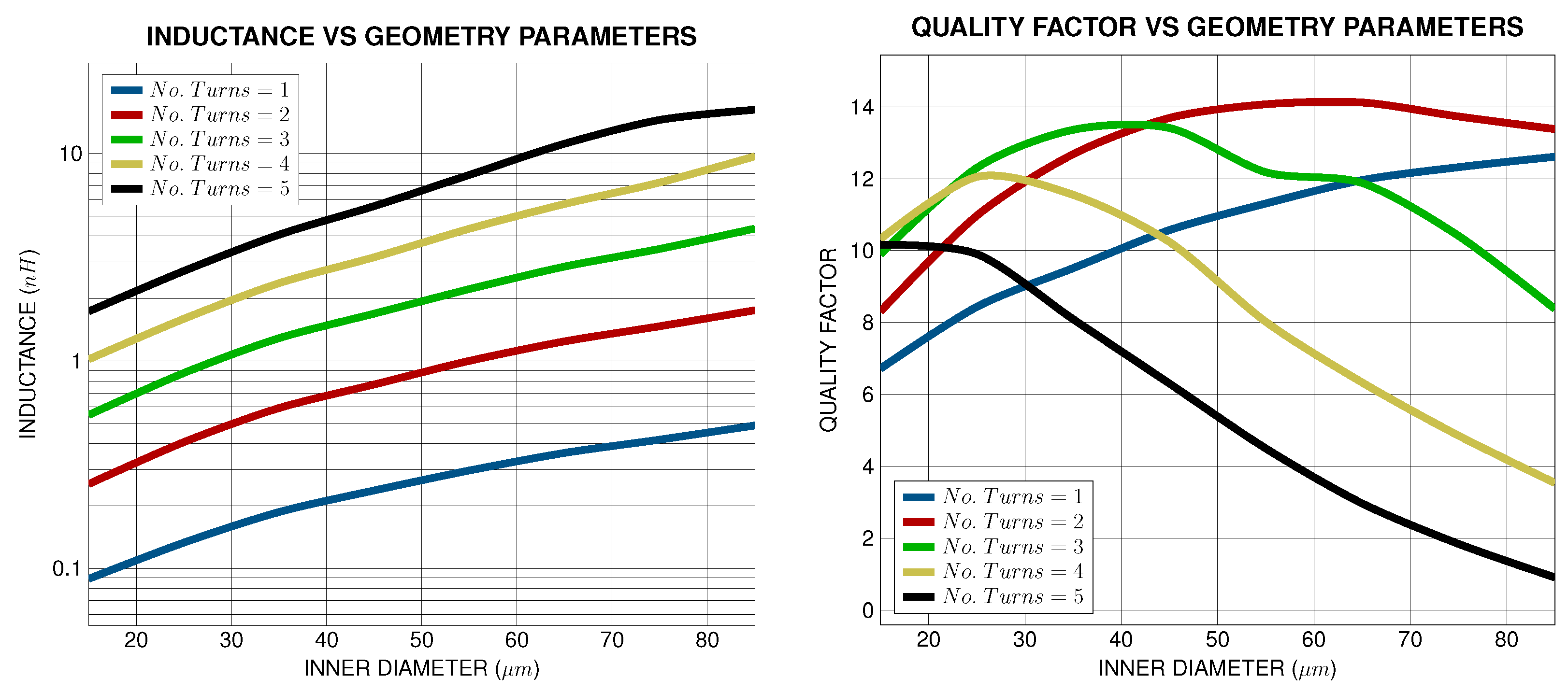
: Returns the Quality Factor of the LC-tank inductor for specific inner diameter and specific number of turns , monitored at the frequency. - 21:
: Returns the maximum real part of the input impedance with respect to frequency. - 22:
: Returns the Inductance of the inductor with specific geometry parameters (inner diameter and number of turns ) at the specified frequency . - 23:
- 24:
Main Optimization Algorithm: - 25:
while (TRUE) { - 26:
// Optimum Inductor Search - 27:
for loop { - 28:
for loop { - 29:
- 30:
return and } - 31:
return } - 32:
// LC-Tank Tuning and Characterization - 33:
for loop { - 34:
if () { - 35:
return } - 36:
return } - 37:
// Transistor Sizing - 38:
define - 39:
while (TRUE) { - 40:
for loop { - 41:
if () { - 42:
if (SATURATION CHECK = TRUE) { - 43:
return break } } } - 44:
else go to define } - 45:
// Output Voltage Swing Tuning - 46:
while (TRUE) { - 47:
for loop { - 48:
if () { - 49:
if (SATURATION CHECK = TRUE) { - 50:
return break } } } - 51:
else go to define } - 52:
// Phase Noise Tuning - 53:
while (TRUE) { - 54:
for loop { - 55:
if () { - 56:
if (SATURATION CHECK = TRUE) { - 57:
return break } } } - 58:
else go to define } - 59:
end
|
In the current topology, resistor-based biasing is employed to set the bias current, rather than using a simple current mirror. However, this approach results in poorly defined current, as it depends on the sizing of the transistors. This dependence arises because the resistor-based configuration does not precisely regulate the current. Consequently, the amplitude of the output voltage can be adjusted by modifying the sizing of the transistors. This relationship underscores the importance of transistor sizing when it comes to achieving the desired output voltage characteristics. If the desired specification is not met, the algorithm returns to the bias current definition procedure to change the bias current of the circuit, thus changing the biasing resistor value.
Finally, the phase noise of the oscillator is evaluated. At this point of the methodology, and taking all the previous steps into consideration, it is possible that the phase noise requirements are met anyway. Nevertheless, few iterations can be made so as to further decrease the phase noise through a loop that increases the width of the transistors, increasing their transconductance. Concluding the description of the presented methodology, it is important to highlight the function of the nested loops present in the three final consecutive iterations, where the circuit’s performance is evaluated. These nested loops are performed extremely fast since they exploit well-defined cost functions about each metric, while they ensure that the transistors remain in the desired region of operation. During the optimization process, if the methodology detects that the transistors have shifted out of the saturation region, it takes corrective action. This correction involves returning to the bias current adjustment step and, by regulating the bias current, the methodology can effectively push the transistors back into the saturation region, ensuring proper operation.


 ,
, 


