

Optimization Study for Enhancing Internal Module Communication Efficiency in Integrated Circuits

Abstract
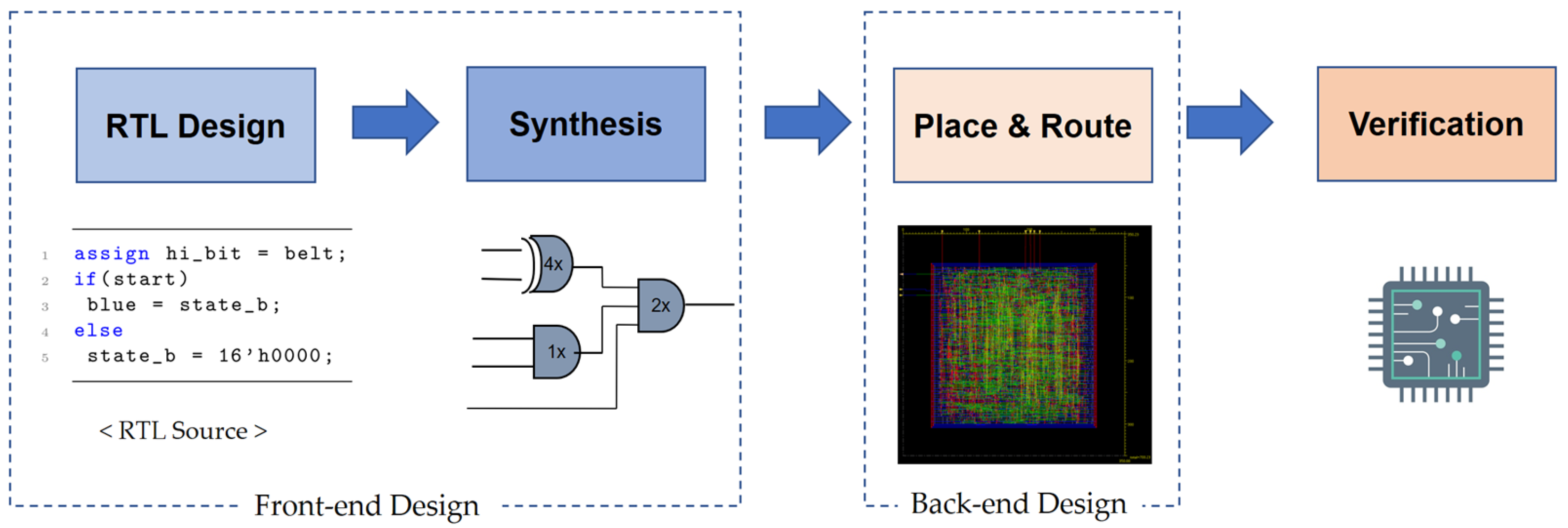
1. Introduction
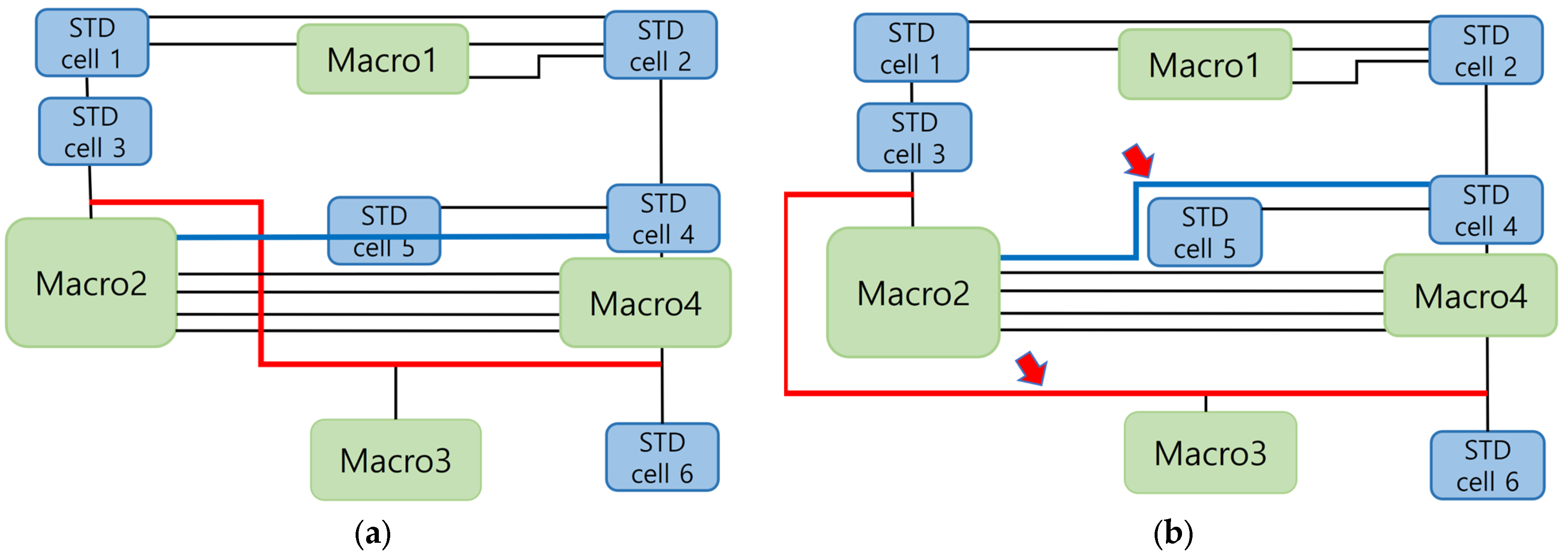
2. Evaluation Metrics—Routing Congestion and Performance
3. Impact and Scope of Front-End Design Elements on Back-End Design
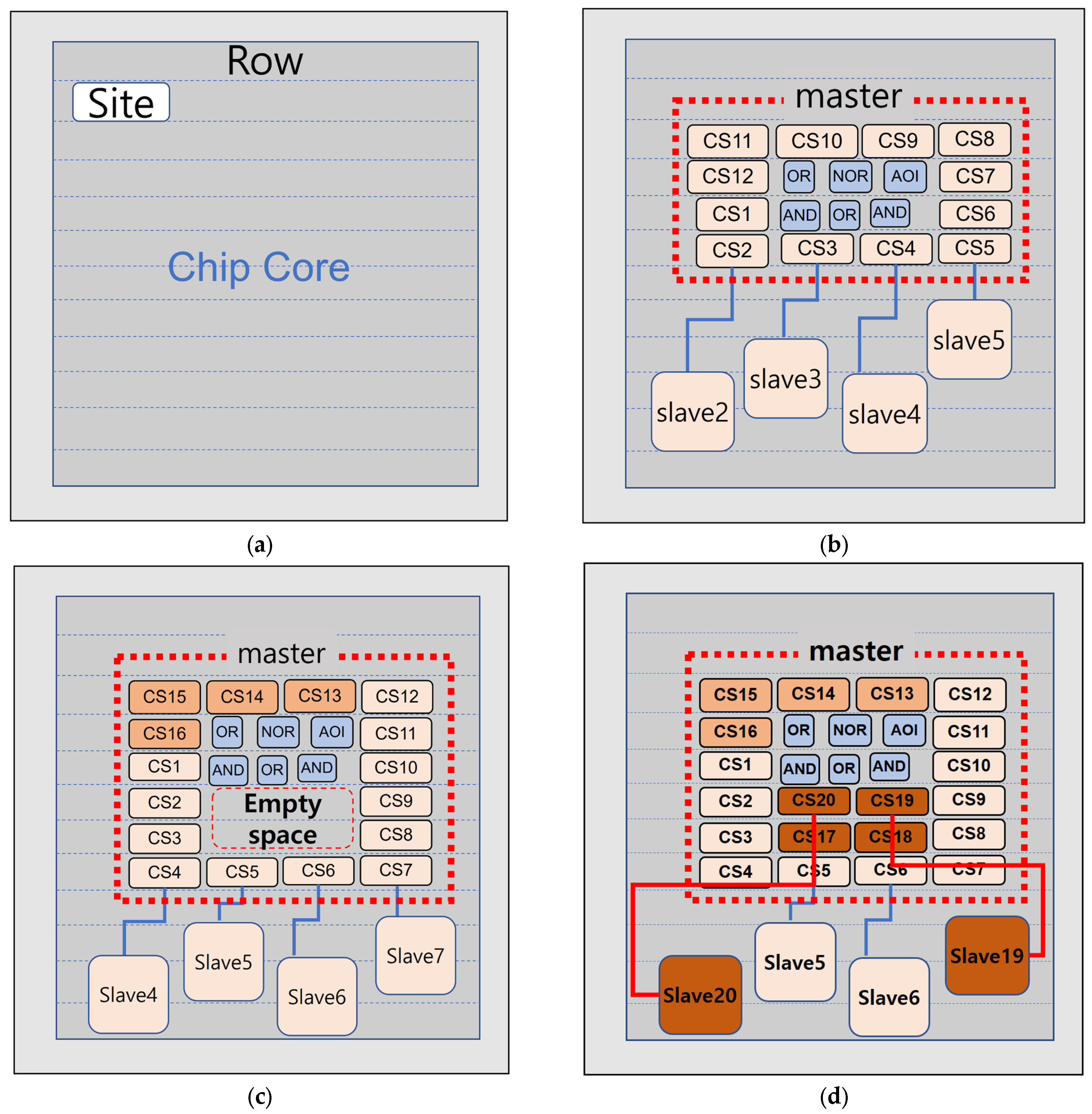
3.1. Area Impact of Increasing CS Registers in a Fixed Primary Module
3.2. Minimum Module Size to Avoid Internal Congestion
4. Experimental Setup and Data Analysis
4.1. Experimental Setup and Methodology
- RTL Simulation Tool: Cadence Xcelium;
- Synthesis Tool: Cadence Genus;
- Place and Routing Tool: Cadence Innovus;
- Library/LEF and Other Process Files Provided by the Foundry (90 nm standard cell process);
- Standard Cell Sizes
- o
- D-flip-flop (1-bit): 11.2 μm (W) × 4 μm (H);
- o
- 2-input NAND Gate: 2 μm (W) × 4 μm (H).
4.2. Routing Congestion and Gate Count Analysis
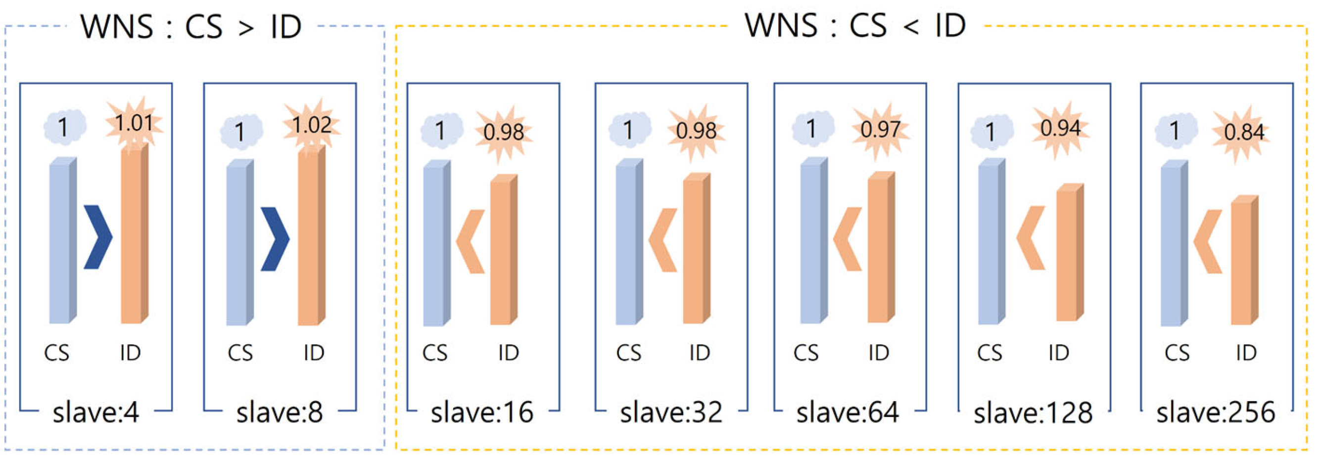
4.3. Evaluation Under Fixed Area Constraints
4.4. Power Consumption Comparison
5. Results
Funding
Data Availability Statement
Conflicts of Interest
References
- Hassoun, S.; Sasao, T. Logic Synthesis and Verification, 1st ed.; Springer: New York, NY, USA, 2002. [Google Scholar]
- Kulkarni, A.M.; Chopde, A. Physical Design: Methodologies and Developments. arXiv 2024, arXiv:240904726. [Google Scholar]
- Golshan, K. Physical Design Essentials; Springer: New York, NY, USA, 2007. [Google Scholar]
- Maity, S.; Jana, S.K. Design of a Power-Performance-Area (PPA) Optimized MOS Current Mode Logic Pre-scaler. Circuits Syst. Signal Process. 2023, 42, 5783–5798. [Google Scholar] [CrossRef]
- Cong, J.; Zhang, Y. Thermal-driven multilevel routing for 3-D ICs. In Proceedings of the 2005 Asia and South Pacific Design Automation Conference, Shanghai, China, 18–21 January 2005; pp. 121–126. [Google Scholar]
- Hu, J.; Sapatnekar, S.S. A timing-constrained algorithm for simultaneous global routing of multiple nets. In Proceedings of the IEEE/ACM International Conference on Computer Aided Design ICCAD-2000 IEEE/ACM Digest of Technical Papers (Cat No 00CH37140), San Jose, CA, USA, 5–9 November 2000; pp. 99–103. [Google Scholar]
- Huang, G.; Hu, J.; He, Y.; Liu, J.; Ma, M.; Shen, Z.; Wu, J.; Xu, Y.; Zhang, H.; Zhong, K. Machine learning for electronic design automation: A survey. ACM Trans. Des. Autom. Electron. Syst. 2021, 26, 1–46. [Google Scholar] [CrossRef]
- Li, L.; Cai, Y.; Zhou, Q. A survey on machine learning-based routing for VLSI physical design. Integration 2022, 86, 51–56. [Google Scholar] [CrossRef]
- Lillis, J.; Cheng, C.-K.; Lin, T.-T. Optimal wire sizing and buffer insertion for low power and a generalized delay model. IEEE J. Solid-State Circuits 1996, 31, 437–447. [Google Scholar] [CrossRef]
- Cohoon, J.; Kairo, J.; Lienig, J. Evolutionary algorithms for the physical design of VLSI circuits. In Advances in Evolutionary Computing: Theory and Applications; Springer: Berlin/Heidelberg, Germany, 2003; pp. 683–711. [Google Scholar]
- Tabrizi, A.F.; Darav, N.K.; Rakai, L.; Kennings, A.; Swartz, W.; Behjat, L. A detailed routing-aware detailed placement technique. In Proceedings of the 2015 IEEE Computer Society Annual Symposium on VLSI, Montpellier, France, 8–10 July 2015; pp. 38–43. [Google Scholar]
- Malhotra, V.M.; Kumar, M.P.; Maheshwari, S.N. An O (|V| 3) algorithm for finding maximum flows in networks. Inf. Process. Lett. 1978, 7, 277–278. [Google Scholar] [CrossRef]
- Achterberg, T.; Koch, T.; Martin, A. Branching rules revisited. Oper. Res. Lett. 2005, 33, 42–54. [Google Scholar] [CrossRef]
- Spindler, P.; Schlichtmann, U.; Johannes, F.M. Abacus: Fast legalization of standard cell circuits with minimal movement. In Proceedings of the 2008 International Symposium on Physical Design, Portland, OR, USA, 13–16 April 2008; pp. 47–53. [Google Scholar]
- Chou, S.; Ho, T.-Y. OAL: An obstacle-aware legalization in standard cell placement with displacement minimization. In Proceedings of the 2009 IEEE International SOC Conference (SOCC), Belfast, UK, 9–11 September 2009; pp. 329–332. [Google Scholar]
- Lee, Y.-M.; Wu, T.-Y.; Chiang, P.-Y. A hierarchical bin-based legalizer for standard-cell designs with minimal disturbance. In Proceedings of the 2010 15th Asia and South Pacific Design Automation Conference (ASP-DAC), Taipei, Taiwan, 18–21 January 2010; pp. 568–573. [Google Scholar]
- Netto, R.; Livramento, V.; Guth, C.; Dos Santos, L.C.; Guntzel, J.L. Speeding up incremental legalization with fast queries to multidimensional trees. In Proceedings of the 2016 IEEE Computer Society Annual Symposium on VLSI (ISVLSI), Pittsburgh, PA, USA, 11–13 July 2016; pp. 36–41. [Google Scholar]
- Lin, Y.; Yu, B.; Xu, X.; Gao, J.-R.; Viswanathan, N.; Liu, W.-H.; Li, Z.; Alpert, C.J.; Pan, D.Z. MrDP: Multiple-row detailed placement of heterogeneous-sized cells for advanced nodes. IEEE Trans. Comput.-Aided Des. Integr. Circuits Syst. 2017, 37, 1237–1250. [Google Scholar] [CrossRef]
- Zhou, Q.; Hu, J.; Zhou, Q. An effective iterative density aware detailed placement algorithm. In Proceedings of the 2014 IEEE International Symposium on Circuits and Systems (ISCAS), Melbourne, VIC, Australia, 1–5 June 2014. pp. 1444–1447.
- Amuru, D.; Zahra, A.; Vudumula, H.V.; Cherupally, P.K.; Gurram, S.R.; Ahmad, A.; Abbas, Z. AI/ML algorithms and applications in VLSI design and technology. Integration 2023, 93, 102048. [Google Scholar] [CrossRef]
- Ren, H.; Godil, S.; Khailany, B.; Kirby, R.; Liao, H.; Nath, S.; Raiman, J.; Roy, R. Optimizing vlsi implementation with reinforcement learning-iccad special session paper. In Proceedings of the 2021 IEEE/ACM International Conference on Computer Aided Design (ICCAD), Munich, Germany, 1–4 November 2021; pp. 1–6. [Google Scholar]
- Ho, C.-T.; Chandna, A.; Guan, D.; Ho, A.; Kim, M.; Li, Y.; Ren, H. Novel Transformer Model Based Clustering Method for Standard Cell Design Automation. In Proceedings of the 2024 International Symposium on Physical Design, Taipei Taiwan, 12–15 March 2024; pp. 195–203. [Google Scholar]
- Monteiro, J.L. Algorithms to Improve Area Density Utilization, Routability and Timing During Detailed Placement and Legalization of VLSI Circuits. 2019. Available online: https://lume.ufrgs.br/handle/10183/197078 (accessed on 4 May 2025).
- Cheng, W.-K.; Guo, Y.-Y.; Wu, C.-S. Evaluation of routability-driven macro placement with machine-learning technique. In Proceedings of the 2018 7th International Symposium on Next Generation Electronics (ISNE), Taipei, Taiwan, 7–9 May 2018. pp. 1–3.
- Liu, S.; Sun, Q.; Liao, P.; Lin, Y.; Yu, B. Global placement with deep learning-enabled explicit routability optimization. In Proceedings of the 2021 Design, Automation & Test in Europe Conference & Exhibition (DATE), Grenoble, France, 1–5 February 2021; pp. 1821–1824. [Google Scholar]
- Cheng, W.-K.; Wu, C.-S. Machine Learning Techniques for Building and Evaluation of Routability-driven Macro Placement. In Proceedings of the 2019 IEEE International Conference on Consumer Electronics-Taiwan (ICCE-TW), Yilan, Taiwan, 20–22 May 2019; pp. 1–2. [Google Scholar]
- Chen, J.; Kuang, J.; Zhao, G.; Huang, D.J.-H.; Young, E.F. PROS: A plug-in for routability optimization applied in the state-of-the-art commercial EDA tool using deep learning. In Proceedings of the 39th International Conference on Computer-Aided Design, Virtual, 2–5 November 2020; pp. 1–8. [Google Scholar]
- Wang, B.; Shen, G.; Li, D.; Hao, J.; Liu, W.; Huang, Y.; Wu, H.; Lin, Y.; Chen, G.; Heng, P.A. LHNN: Lattice hypergraph neural network for VLSI congestion prediction. In Proceedings of the 59th ACM/IEEE Design Automation Conference, San Francisco, CA, USA, 10–14 July 2022; pp. 1297–1302. [Google Scholar]
- Tabrizi, A.F.; Darav, N.K.; Xu, S.; Rakai, L.; Bustany, I.; Kennings, A.; Behjat, L. A machine learning framework to identify detailed routing short violations from a placed netlist. In Proceedings of the 55th Annual Design Automation Conference, San Francisco, CA, USA, 24–29 June 2018; pp. 1–6. [Google Scholar]
- Lu, Y.-C.; Lee, J.; Agnesina, A.; Samadi, K.; Lim, S.K. GAN-CTS: A generative adversarial framework for clock tree prediction and optimization. In Proceedings of the 2019 IEEE/ACM International Conference on Computer-Aided Design (ICCAD), Westminster, CO, USA, 4–7 November 2019; pp. 1–8. [Google Scholar]
- Xu, J.; Hong, X.; Jing, T.; Zhang, L.; Gu, J. A coupling and crosstalk-considered timing-driven global routing algorithm for high-performance circuit design. Integration 2006, 39, 457–473. [Google Scholar] [CrossRef]


| Number of Target Modules | 4 | 8 | 16 | 32 | 64 | 128 | 256 | Unit |
|---|---|---|---|---|---|---|---|---|
| Total Gates | 41 | 54 | 78 | 121 | 200 | 351 | 646 | gate |
| FF Count | 11 | 15 | 23 | 39 | 71 | 135 | 263 | gate |
| Other Logic Gates | 30 | 39 | 55 | 82 | 129 | 216 | 383 | gate |
| Area-Normalized FF Count (×6 logic size) | 66 | 90 | 138 | 234 | 426 | 810 | 1578 | gate |
| FF Area Ratio | 68.75 | 69.8 | 71.5 | 74.1 | 76.8 | 78.9 | 80.5 | % |
| Number of Target Modules | 4 | 8 | 16 | 32 | 64 | 128 | 256 | Unit | |
|---|---|---|---|---|---|---|---|---|---|
| Synthesis | Gate | 494 | 977 | 1943 | 3857 | 7442 | 14,612 | 28,944 | gate |
| Area | 15,076 | 29,889 | 59,452 | 118,884 | 235,670 | 468,555 | 934,302 | ||
| Rate of Increase | - | 1.98 | 1.98 | 1.99 | 1.98 | 1.98 | 1.99 | % | |
| P&R | Width | 149 | 209 | 295 | 416 | 584 | 820 | 1158 | |
| Height | 144 | 204 | 288 | 408 | 576 | 816 | 1148 | ||
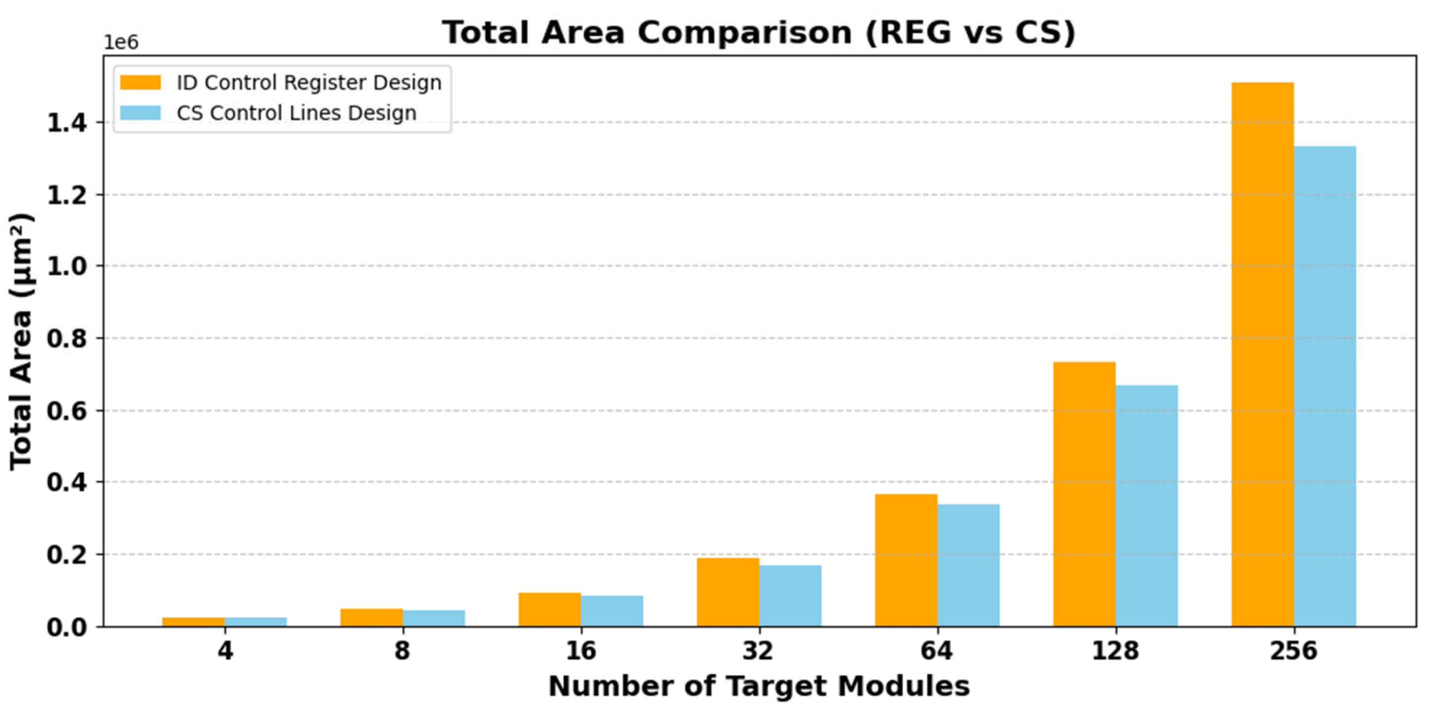
| Area (w × h) | 21,542 | 42,758 | 85,017 | 169,891 | 336,844 | 669,446 | 1,330,302 | ||
| Rate of Increase | - | 1.98 | 1.98 | 1.99 | 1.98 | 1.98 | 1.98 | % | |
| Result | Routes Required | 509 | 999 | 1982 | 3929 | 7706 | 15,257 | 30,355 | count |
| Routes to Avoid | 140 | 274 | 563 | 1141 | 2274 | 5118 | 9109 | count | |
| Routing Congestion | 0.275 | 0.274 | 0.284 | 0.290 | 0.295 | 0.335 | 0.300 | - | |
| Number of Target Modules | 4 | 8 | 16 | 32 | 64 | 128 | 256 | Unit | |
|---|---|---|---|---|---|---|---|---|---|
| Synthesis | Gate | 526 | 1010 | 2122 | 4378 | 8388 | 16,692 | 35,094 | gate |
| Area | 16,024 | 31,768 | 64,638 | 130,825 | 256,379 | 510,194 | 1,055,970 | ||
| Rate of Increase | - | 1.98 | 1.99 | 1.99 | 1.98 | 1.98 | 1.99 | % | |
| P&R | Width | 154 | 214 | 308 | 436 | 606 | 855 | 1236 | |
| Height | 148 | 212 | 300 | 428 | 604 | 854 | 1220 | ||
| Area (w × h) | 22,910 | 45,452 | 92,400 | 186,950 | 366,265 | 730,511 | 1,508,896 | ||
| Rate of Increase | - | 1.98 | 1.99 | 1.99 | 1.98 | 1.99 | 1.99 | % | |
| Result | Routes Required | 555 | 1088 | 2193 | 4514 | 8833 | 17,820 | 36,380 | count |
| Routes to Avoid | 161 | 302 | 595 | 1224 | 2386 | 4830 | 10,304 | count | |
| Routing Congestion | 0.29 | 0.277 | 0.271 | 0.271 | 0.271 | 0.271 | 0.28 | - | |
| Number of Target Modules | 4 | 8 | 16 | 32 | 64 | 128 | 256 | Unit | |
|---|---|---|---|---|---|---|---|---|---|
| Synthesis | Gate | 526 | 1010 | 2122 | 4378 | 8388 | 16,692 | 35,094 | gate |
| Area | 16,024 | 31,768 | 64,638 | 130,825 | 256,379 | 510,194 | 1,055,970 | ||
| Rate of Increase | - | 1.98 | 1.99 | 1.99 | 1.98 | 1.98 | 1.99 | % | |
| P&R | Width | 149 | 209 | 295 | 416 | 584 | 820 | 1158 | |
| Height | 144 | 204 | 288 | 408 | 576 | 816 | 1148 | ||
| Routing Congestion | 0.29 | 0.277 | 0.271 | 0.271 | 0.271 | 0.271 | 0.28 | - | |
| Number of Target Modules | 4 | 8 | 16 | 32 | 64 | 128 | 256 | Unit |
|---|---|---|---|---|---|---|---|---|
| Leakage | 11.6 | 23 | 46.7 | 94.7 | 187.6 | 387.8 | 775.3 | μW |
| Internal | 9.9 | 16.3 | 30.1 | 56.7 | 106.3 | 217.9 | 434.6 | μW |
| Switching | 11.5 | 18.9 | 35.6 | 68.4 | 128.7 | 270.4 | 607.8 | μW |
| Total | 33 | 58.2 | 112.4 | 219.8 | 422.6 | 876.1 | 1817.7 | μW |
Disclaimer/Publisher’s Note: The statements, opinions and data contained in all publications are solely those of the individual author(s) and contributor(s) and not of MDPI and/or the editor(s). MDPI and/or the editor(s) disclaim responsibility for any injury to people or property resulting from any ideas, methods, instructions or products referred to in the content. |
© 2025 by the author. Licensee MDPI, Basel, Switzerland. This article is an open access article distributed under the terms and conditions of the Creative Commons Attribution (CC BY) license (https://creativecommons.org/licenses/by/4.0/).
Share and Cite
Seo, J.-H. Optimization Study for Enhancing Internal Module Communication Efficiency in Integrated Circuits. Electronics 2025, 14, 2661. https://doi.org/10.3390/electronics14132661
Seo J-H. Optimization Study for Enhancing Internal Module Communication Efficiency in Integrated Circuits. Electronics. 2025; 14(13):2661. https://doi.org/10.3390/electronics14132661
Chicago/Turabian StyleSeo, Jong-Hyun. 2025. "Optimization Study for Enhancing Internal Module Communication Efficiency in Integrated Circuits" Electronics 14, no. 13: 2661. https://doi.org/10.3390/electronics14132661
APA StyleSeo, J.-H. (2025). Optimization Study for Enhancing Internal Module Communication Efficiency in Integrated Circuits. Electronics, 14(13), 2661. https://doi.org/10.3390/electronics14132661