Article

Hybrid Radio-Frequency-Energy- and Solar-Energy-Harvesting-Integrated Circuit for Internet of Things and Low-Power Applications

Department of Electrical Engineering, National Taipei University of Technology, Taipei 10608, Taiwan
*
Author to whom correspondence should be addressed.
Electronics 2025, 14(11), 2192; https://doi.org/10.3390/electronics14112192
Submission received: 23 April 2025 / Revised: 25 May 2025 / Accepted: 26 May 2025 / Published: 28 May 2025

Abstract

:
This paper proposes a hybrid energy-harvesting chip that utilizes both radio-frequency (RF) energy and solar energy for low-power applications and extended service life. The key contributions include a wide input power range, a compact chip area, and a high maximum power conversion efficiency (PCE). Solar energy is a clean and readily available source. The hybrid energy harvesting system has gained popularity by combining RF and solar energy to improve overall energy availability and efficiency. The proposed chip comprises a matching network, rectifier, charge pump, DC combiner, overvoltage protection circuit, and low-dropout voltage regulator (LDO). The matching network ensures maximum power delivery from the antenna to the rectifier. The rectifier circuit utilizes a cross-coupled differential drive rectifier to convert radio frequency energy into DC voltage, incorporating boosting functionality. In addition, a solar harvester is employed to provide an additional energy source to extend service time and stabilize the output by combining it with the radio-frequency source using a DC combiner. The overvoltage protection circuit safeguards against high voltage passing from the DC combiner to the LDO. Finally, the LDO facilitates the production of a stable output voltage. The entire circuit is simulated using the Taiwan Semiconductor Manufacturing Company 0.18 µm 1P6M complementary metal–oxide–semiconductor standard process developed by the Taiwan Semiconductor Research Institute. The simulation results indicated a rectifier conversion efficiency of approximately 41.6% for the proposed radio-frequency-energy-harvesting system. It can operate with power levels ranging from −1 to 20 dBm, and the rectifier circuit’s output voltage is within the range of 1.7–1.8 V. A 0.2 W monocrystalline silicon solar panel (70 × 30 mm2) was used to generate a supplied voltage of 1 V. The overvoltage protection circuit limited the output voltage to 3.6 V. Finally, the LDO yielded a stable output voltage of 3.3 V.

1. Introduction

Energy consumption and the use of wireless mobile networks have skyrocketed over the past two decades due to population growth and economic development [1]. Consequently, affordable and low-power radio-frequency (RF) integrated circuits are in high demand because of their central role in wireless communication systems [2]. These circuits are designed in the form of integrated, multifunctional systems-on-a-chip. Research on this topic has mainly focused on understanding the design fundamentals of RF integrated circuits and exploring the outcomes of combining these circuits with other charging sources to gain insights into their operation, particularly when used as wireless transceiver integrated circuits [3]. Previous studies have analyzed various components of RF-integrated circuits, such as voltage-controlled oscillators, mixers, and low-noise amplifiers. Studies have also examined the challenges involved in the testing of hybrid energy-harvesting systems (HEHSs) [4].
A complementary metal–oxide–semiconductor (CMOS) power management system was presented with wide-range RF for ultra-high-frequency wireless energy harvesting. This system uses a power-aware rectifier and operates based on an adaptive DC–DC conversion ratio to scavenge energy efficiently and avoid sudden power loss due to environmental disturbance. At high input power (greater than −9 dBm), the proposed architecture improved efficiency by approximately 15% compared with a system comprising a conventional rectifier followed by a linear regulator [5]. In a subsequent study, a Dickson voltage multiplier was adopted as the RF voltage rectifier, and a buck–boost converter was used as the DC combiner. The output DC voltage was programmable, and the harvesting system was fabricated using a 0.18 µm CMOS process [6].
A technical comparison with alternative converter topologies is provided here to clarify the rationale behind the selected approach. Alternative techniques such as boost, flyback, and single-ended primary inductor converter (SEPIC) topologies utilize inductors to form their respective converter structures. Inductors are typically more suitable for off-chip applications, particularly in large-scale energy-harvesting systems. However, they are difficult to implement in standard CMOS processes due to their large on-chip area requirements and high parameter variation. According to a search conducted in the IEEE Xplore Digital Library, only one conference paper employing the flyback converter for energy harvesting applications was published in 2014 [7]. In contrast, 194 papers have been published on RF energy-harvesting systems using boost converters between 2006 and 2025 [8], indicating the widespread adoption of the boost converter in RF energy-harvesting integrated circuits. With regard to the SEPIC converter, a total of 329 papers have been published across various research domains. However, none of them reported the integration of a SEPIC converter with an RF energy-harvesting system [9]. In summary, although the boost converter is considered suitable for RF energy harvesting applications, both flyback and SEPIC converters require further investigation to determine their viability in this context. Nevertheless, this study did not adopt the boost converter due to its large chip area and high variability. Instead, a three-stage cross-coupled differential-drive (CCDD) rectifier circuit was employed, consisting of six NMOSFETs and six PMOSFETs [10].
A recent study proposed a hybrid RF/solar energy-scavenging system composed of a highly efficient dual-band RF energy harvester coupled with a solar cell. A Schottky diode (SMS-7630) was used as a rectifying element, and a monocrystalline solar cell (SLMD121H10L) was used for harvesting solar energy [11]. In a subsequent study, a solar cell and antenna, which is capable of harvesting ambient electromagnetic energy, were combined in a hybrid energy-harvesting circuit [12]. A hybrid RF–solar energy harvester was engineered on the basis of a newly designed RF energy harvester and an off-the-shelf solar panel with a boost converter [13]. A flexible and wearable hybrid RF–solar energy-harvesting system was proposed for powering wearable electronic devices. This harvesting system comprises a flexible transparent antenna, a flexible transparent rectifying circuit, and an amorphous silicon solar cell [14]. A power harvester with a Schottky diode and a photodiode was designed to cooperatively harvest ambient RF and solar energy [15]. The next generation of devices can sustain themselves without a battery by harvesting energy. An energy-harvesting design and analysis model is thus presented to collect solar and RF energy and store it for wireless sensor network applications. The viability of the model was assessed using two microcontroller-based implementations [16]. The following section describes the circuit implementation of the HEHS. Simulation results are presented in Section 3, and the conclusions are presented in Section 4.

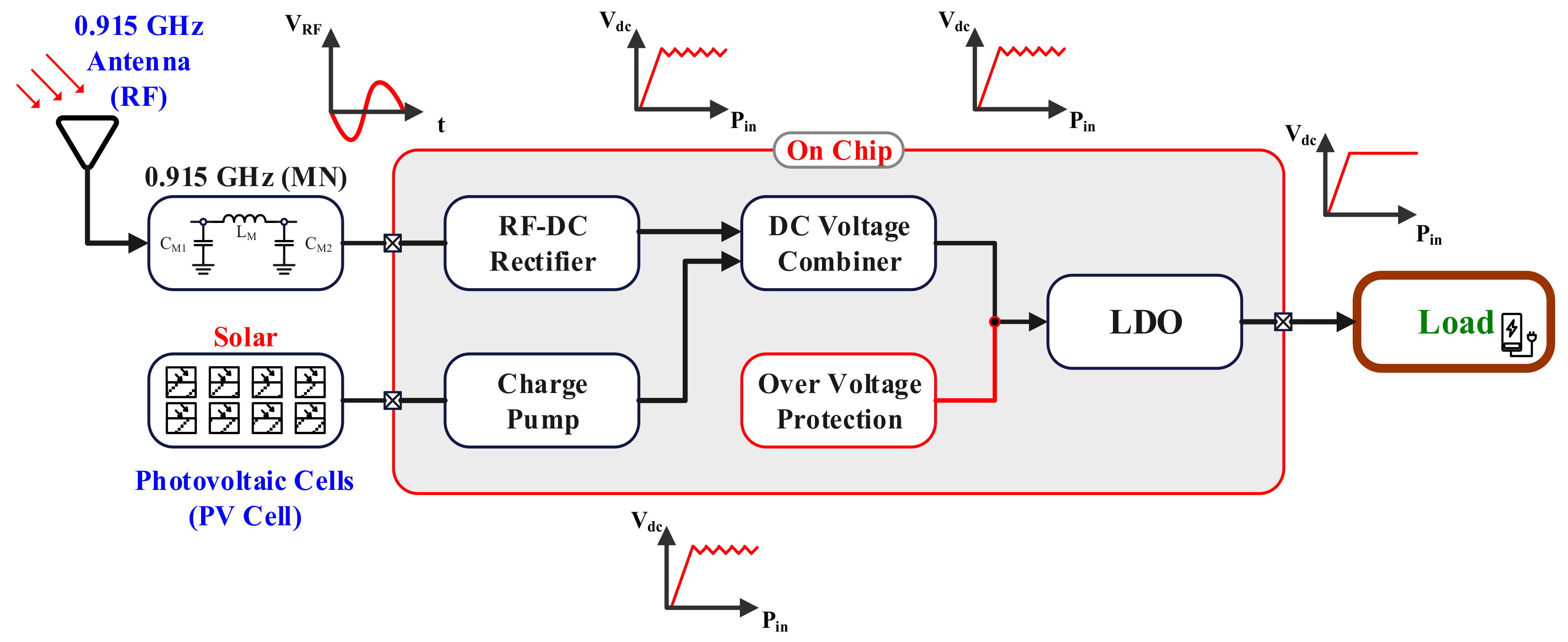
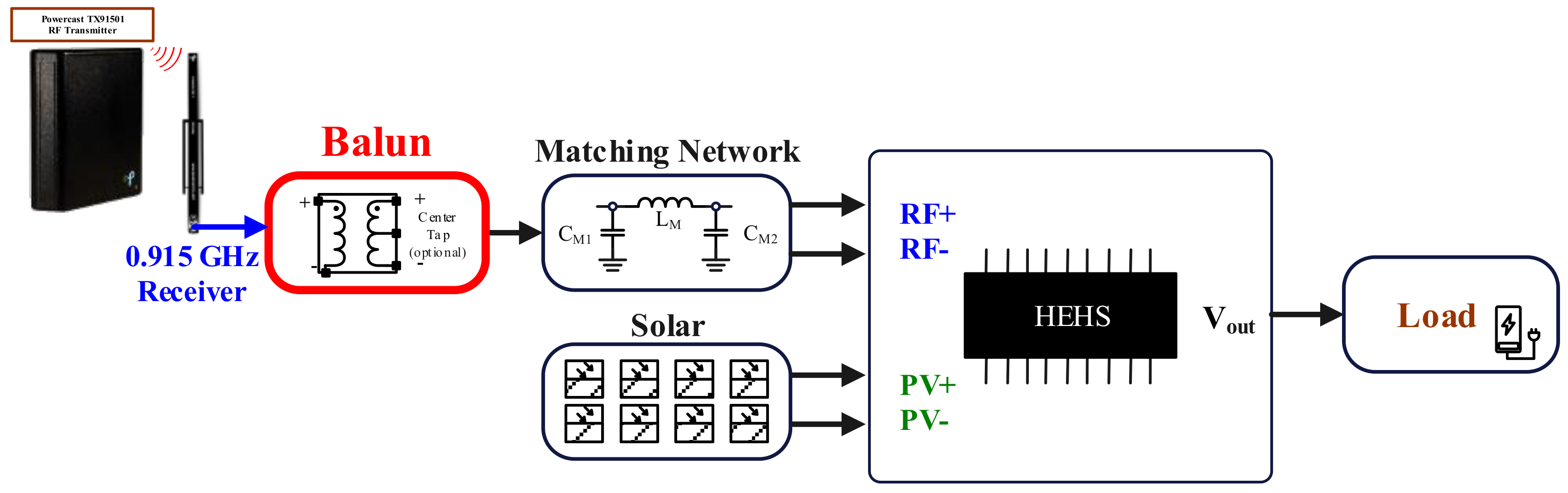
2. Circuit Implementation of Hybrid Energy-Harvesting System

Figure 1 illustrates the architecture of the proposed HEHS, comprising a matching network, an RF–DC rectifier, a charge pump, a DC voltage combiner, an overvoltage protection (OVP) circuit, and a low-dropout linear voltage regulator (LDO) [17]. The HEHS receives RF signals through the antenna at a frequency of 0.915 GHz, Powercast Model TX91501, Taipei City, Taiwan. First, the balun (Murata, Kyoto, Japan) and matching network convert the RF signal into a differential signal to maximize power transformation. The RF–DC rectifier circuit converts the RF signal into a DC voltage. Meanwhile, an additional energy source (solar) is fed to the HEHS to serve as a secondary supply voltage. The charge pump circuit converts the applied solar energy into a DC voltage. The two converted DC voltages are merged by the DC voltage combiner. An OVP circuit is connected to the output of the DC voltage combiner to offer protection from overvoltage. Finally, the LDO generates a stable DC voltage for applications related to the Internet of Things and low-power applications. In this system, the RF energy is always low because it is received through the antenna; by contrast, the solar energy is stable and of greater use to the system.

2.1. Balun’s Function

The RF antenna only transmits a single-ended signal; therefore, a balun converts the received single-ended signal into a differential signal. Figure 2 highlights the position of the balun used in the HEHS: between the antenna and the matching network. A loss of conversion efficiency of approximately 10% is incurred at the balun (Figure 2). Furthermore, the input impedance is prone to variations because of the microstrip line and also because the balun is expected to provide information on the impedance ratio. The actual impact of the balun on the chip must be measured online, and the simulated input impedance of the antenna must be 50 Ω.

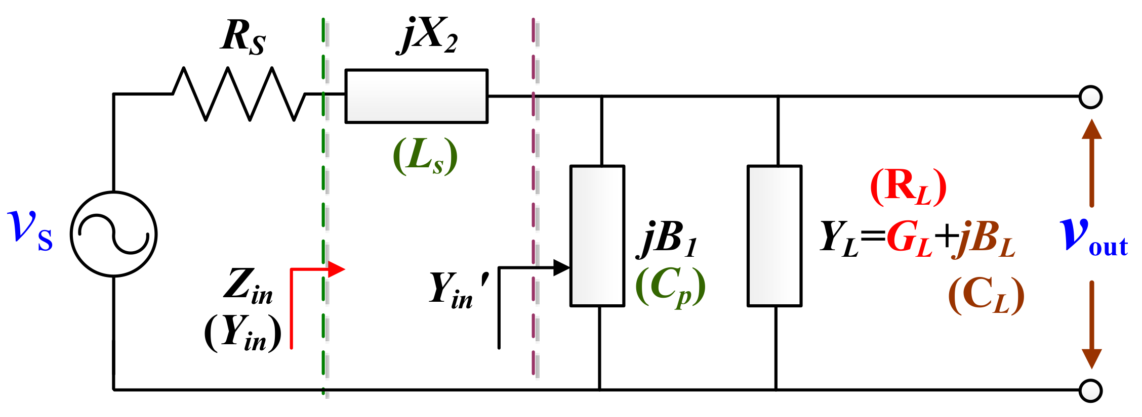
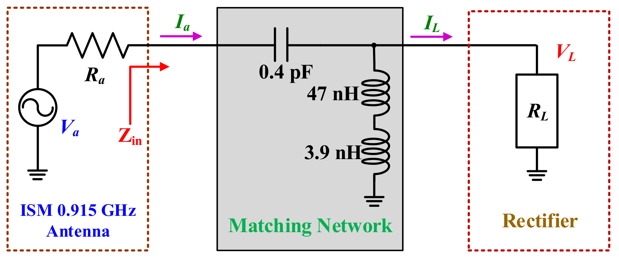
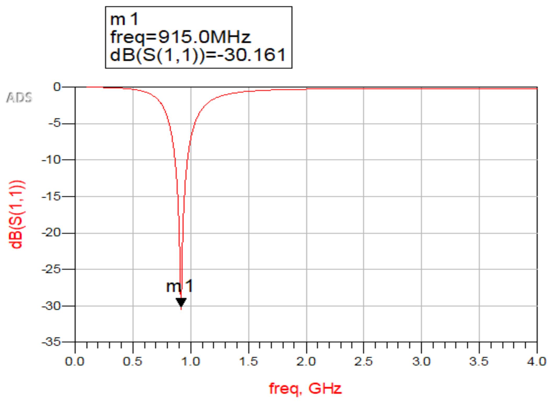
2.2. Matching Network

A matching network is crucial because it guarantees that the system’s input impedance matches the antenna’s impedance of 50 Ω. The RF energy-harvesting system operates at a frequency of 0.915 GHz, which must be appropriately matched with the impedance of 50 Ω. The matching network is completed using capacitors and inductors (Murata Manufacturing, Kyoto, Japan). The matching network ensures optimal power transfer from the antenna to the rectifier and facilitates an increase in the voltage to minimize energy loss and enhance overall conversion efficiency. Figure 3 shows an ideal impedance conversion component that couples the load YL to the input impedance Zin. For simplification, all components are assumed to be loss-free [2]. If the input voltage vS is sinusoidal, then the input signal can be expressed in terms of the peak voltage Vs as follows:
v s = V s cos ω t
The input and output powers can be expressed as follows:
P i n = 1 2 × Z i n R s + Z i n × v s 2 × e Y i n = 1 2 1 1 + Y i n R s 2 v s 2 e Y i n
P o u t = 1 2 v o u t 2 e Y L
where vs and vout represent magnitudes of the input and output voltages, respectively; RS represents the internal resistance of the input source; Yin represents input conductance; YL represents load conductance; and ℜe is the real part operator.
Suppose the input impedance Zin is matched to the internal resistance Rs (Zin = 1/Yin = Rs), and the input power is completely transmitted to the output power (Pin = Pout). In that case, the relationship between vout and vs can be expressed as follows:
1 8 v s 2 e Y i n = 1 2 v o u t 2 e Y L v o u t v s = 1 2 e Y i n e Y L
As shown in Figure 3, the input impedance Zin can be expressed as follows:
Z i n = j X 2 + 1 Y i n ' = j X 2 + 1 j B 1 + G L + j B L = G L j B 1 + B L + j X 2 G L 2 + B 1 + B L 2 G L 2 + B 1 + B L 2
and
v o u t v s = 1 2 e Y i n e Y L = 1 2 G L 2 + B 1 + B L 2 G L G L = 1 2 1 + B 1 + B L G L 2
where jX2 and jB1 represent the impedance of the series inductor (Ls) and the susceptance of the parallel capacitor (Cp), respectively, in the L-section matching network. Similarly, GL and jBL denote the conductance of the parallel resistor (RL) and the susceptance of the parallel capacitor (CL), respectively, in the load.
Figure 4 illustrates the matching network, which is located between the antenna and the N-channel metal–oxide–semiconductor (NMOS) rectifier. The impedance of the Industrial, Scientific, and Medical (ISM) 0.915-GHz antenna is approximately 50 Ω, whereas the input impedance of the three-stage modified NMOS rectifier is equal to 50 × (0.427 − j × 3.102) Ω. A matching network of (28.71 − j × 154.2) Ω is added to guarantee that the input impedance Zin of the rectifier with the matching network is approximately 50 Ω. The matching network, composed of an inductor (LQG15HS_02, Murata Manufacturing) and a capacitor (GRM15, Murata Manufacturing), is simulated using ADS software (2023 Product, Keysight, Santa Rosa, CA, USA).

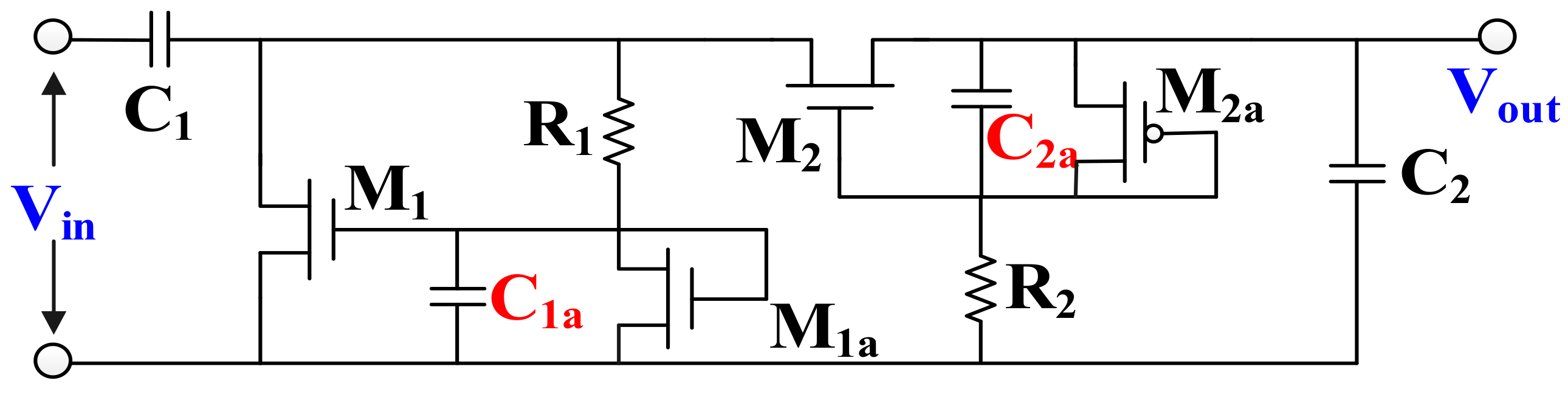
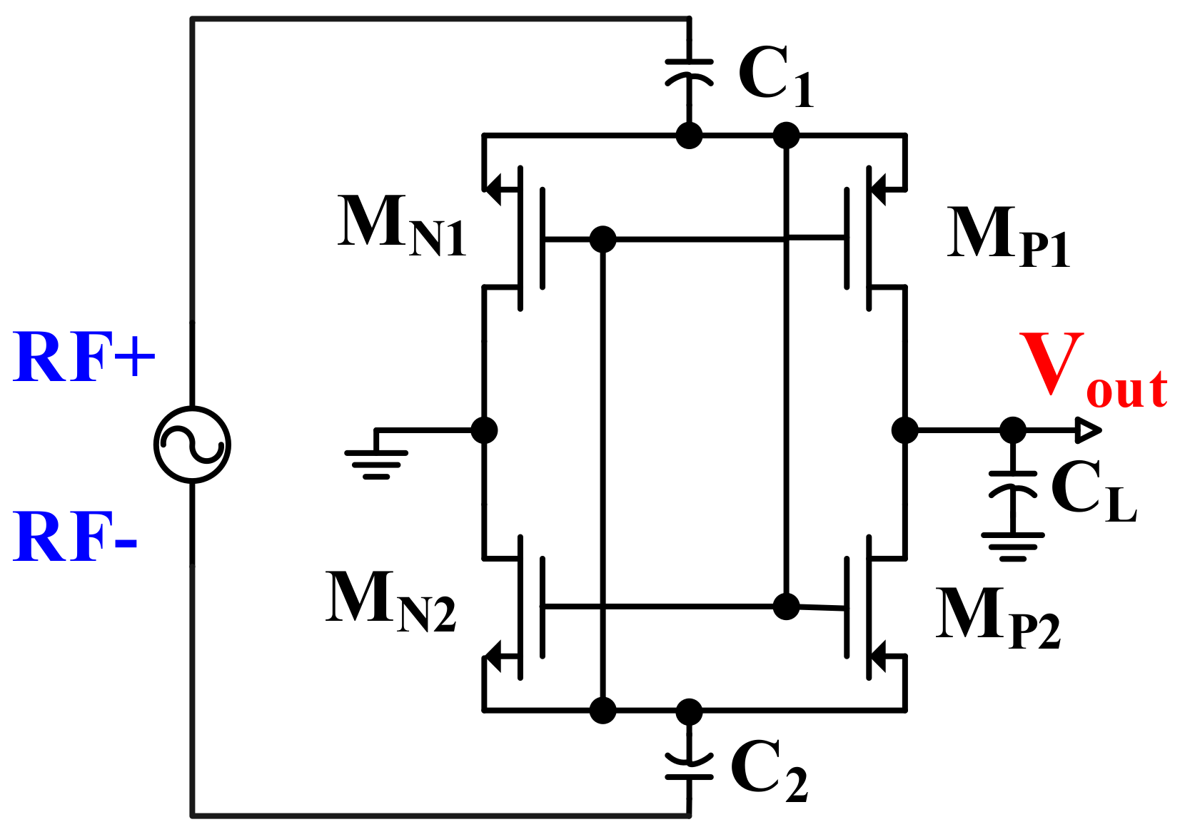
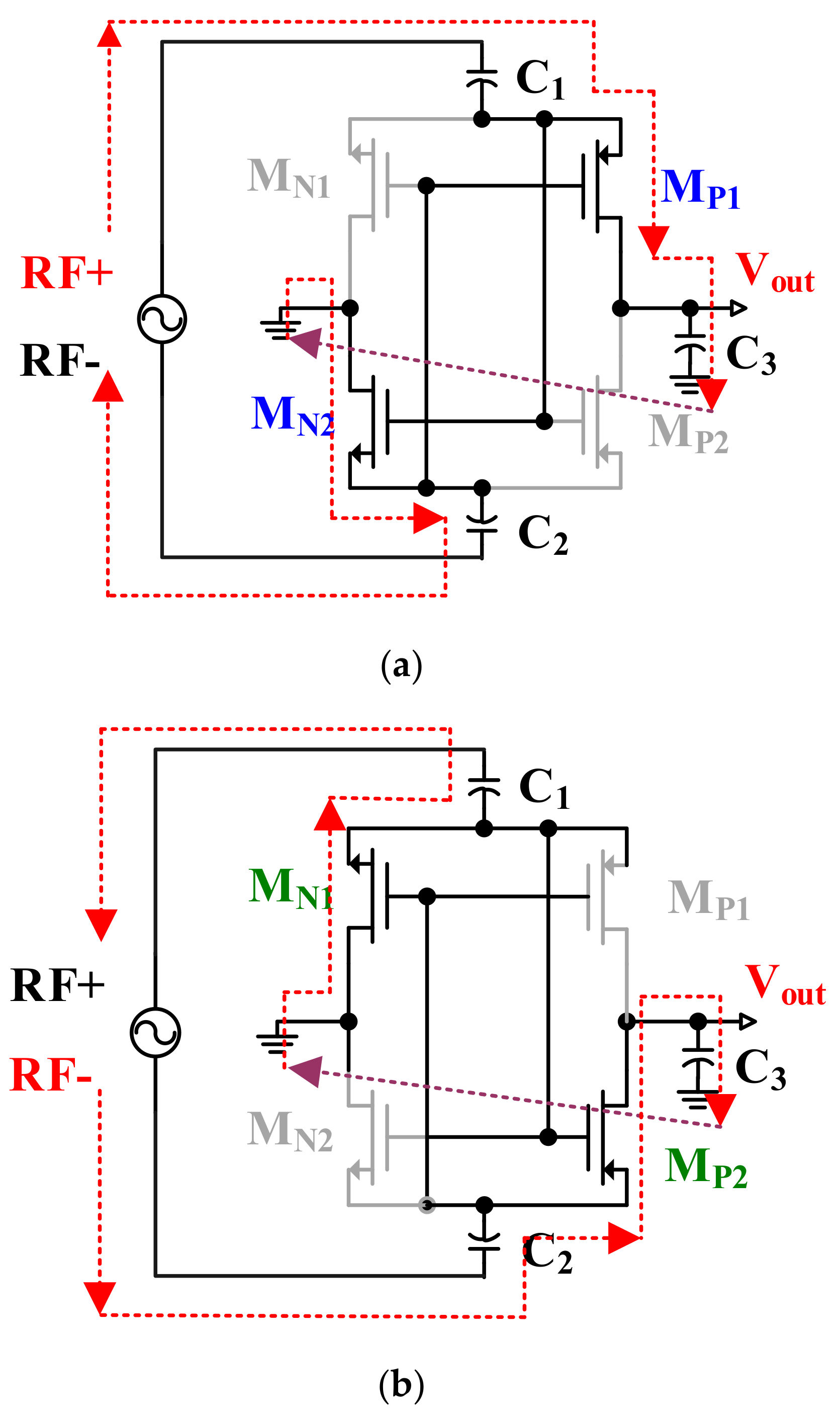
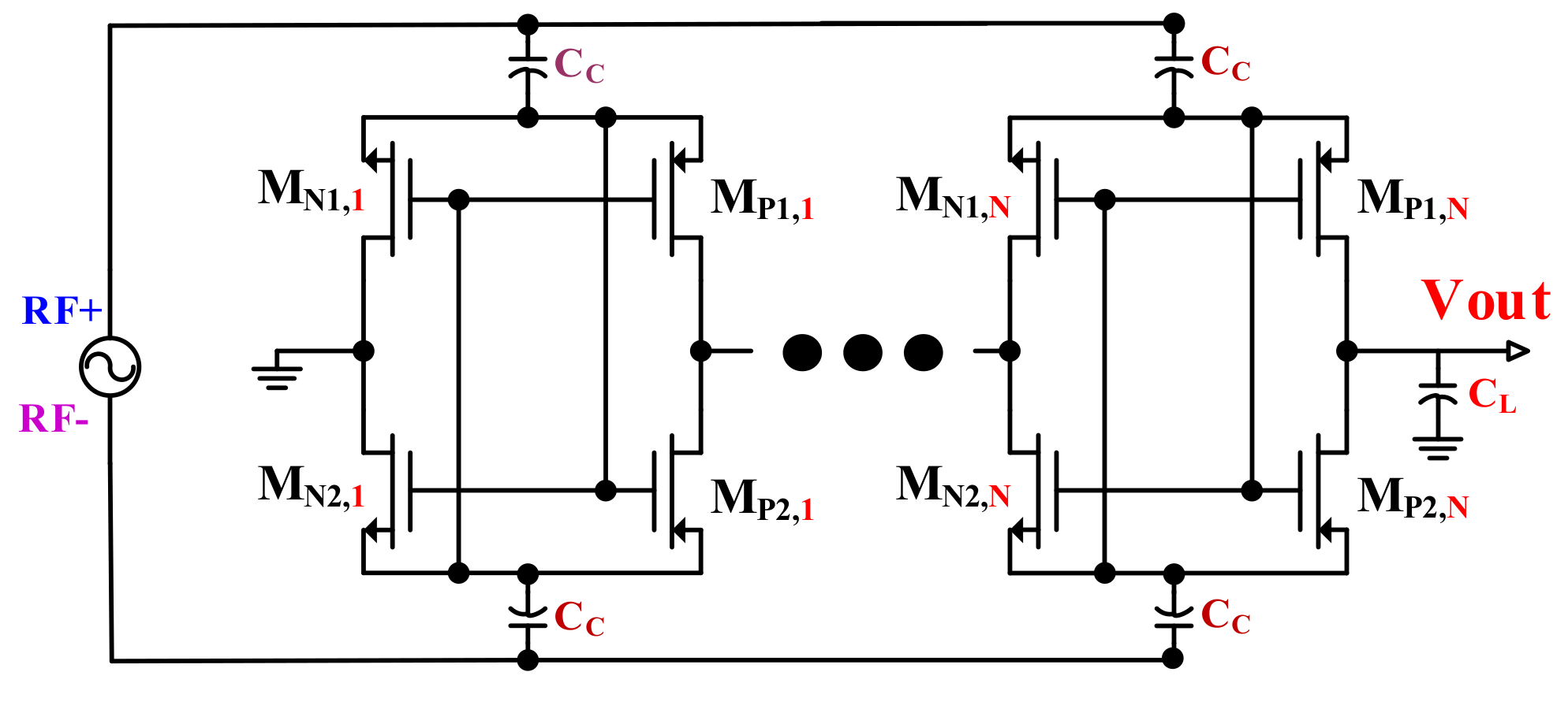
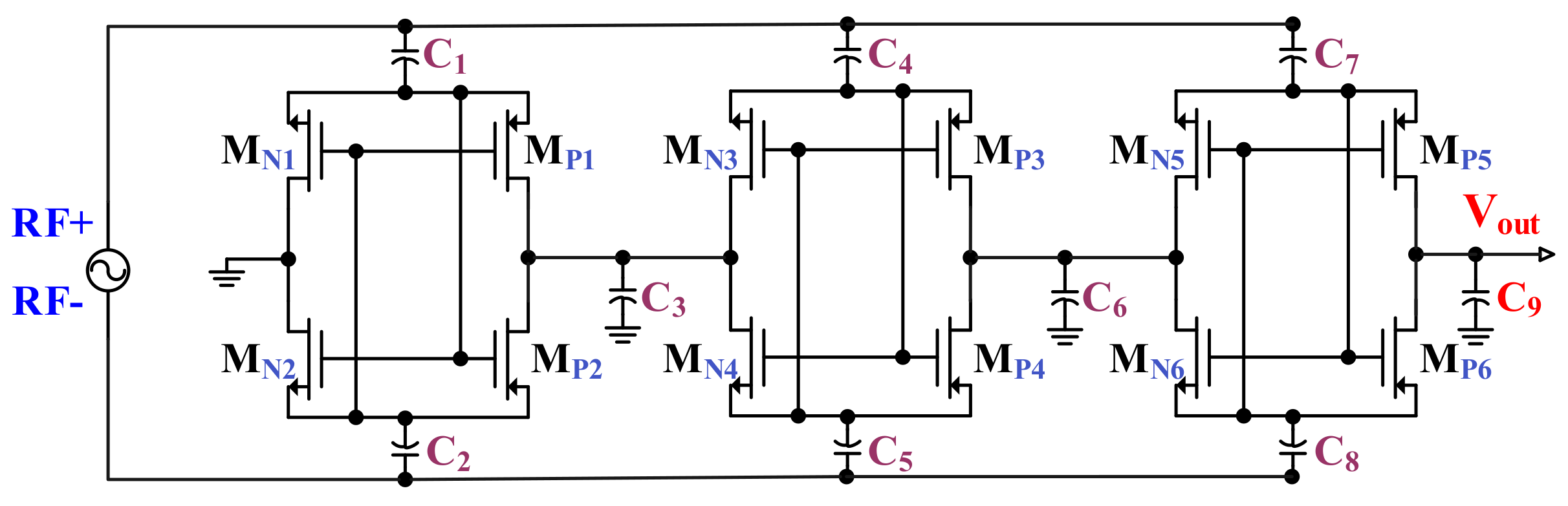
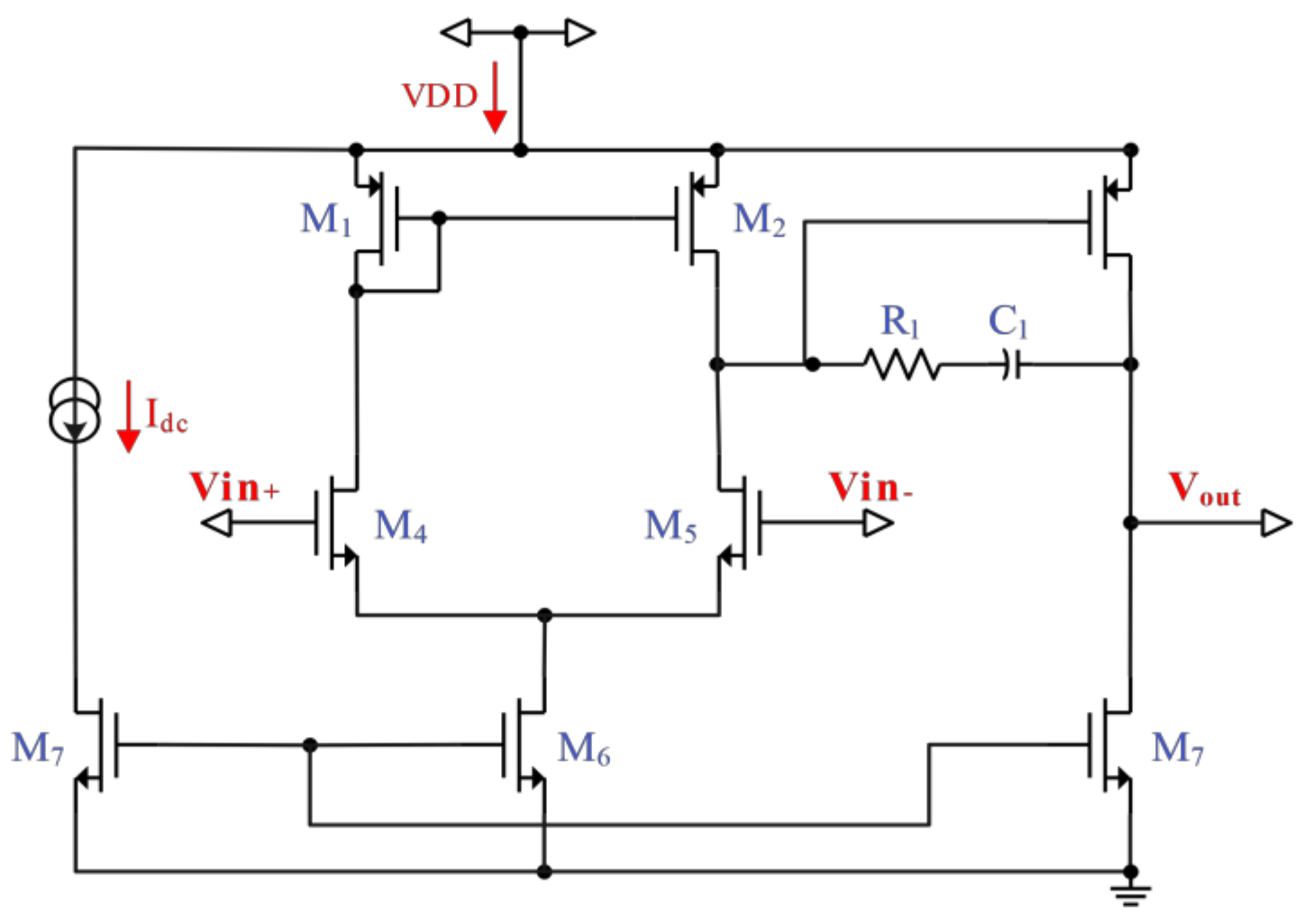
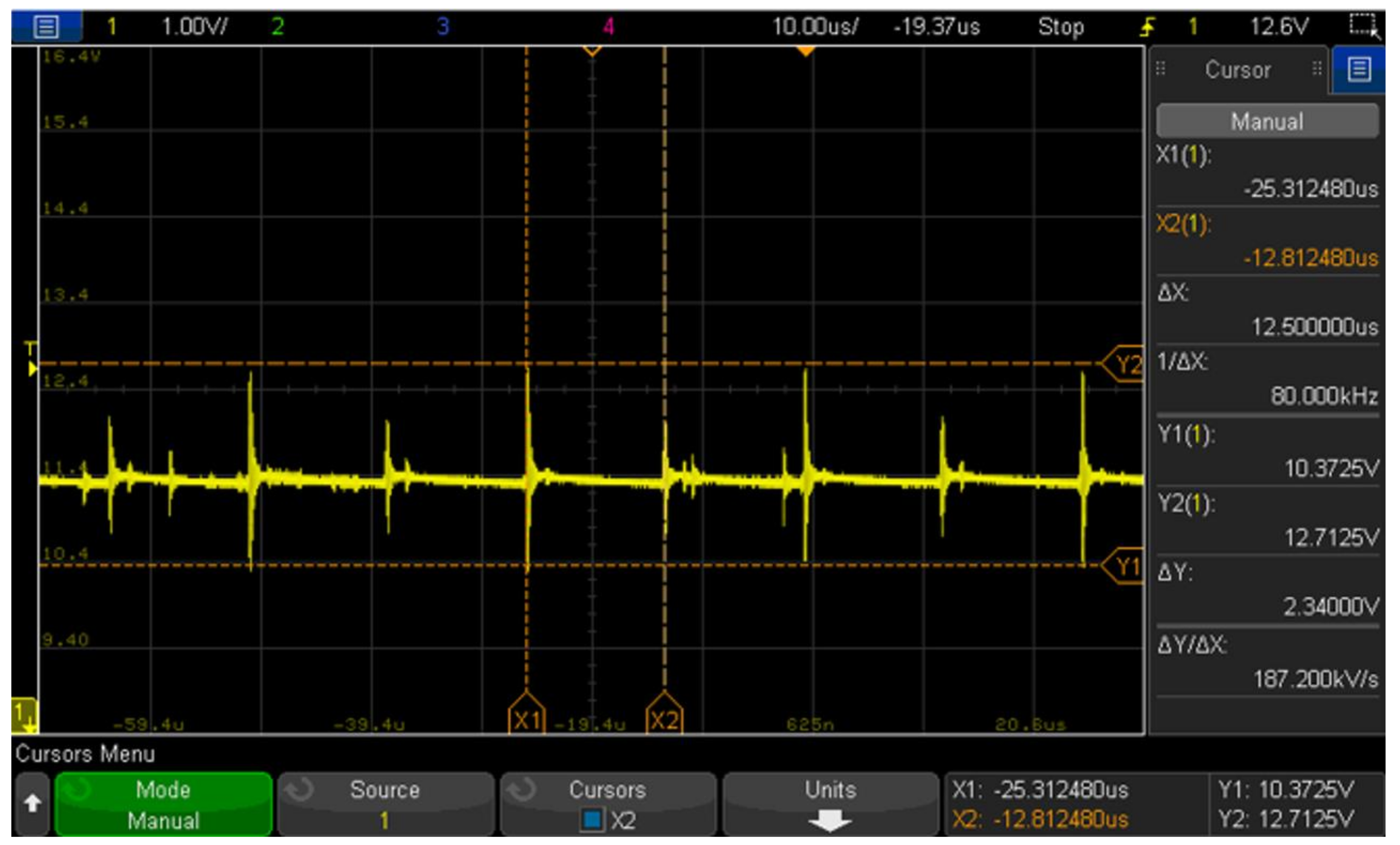
2.3. RF-DC Bridge Rectifier

The “full-wave bridge rectifier” is the most common full-wave rectification circuit that rectifies the desired DC voltage using the input signal’s positive and negative half-cycle signals [18]. In the full-wave bridge rectifier, transistors are connected in a diode manner. During positive half-cycle operation, current flows from Vin+ to the load capacitance CL through the NMOS transistor, whereas during negative half-cycle operation, current flows from Vin− to the load capacitance through the positive-channel metal–oxide–semiconductor (PMOS) transistor. Therefore, the DC voltage can be effectively rectified regardless of whether the rectifier circuit operates in a positive or negative half-cycle. The output voltage can be expressed as follows:
V o u t = 2 V i n V t h
where Vin represents the peak magnitude of the RF signal, and Vth represents the threshold voltage of the metal–oxide–semiconductor field-effect transistor (MOSFET).
Figure 5 illustrates an external Vth cancellation rectifier circuit whose conversion efficiency has been increased by adding a critical voltage Vb between the gate and drain terminals of the transistor [19]. The output voltage Vout can then be expressed as follows:
V o u t = 2 V i n + V b V t h
If Vb equals Vth, then the output voltage Vout is twice the input voltage Vin. Through careful changes to the critical voltage Vb, the threshold voltage Vth can be cancelled to improve the voltage conversion efficiency. However, introducing an external bias voltage to complete the cancellation of Vth is not ideal. Figure 6 presents a circuit design for the self-cancellation of the threshold voltage Vth [20]. As shown in Equation (8), when the critical bias voltage Vb is equal to the threshold voltage Vth, the output voltage Vout becomes 2 × Vin. The critical bias voltage Vb can be implemented using the storage capacitors C1a or C2a. The voltages stored in C1a and C2a provide the necessary cancellation voltages Vb1 and Vb2, which are used to eliminate the threshold voltages Vth1 and Vth2 of transistors M1 and M2, respectively. The self-cancellation of Vth is achieved with the aid of two off-chip resistors, R1 and R2.
Figure 7 shows a single-stage cross-coupled differential drive (CCDD) rectifier circuit [21], which is composed of the CMOS full-wave bridge rectifier and the circuit for the self-cancellation of Vth. The advantages of the proposed CCDD rectifier (CCDDR) are that the input signal can be utilized effectively in each cycle, and the critical voltage can be reduced. When the RF+ terminal is connected to a high-level signal and the RF− terminal connected to a low-level signal, the transistors MP1 and MN2 conduct electricity not only to provide a charging current from RF+ to RF− but also to increase the output voltage Vout (Figure 8a). Conversely, when RF− is at a high potential and RF+ at a low potential, the transistors MP2 and MN1 conduct electricity to provide a charging path from RF− to RF+, thereby increasing the output voltage Vout. C1 and C2 are used as voltage compensation for the transistor gate, and C3 is a regulated capacitor that supplies a stable voltage to the Vout terminal (Figure 8b).
Figure 9 depicts the equivalent circuit when RF+ is positive for a half-cycle. The peak voltages of the RF+ and RF− signals, the capacitance voltages of C1 and C2, and the required minimum voltages of PMOS and NMOS are represented as +Vp, −VP, +VCP, −VCP, |Vth,p|, and Vth,n, respectively. According to Kirchhoff’s voltage law, the charged voltage of VC3 can be expressed as follows:
V C 3 + = V P V C P V t h , p V C 3 = V P V C P + V t h , n
V C 3 = V C 3 + V C 3 = 2 V P V t h , p + V t h , n
During the conduction process, the MOSFET operates as a switch in the linear region. The on-switching impedances of the PMOSFET (MP1) and NMOSFET (MN2) can be expressed as shown in Equations (11) and (12).
r O N _ M P 1 = 1 μ p C o x W L V g s p V t h , p V d s p
r O N _ M N 2 = 1 μ n C o x W L V g s n V t h , n V d s n
where μp and μn represent carrier mobility of PMOS and NMOS, respectively; Cox represents the parasitic capacitance of the gate oxide; W and L represent gate width and length of MOSFET, respectively; Vgs represents the voltage difference between the gate and the source; Vds represents the voltage difference between the drain and the source; and Vth represents the threshold voltage of the transistor.
Figure 10 depicts a multi-order CCDD rectifier circuit, which is composed of many single-stage CCDD rectifier circuits arranged in cascade topology. The purpose of a multi-order CCDD rectifier circuit is to provide the load with enough voltage for the intended application. In general, the output voltage increases with the order of the CCDD rectifier circuit. However, an increase in the order is accompanied by an increase in the number of switch transistors used, resulting in higher losses in the form of leakage voltages. Therefore, the selection of a useful rectifier circuit is based on the system’s conversion efficiency and output voltage. According to Equation (10), the output voltage of the N-order CCDD rectifier circuit can be expressed as follows:
V o u t , N = 2 N V p N V t h , p + V t h , n
This study employs a three-stage CCDD rectifier circuit having six NMOSFETs and six PMOSFETs (in Figure 11) [10]. The circuit contains six nominal N-type transistors and six nominal P-type transistors in the diode-connected form as well as nine metal–insulation–metal capacitors. All transistors and capacitors are identical. The bottom plate, marked with a bold line, exhibits a large parasitic capacitance and is grounded to reduce loss. If the RF signal is received through the ISM-0.915-GHz antenna, it is fed into the CCDD rectifier through the balun and impedance matching network. The load capacitor C9 of the third CCDD rectifier stores enough DC voltage to complete signal conversion and suppress ripple voltage [22].

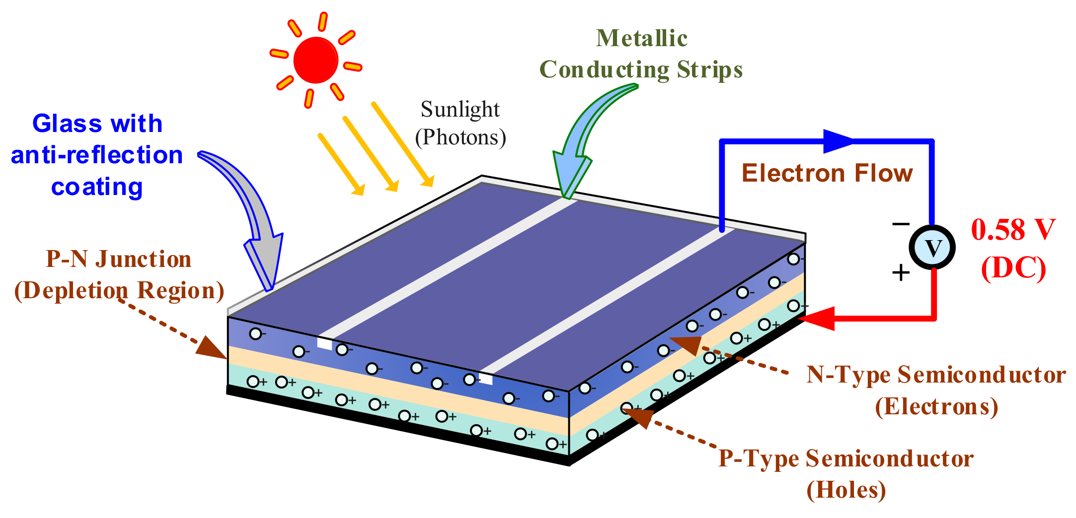
2.4. Solar Energy (PV Cell)

A photovoltaic cell, commonly called a solar cell, is a semiconductor device that converts sunlight directly into electricity. Figure 12 illustrates a photovoltaic cell composed of two semiconductor layers: an N-type layer with an abundance of electrons and a P-type layer with an abundance of holes. Incoming photons strike the photovoltaic cell and are absorbed, resulting in the excitation of electrons in the N-type layer and their migration across the junction to the P-type layer. The movement of electrons toward the front surface of the photovoltaic cell creates an imbalance of electrical charge between the front and back surfaces of the cell, resembling the negative and positive terminals of a battery and creating a voltage potential. Electrical conductors on the photovoltaic cell absorb the electrons. When these conductors are connected in an electrical circuit to an external load, such as a battery, electricity flows through the circuit [23]. Figure 13 shows the most popular equivalent circuit of a solar photovoltaic cell. It includes a current source IPH, one diode with voltage VD and current ID, and two resistors: one in series (RSE) and one in parallel (RP) [24]. Multiple photovoltaic cells can be connected in parallel or in series to increase the output power and voltage. Solar panels differ in terms of their manufacturing technology and the corresponding efficiencies. The conversion efficiency of the solar panels available in the market ranges from 16% to 23%. This study used the poly-passivated emitter (Poly PERC, Shajing, Shenzhen, China) and rear contact solar panel, which has a lower conversion efficiency than the N-type-integrated back contact panel.

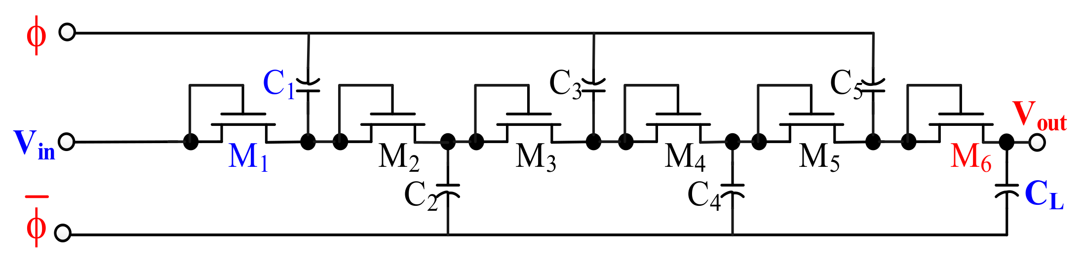
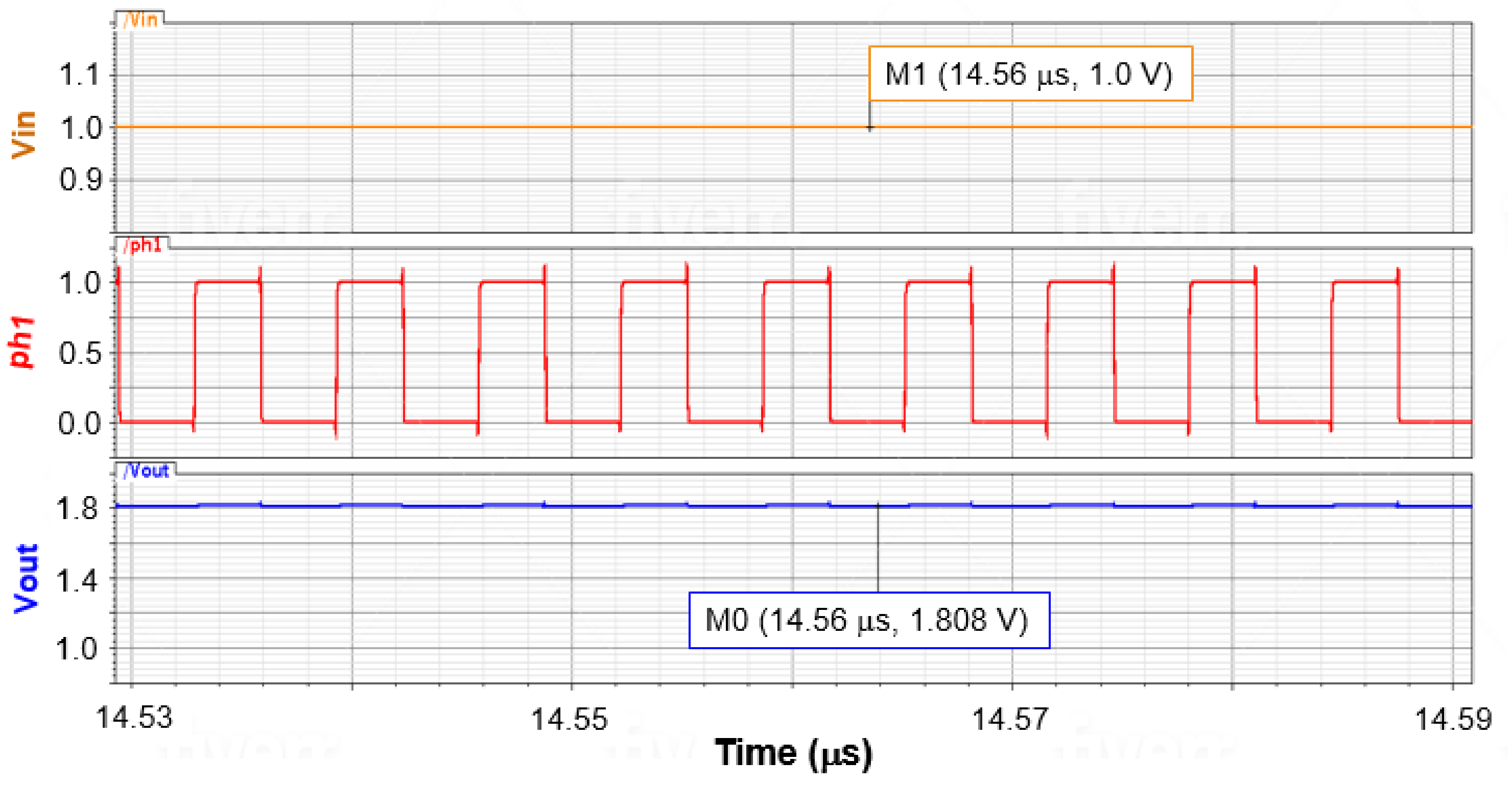
2.5. Dickson Charge Pump

Figure 14 displays a schematic of the Dickson charge pump employed in this study. This pump not only enhances the input power of the solar cell but also generates the required output voltage through multiplication. The N-type MOSFET is configured in a diode-connected form. During the charging phase, the input voltage Vin is supplied to the first stage of the charge pump to charge the first capacitor C1. In the transfer phase, C1 retains its voltage, and the second capacitor C2 gets charged. In the next cycle, the charging process is repeated, and the stored voltage is increased. Finally, the output voltage Vout is obtained from the last load capacitor CL [22].

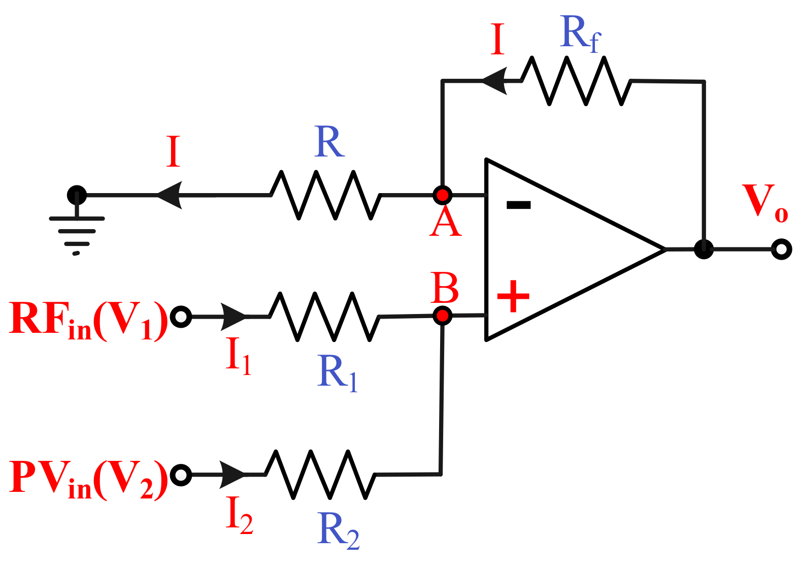
2.6. DC Voltage Combiner

Figure 15 displays a schematic of a DC voltage combiner circuit, which includes two energy sources: RF energy (RFin) and solar energy (PVin). The combination of the two voltages is achieved through the use of a noninverting summing amplifier, which comprises an operational amplifier with two input resistors, R1 and R2, connected to its noninverting input terminal (+). The inverting input terminal (−) is typically connected to the ground or a reference voltage (Vref). The two input resistors, R1 and R2, are connected to two input voltage sources, V1 and V2, respectively. The noninverting input terminal draws negligible current because it is connected to a high-input impedance, resulting in virtual grounding at the noninverting and inverting terminals (i.e., VA = VB). The output voltage (Vo) is the sum of the weighted input voltages, determined by the ratio of the feedback resistance (Rf) to the respective input resistances (R1 or R2). Based on these weighting factors, the summing amplifier combines the input voltage sources, RFin (V1) and PVin (V2), to produce a summed output voltage [25].
V o = 1 + R f R × R 2 R 1 + R 2 V 1 + R 1 R 1 + R 2 V 2
where V1 represents an RF energy source (RFin) and V2 represents a solar energy source (PVin). Figure 16 presents a circuit diagram of the adopted two-stage operational amplifier with compensation. The CC is chosen large enough to position the dominant pole properly, and the RZ moves the right half plane to zero [26].

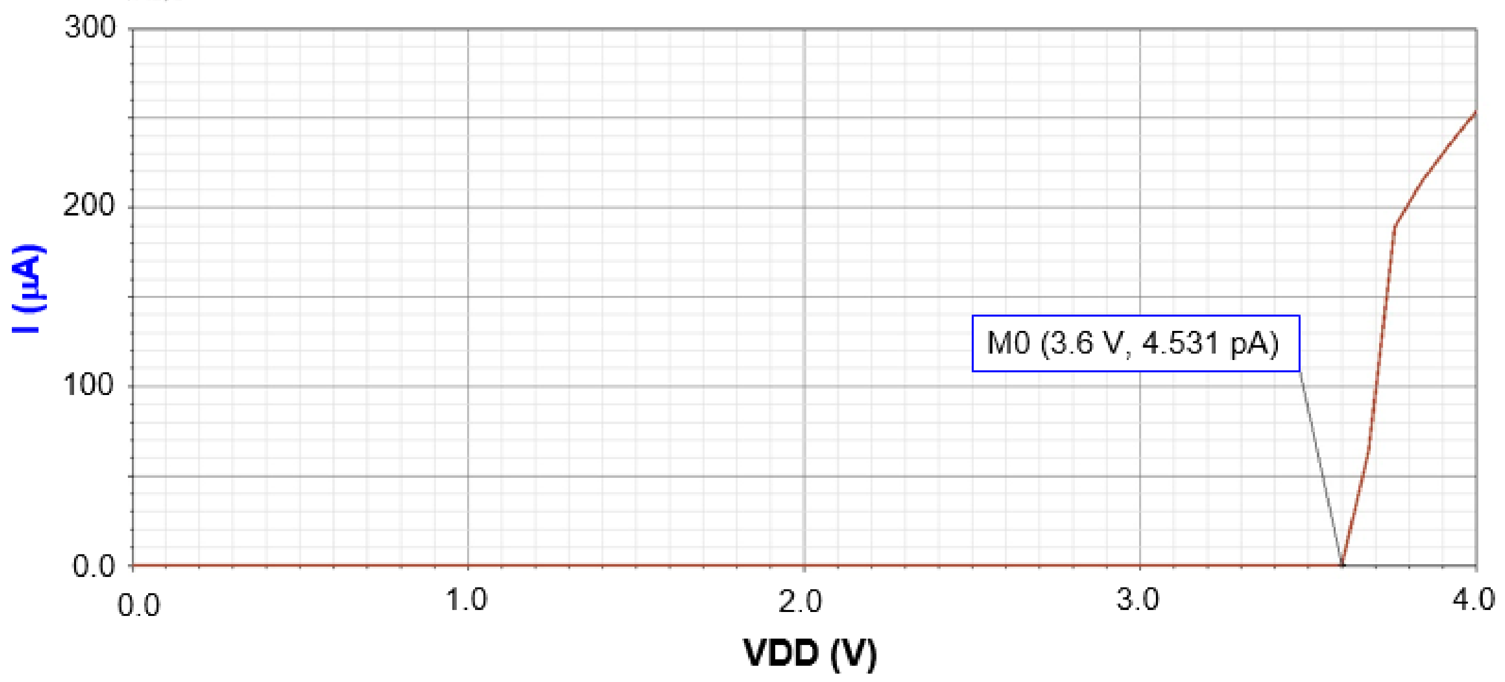
2.7. Overvoltage Protection (OVP) Circuit

The OVP circuit is a critical component of the RF- and solar-energy-harvesting system. When the output voltage of the RF–DC or DC–DC converter is too high in the near-field energy region, the OVP circuit helps prevent the breaking or burning of the harvesting chip. Figure 17 shows a schematic of an OVP circuit [17]; the diode-connected form of the transistor M7 is utilized to fix the voltage VB, and the voltage VA is decided using the division between the two transistors M1 and M2. An increase in the output voltage Vdc will create a voltage difference between VA and VB, elevating the amplifier output voltage. Consequently, the MO transistor switches on and conducts the current to the ground, further stabilizing VA until VA = VB. The MO current is fixed to stabilize the rectifier output voltage Vdc. The differential output voltage VO is used to control the conduction current IO of the output transistor MO. The larger the DC voltage Vdc, the larger the conduction current IO. Thus, a stable DC output voltage is generated. The two bias voltages VA and VB could be expressed as follows:
V A = V d c V O D 1 + V t h , p 1 V O D 2 + V t h , p 2
V B = V O D 7 + V t h , n 7
where VODi, Vth,ni, and Vth,pi represent the overdrive voltage of the ith MOSFET, threshold voltage of the ith NMOS, and the threshold voltage of the ith PMOS, respectively. Initially, the two bias voltages were identical (i.e., VA = VB). The DC output voltage of the DC voltage combiner can be expressed as follows:
V d c = V g s p 1 + V g s p 2 + V g s n 7
where Vgspi and Vgsni represent the gate-source voltages of the ith diode-connected PMOS and NMOS, respectively.

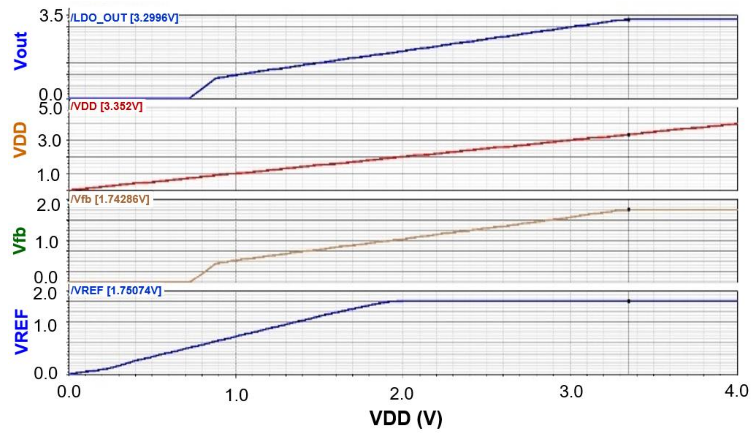
2.8. Low-Dropout Linear Voltage Regulator

In hybrid energy-harvesting systems, a stable and clean output voltage with minimal power loss and low energy consumption is crucial, and the low-dropout regulator (LDO) plays a vital role in achieving this objective. An LDO circuit is proposed in [14], which consists of a CMOS reference voltage, a current source, an error amplifier, a feedback network, frequency compensation, and a load. The operating principle of the LDO circuit is as follows: the positive terminal (+) of the error amplifier is connected to a precise CMOS reference voltage (VREF), while the negative terminal (−) is connected to the feedback voltage (VFB) from the output. By comparing VREF and VFB, the error amplifier generates an amplified error signal to adjust the gate voltage of the pass transistor. When the feedback voltage exceeds the reference voltage, the error amplifier produces a higher gate voltage, which reduces the output current of the pass transistor. As a result, the output voltage decreases along with the output current through the load, which includes equivalent resistors [27].

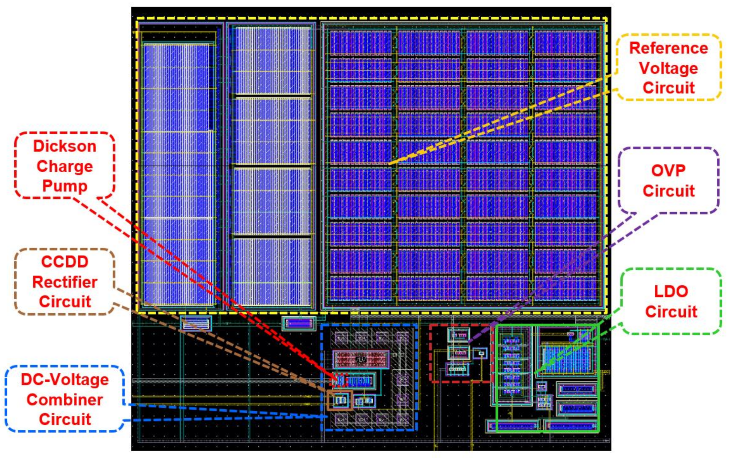
3. Simulation Results

The solar energy system operates at high voltage, and its leakage current may damage the proposed RF harvesting chip. This poses a challenge to integrating both systems into a single chip. As a result, this study is presented as a simulation-based work. Experimental measurements are not included due to these integration challenges. Further efforts are needed to mitigate these issues, particularly through the development of appropriate protection circuitry. Figure 18 shows the DC and AC leakage voltages of the solar energy harvesting system. It can be observed that the leakage voltages ranges from 10.3725 V to 12.7125 V. These leakage voltages damage the RF chip, as its maximum supply voltage is approximately 1.8 V under the 0.18 μm CMOS process. Future work will focus on designing a protection circuit between the RF chip and the solar chip.
As shown in Figure 4, a matching network of (28.71 − j × 154.2) Ω is added to the system to guarantee that the input impedance Zin of the rectifier is approximately 50 Ω. The matching network was simulated using ADS software. Figure 19 illustrates the parameter S11 of the matching network. The input return loss S11 at the center frequency of 0.915 GHz is approximately −30.161 dB, lower than −25 dB. The simulated input return loss satisfies the required specification.
As shown in Figure 11, the RF input signal is received through the ISM–0.915–GHz antenna and fed into the three–stage CCDD rectifier through the balun and matching network. Let us regard the input RF signal as a cosine waveform (i.e., RFin = VP cosωt, with a peak amplitude VP and an input frequency f = ω/2π = 1/T). The load capacitor C9 stores enough voltage to complete the signal conversion and suppress the ripple voltage. When the rectifier circuit operates in a positive half–cycle (t = 0, T, 2T, …), the transistors MP1, MN2, MP3, MN4, MP5, and MN6 conduct electricity, and the forward current flows into C3, C6, and C9. The DC output voltage Vout is obtained at C9. When the rectifier circuit operates in a negative half–cycle (t = T/2, 3T/2, …), the transistors MN1, MP2, MN3, MP4, MN5, and MP6 conduct electricity, and a backward current flows into C3, C6, and C9. An output voltage Vout is obtained at C9. The conversion efficiency of the differential three-stage CCDD rectifier circuit is twice that of a single-ended rectifier circuit. All transistors and capacitors continue to operate as described above regardless of the number of stages of the voltage doubler and rectifier. If the number of stages is three, the approximate output voltage is calculated as follows: Vout = 6 × VP − 3 × (|Vth,p| + Vth,n) (V). Figure 20 shows the simulated conversion efficiency of the adopted differential three-stage CCDD rectifier circuit. The maximum conversion efficiency was approximately 41.68% at an input RF power of −5.1 dB.
Furthermore, a Dickson charge pump is utilized to boost the input power of the solar cell and to generate the required output voltage through multiplication. Figure 21 presents the simulation results of operating a Dickson charge pump. When the input voltage is approximately 1.0 V, the output voltage is approximately 1.8 V at a phase frequency of 150 MHz. Next, a DC voltage combiner is used to merge the outputs of the two sources, namely, RF energy and solar energy. The output voltage (Vo), given by the sum of the weighted input voltages, is determined from Equation (14). Figure 22 shows the simulation results of operating a summing amplifier. If the output voltages of both RF and solar power are 1.8 V each, they can be combined using the summing amplifier to yield a combined output voltage Vo of approximately 3.552 V at identical resistances (Rf = R and R1 = R2).
Figure 23 illustrates the simulation results of an OVP circuit. A higher input RF or solar voltage corresponds to a larger voltage output by the DC voltage combiner. Once the output voltage reaches the rated voltage of 3.6 V, the excess voltage is dissipated by the proposed OVP circuit. The conductional current Io of the output transistor Mo surges sharply to stabilize the output voltage of 3.6 V.
Finally, an LDO is employed to obtain a stable and clean output voltage with low power loss and low power consumption. Figure 24 shows the simulated output voltage of an LDO. In this simulation, the reference voltage VREF is approximately 1.75074 V, and the feedback voltage VFB is approximately 1.74286 V. The LDO circuit generates a steady output voltage of approximately 3.2996 V.
After the designed functions were verified, the custom design was fabricated on a chip. Figure 25 presents the completed layout of the proposed hybrid RF- and solar-energy-harvesting chip, composed of the CCDD rectifier, Dickson charge pump, DC voltage combiner, OVP circuit, LDO circuit, and reference voltage circuit. The chip area is approximately 0.225 × 0.225 mm2.
Table 1 summarizes the evaluation results of the proposed HEHS compared with other RF–DC rectifiers and hybrid energy-harvesting integrated circuits. The chip area, measuring 0.050625 mm2, is the smallest among all the previously reported designs selected for comparison [28,29,30,31,32]. The input power range (dBm) achieved in this study is also superior to that of the selected designs, and the maximum power conversion efficiency (PCE) obtained is comparable to those reported in previous studies [30,32]. Moreover, the output voltages of the RF, solar, and hybrid energy harvesters reported in this study exceed those of all the selected references. Although several RF–DC rectifiers have been studied in recent years, research on system integration, such as RF energy-harvesting integrated circuits (ICs), remains limited. The proposed hybrid energy-harvesting IC features low power consumption and a compact chip area. Labor costs can be significantly reduced by eliminating the need for future battery replacements. At close range, the proposed IC can be used to trickle-charge low-power devices such as GPS modules, tracking tags, wearable sensors, and consumer electronics. At longer ranges, the transmitted power can support battery-based or battery-free remote sensors for factory automation, structural health monitoring, and industrial control. It is worth noting that a recent trend in hybrid energy-harvesting systems focuses on the integration of photovoltaic (PV) cells, RF energy, and thermoelectric generators (TEGs), which can be fabricated using a 65 nm process [30,31,32]. The peak PCEs of the aforementioned hybrid energy-harvesting chips are comparable to those in this study: 76.1% using a DC adder, 69.0% with a power combiner, and 78% with a DC voltage combiner. These systems can convert otherwise wasted power into additional electrical energy using the cross-coupled charge pump (CCCP) operation, thereby enhancing conversion efficiency or supplementing the main power source to extend service life. In future work, the power conversion efficiency of the hybrid energy-harvesting chip could be further improved by reducing the power consumption of each proposed circuit and integrating it with various power sources.

4. Conclusions

This study presents a hybrid energy-harvesting chip that combines an ISM-0.915-GHz RF energy acquisition system with a solar photovoltaic cell. A CCDD rectifier is employed to convert the RF signal into DC voltage. The input solar voltage is then boosted from 1.0 to 1.8 V using a Dickson charge pump. A DC voltage combiner is used to combine the RF energy with solar energy. An OVP circuit is connected at the rectifier’s output to protect the LDO and to limit the output voltage to within 3.6 V. Finally, an LDO is utilized to ensure a stable output voltage of 3.2996 V. The simulation results indicate that the RF rectifier circuit achieves a maximum power conversion efficiency of 41.6% and a steady output voltage of 3.2996 V. This study demonstrates the effectiveness of the proposed HEHS in efficiently harvesting and managing RF and solar energies. Its potential applications include charging low-power devices such as IoT devices, wearable electronics, and biomedical systems [33]. Future work will focus on integrating the RF energy-harvesting system with advanced conversion techniques, including maximum power point tracking (MPPT), dipole antenna arrays, rectenna arrays, and harmonic-based applications.

Author Contributions

Conceptualization, G.-M.S., S.-H.C., V.C., and C.-P.Y.; methodology, G.-M.S., S.-H.C., and V.C.; validation, S.-H.C. and V.C.; formal analysis, G.-M.S., S.-H.C., and V.C.; investigation, G.-M.S., S.-H.C., and V.C.; writing—original draft preparation, S.-H.C. and V.C.; writing—review and editing, G.-M.S. and C.-P.Y.; supervision, G.-M.S. and C.-P.Y.; project administration, G.-M.S. and C.-P.Y.; funding acquisition, G.-M.S. All authors have read and agreed to the published version of the manuscript.

Funding

This research was funded by the National Science and Technology Council (NSTC), Taiwan, under grant number NSTC 113-2622-E-027-001.

Data Availability Statement

The data presented in this study are available in this article.

Acknowledgments

The authors wish to thank the National Science and Technology Council, Taiwan, for financially supporting this research under Contract No. NSTC 113-2622-E-027-001. They also extend their gratitude to the Taiwan Semiconductor Research Institute (TSRI) for fabricating the test chip.

Conflicts of Interest

The authors declare no conflicts of interest.

References

  1. Shafique, M.T.; Kamran, H.; Arshad, H.; Khattak, H.A. Home energy monitoring system using wireless sensor network. In Proceedings of the 14th International Conference Emerging Technologies (ICET), Islamabad, Pakistan, 21–22 November 2018; pp. 1–6. [Google Scholar]
  2. Xu, P.; Flandre, D.; Bol, D. Analysis, modeling, and design of a 2.45-GHz RF energy harvester for SWIPT IoT smart sensors. IEEE J. Solid-State Circuits 2019, 54, 2717–2729. [Google Scholar] [CrossRef]
  3. Chen, P.Y.; Chen, B.Y.; Chang, C.H.; Cheng, J.Y.; Chen, S.S.; Yang, M.M.; Hu, W.W. An RF-DC converter IC for power charging application. In Proceedings of the International Conference Engineering Technologies and Applications (IET-ICETA), Changhua, Taiwan, 14–16 October 2022; pp. 1–2. [Google Scholar]
  4. Sung, G.M.; Chou, H.Y.; Chen, Z.W. Radio frequency energy harvesting IC for ISM-915 MHz and 2.45 GHz wireless transmitter. In Proceedings of the IEEE International Future Energy Electronics Conference (IFEEC), Taipei, Taiwan, 16–19 November 2021; pp. 1–5. [Google Scholar]
  5. Lin, S.H.; Kuo, C.Y.; Lu, S.Y.; Liao, Y.T. A high-efficiency power management IC with power-aware multi-path rectifier for wide-range RF energy harvesting. In Proceedings of the IEEE MTT-S International Microwave Symposium (IMS), Honololu, HI, USA, 4–9 June 2017; pp. 303–306. [Google Scholar]
  6. Seong, D.; Jang, K.; Hwang, W.; Jeon, H.; Choi, J. Radio-frequency energy-harvesting IC with DC-DC converter. In Proceedings of the International SoC Design Conference (ISOCC), Jeju, Republic of Korea, 23–26 October 2016; pp. 339–340. [Google Scholar]
  7. Adami, S.E.; Vollaire, C.; Allard, B.; Costa, F.; Haboubi, W.; Cirio, L. Ultra-low power autonomous power management system with effective impedance matching for RF energy harvesting. In Proceedings of the 8th International Conference on Integrated Power Electronics Systems, Nuremberg, Germany, 25–27 February 2014; pp. 1–6. [Google Scholar]
  8. Chang, C.L.; Lee, T.C. An thermoelectric and RF multi-source energy harvesting system. In Proceedings of the 2nd International Conference on Intelligent Green Building and Smart Grid, Prague, Czech Republic, 27–29 June 2016; pp. 1–5. [Google Scholar]
  9. Saini, G.; Somappa, L.; Baghini, M.S. A 500-nW-to-1-mW input power inductive boost converter with MPPT for RF energy harvesting system. IEEE J. Emerg. Sel. Top. Power Electron. 2021, 9, 5261–5271. [Google Scholar] [CrossRef]
  10. Atsushi, S.; Koji, K.; Takashi, I. Differential-drive CMOS rectifier for UHF RFIDs with 66% PCE at −12 dBm input. In Proceedings of the IEEE Asian Solid-State Circuits Conference (ASSCC), Fukuoka, Japan, 3–5 November 2008; pp. 105–108. [Google Scholar]
  11. Hamza, M.; Rehman, M.U.; Riaz, A.; Maqsood, Z.; Khan, W.T. Hybrid dual band radio frequency and solar energy harvesting system for making battery-less sensing nodes. In Proceedings of the IEEE Radio and Wireless Symposium (RWS), San Diego, CA, USA, 17–22 January 2021; pp. 116–118. [Google Scholar]
  12. Jadhav, S.B.; Lambor, S.M. Hybrid solar and radio frequency (RF) energy harvesting. In Proceedings of the IEEE International Conference Power, Control, Signals and Instrumentation Engineering (ICPCSI), Chennai, India, 21–22 September 2017; pp. 1975–1980. [Google Scholar]
  13. Farooq, A.; Gray, M.; Bao, X.; Wu, X. Hybrid RF-solar energy harvesting for IoT. In Proceedings of the 34th Irish Signals and Systems Conference (ISSC), Dublin, Ireland, 13–14 June 2023; pp. 1–5. [Google Scholar]
  14. Yu, B.Y.; Wang, Z.H.; Ju, L.; Zhang, C.; Liu, Z.G.; Tao, L.; Lu, W.B. Flexible and wearable hybrid RF and solar energy harvesting system. IEEE Trans. Antennas Propag. 2022, 70, 2223–2233. [Google Scholar] [CrossRef]
  15. Shi, Y.; Nan, Y.H. Hybrid power harvesting from ambient radiofrequency and solar energy. IEEE Antennas Wirel. Propag. Lett. 2022, 21, 2382–2386. [Google Scholar] [CrossRef]
  16. Williams, J.M.; Gao, F.; Qian, Y.; Song, C.; Khanna, R.; Liu, H. Solar and RF energy harvesting design model for sustainable wireless sensor tags. In Proceedings of the IEEE Topical Conference Wireless Sensors and Sensor Networks (WiSNeT), San Antonio, TX, USA, 26–29 January 2020; pp. 1–4. [Google Scholar]
  17. Sung, G.M.; Chung, C.K.; Lai, Y.J.; Syu, J.Y. Small-area radiofrequency energy harvesting integrated circuits for powering wireless sensor networks. Sensors 2019, 19, 1754. [Google Scholar] [CrossRef] [PubMed]
  18. Hashemi, S.; Sawan, M.; Savaria, Y. A novel low-drop CMOS active rectifier for RF-powered devices: Experimental result. Microelectron. J. 2009, 40, 1547–1554. [Google Scholar] [CrossRef]
  19. Umeda, T.; Yoshida, H.; Sekine, S.; Fujita, Y.; Suzuki, T.; Otaka, S. A 950-MHz rectifier circuit for sensor network tags with 10-m distance. IEEE J. Solid-State Circuit 2006, 41, 35–41. [Google Scholar] [CrossRef]
  20. Nakamoto, H.; Yamazaki, D.; Yamanmoto, T.; Kurata, H.; Yamada, S.; Miksida, K.; Ninomiya, T.; Ohkawa, T.; Masui, S.; Gotoh, K. A passive RFID RF identification CMOS tag IC using ferroelectric RAM in 0.35-μm technology. IEEE J. Solid-State Circuit 2007, 42, 101–110. [Google Scholar] [CrossRef]
  21. Koji, K.; Ito, T. High-efficiency CMOS rectifier circuit with self-Vth-cancellation and power regulator functions for UHF RFIDs. In Proceedings of the IEEE Asian Solid-State Circuits Conference, Jeju, Republic of Korea, 12–14 November 2007; pp. 119–122. [Google Scholar]
  22. Yi, J.; Ki, W.H.; Tsui, C.Y. Analysis and design strategy of UHF micro-power CMOS rectifiers for micro-sensor and RFID applications. IEEE Trans. Circuits Syst. I Regul. Pap. 2007, 54, 153–166. [Google Scholar] [CrossRef]
  23. Boyle, G. Renewable Energy: Power for a Sustainable Future, 2nd ed.; Oxford University Press: Oxford, UK, 2004. [Google Scholar]
  24. Javier, C.; Pindado, S.; Manuel, C.D. Explicit expressions for solar panel equivalent circuit parameters based on analytical formulation and the Lambert W-function. Energies 2014, 7, 4098–4115. [Google Scholar] [CrossRef]
  25. Ambrosio, R.; Alba, R.T.; Guerrero-C, J.F.; Gonzalez, V.; Limon, A.; Moreno, M. Energy harvesting combining three different sources for low power applications. In Proceedings of the International Conference on Electrical Engineering, Computing Science and Automatic Control (CCE), Mexico City, Mexico, 28–30 October 2015; pp. 1–6. [Google Scholar]
  26. Johns, D.; Martin, K. Analog Integrated Circuit Design; John Wiley & Sons, Inc.: New York, NY, USA, 1997. [Google Scholar]
  27. Sun, M.; Ranasinghe, D.; Said, F.; Al-Sarawi, S.F. RF energy harvester with peak power conversion efficiency tracking. In Proceedings of the IEEE Asia Pacific Conference on Circuits and Systems (APCCAS), Jeju, Republic of Korea, 25–28 October 2016; pp. 107–110. [Google Scholar]
  28. Lai, W.C.; Jang, S.L.; Huang, C.Y.; Juang, M.H. Fully-integrated CMOS DC-DC boost converter. In Proceedings of the IEEE Asia Power and Energy Engineering Conference (APEEC), Chengdu, China, 29–31 March 2019; pp. 84–88. [Google Scholar]
  29. Chong, G.; Ramiah, H.; Yin, J.; Rajendran, L.; Wong, W.R.; Mark, P.I.; Martins, R.P. CMOS cross-coupled differential-drive rectifier in subthreshold operation for ambient RF energy harvesting-model and analysis. IEEE Trans. Circuits Syst. II Express Briefs 2019, 66, 1942–1946. [Google Scholar] [CrossRef]
  30. Hegde, C.; Moham, A.; Mondal, S.; Paily, R.P. A wide dynamic range differential drive CMOS rectifier for μwatts RF energy harvesting systems. In Proceedings of the 38th International Conference on VLSI Design and 23rd International Conference on Embedded Systems (VLSID), Bangalore, India, 4–8 January 2025; pp. 175–179. [Google Scholar]
  31. Diangco, M.M.C.; Gerasta, O.J.L. Multiple-input energy harvesting DC adder combiner for Internet of Things (IoT) wireless sensor nodes (WSN) applications in 65nm CMOS technology. In Proceedings of the IEEE 11th International Conference on Humanoid, Nanotechnology, Information Technology, Communication and Control, Environment, and Management (HNICEM), Laoag, Philippines, 29 November–1 December 2019; pp. 1–6. [Google Scholar]
  32. Acut, R.V.P.; Hora, J.A.; Gerasta, O.J.L.; Zhu, X.; Dutkiewicz, E. PV-TEG-WiFi multiple sources design energy harvesting system for WSN application. In Proceedings of the IEEE International Circuits and Systems Symposium (ICSyS), Kuantan, Malaysia, 18–19 September 2019; pp. 1–5. [Google Scholar]
  33. Laganà, F.; Bibbò, L.; Calcagno, S.; Carlo, D.D.; Pullano, S.A.; Pratticò, D.; Angiulli, G. Smart electronic device-based monitoring of SAR and temperature variations in indoor human tissue interaction. Appl. Sci. 2025, 15, 2439. [Google Scholar] [CrossRef]
Figure 1. Block diagram of the hybrid energy-harvesting system.
Electronics 14 02192 g001
Figure 2. Balun in the hybrid energy-harvesting system.
Electronics 14 02192 g002
Figure 3. Ideal impedance conversion component.
Electronics 14 02192 g003
Figure 4. Matching network configured between the antenna and the NMOS rectifier.
Electronics 14 02192 g004
Figure 5. Rectifier circuit for external cancellation of the threshold voltage (Vth).
Electronics 14 02192 g005
Figure 6. Rectifier circuit for self-cancellation of the threshold voltage (Vth).
Electronics 14 02192 g006
Figure 7. Single-stage cross-coupled differential drive rectifier circuit.
Electronics 14 02192 g007
Figure 8. Charging paths of rectifier circuit. (a) Charging from RF+ to RF– during the positive half-cycle, (b) Charging from RF- to RF+ during the negative half-cycle.
Electronics 14 02192 g008
Figure 9. Equivalent circuit during the positive half-cycle.
Electronics 14 02192 g009
Figure 10. Multi-order CCDD rectifier circuit.
Electronics 14 02192 g010
Figure 11. Three-stage CCDD rectifier circuit, including six NMOSFETs and six PMOSFETs.
Electronics 14 02192 g011
Figure 12. Photovoltaic cell composed of two semiconductor layers: an N-type layer with an abundance of electrons and a P-type layer with an abundance of holes.
Electronics 14 02192 g012
Figure 13. Equivalent circuit of a solar photovoltaic cell.
Electronics 14 02192 g013
Figure 14. Schematic of a Dickson charge pump.
Electronics 14 02192 g014
Figure 15. Noninverting summing amplifier.
Electronics 14 02192 g015
Figure 16. Two-stage operational amplifier with compensation used in the DC voltage combiner.
Electronics 14 02192 g016
Figure 17. Schematic of an overvoltage protection circuit.
Electronics 14 02192 g017
Figure 18. The solar energy harvesting system’s leakage DC and AC voltages vary from 10.3725 V to 12.7125 V with the noises generated from the hair dryer.
Electronics 14 02192 g018
Figure 19. Simulated input return loss S11 of the matching network.
Electronics 14 02192 g019
Figure 20. Simulated conversion efficiency of the differential three-stage CCDD rectifier with respect to the input RF power.
Electronics 14 02192 g020
Figure 21. Simulation results of operating a Dickson charge pump.
Electronics 14 02192 g021
Figure 22. Simulation results of operating a summing amplifier with two input voltages, Vin1 and Vin2, and an output voltage Vout.
Electronics 14 02192 g022
Figure 23. Simulated output voltage is approximately 3.6 V for the proposed overvoltage protection circuit.
Electronics 14 02192 g023
Figure 24. Simulated output voltage is approximately 3.2996 V for the low-dropout linear voltage regulator.
Electronics 14 02192 g024
Figure 25. Layout of the proposed hybrid RF- and solar-energy-harvesting chip.
Electronics 14 02192 g025
Table 1. Summary of performance and its comparison with those of other RF-DC rectifiers, RF energy-harvesting ICs, and hybrid energy-harvesting ICs.
Reference
(Year)
[28]
(2019)
[29]
(2019)
[30]
(2025)
[31]
(2019)
[32]
(2021)
This
Work
Technology180 nm180 nm65 nm65 nm65 nm180 nm
Harvesting sourcesRFRFRFPV + RF + TEGPV + TEG + WiFiRF + Solar
RF frequency (MHz)2300900953-2400915
Input power range (dBm)−20~+15−20~+0−25~0-0.5 V−5~+20
Rectifier topology2-stage
CCR
3-, 4-, and 7-stage
CCDDR
Fully
self-biased
2-stage
CCCP
CCCP3-stage
CCDDR
Peak PCE (rectifier)7.6%42.3%60.5%41.9% (RF)
76.1% (DC Adder)
69.0%
(Combiner)
41.6% (RF)
78% (Solar)
RF output voltage (V)0.6/1.71.31.40.50.921.8
Solar output voltage (V)---0.56.301.8
Hybrid harvester (V)---1.0-3.2996
Chip area (mm2)1.109--0.086-0.050625
RemarksPoorAverageGoodGoodExcellentGood
Disclaimer/Publisher’s Note: The statements, opinions and data contained in all publications are solely those of the individual author(s) and contributor(s) and not of MDPI and/or the editor(s). MDPI and/or the editor(s) disclaim responsibility for any injury to people or property resulting from any ideas, methods, instructions or products referred to in the content.

