Abstract
This paper focuses on the digital closed-loop design for a step-up converter with hybrid switching. For this purpose, for the first time, the control-to-output small-signal transfer function of a hybrid switching converter is determined in the rational form. Based on it, a type 3 analog controller is designed, and then, its digitized counterpart is found, and the digital controller is designed using a digital signal processor. The closed-loop operation is then validated both through simulation and practical implementation.
1. Introduction
Step-up converters are widely used in high-voltage applications such as electrical vehicles, fuel cell applications, photovoltaic systems, uninterruptible power supplies and many more. This type of application benefits from a high step-up gain, which can be obtained using several methods. The literature provides plentiful examples regarding high step-up gain by using either coupled inductors [1], additional voltage multiplier units [2], novel topologies [3], improved switching techniques [4] or isolated converter topologies [5], and many more. Quadratic and cubic converters also provide a much higher gain. Many of the solutions use a single active switch and multiple diodes, requiring fewer components for the driver circuitry. Furthermore, this also makes the control scheme simpler. However, diodes exhibit higher conduction losses compared to transistors, which is one of the main drawbacks of these topologies. The conduction losses can be minimized by using converters which employ fewer diodes. One topology that uses less diodes is the hybrid switching converter proposed by Prof. S. Ćuk in [6] together with the concept of hybrid switching.
The goal of hybrid switching is to achieve a higher efficiency at lower switching frequencies. The hybrid switching converter exhibits two topological states: it operates in a resonant manner during one topological state and as a pulse width modulation (PWM) converter during the other topological state. The hybrid switching converter resembles the PWM converters in the sense that it can be easily duty cycle controlled. Based on the converter presented in [6] and by rotating its switching cell, several step-up, step-down and step-up/step-down hybrid converters can be obtained [7].
In [8], the authors propose a novel low stress step-up converter operating under the hybrid switching principle. The proposed topology, which is one of the topologies obtained by cell rotation as mentioned earlier, has a static conversion ratio higher than the classical boost converter. Compared to the examples presented in the literature, this converter offers additional advantages.
The first main advantage is that the converter obtains the desired high gain by using only three switches, only one of them being a transistor. This converter topology resembles one of the three switch converters proposed by D. Zhou in [9]. The main difference is the presence of a small inductor in series with one of the semiconductor switches and hence resulting in a resonant circuit in one of the topological states. It is known that in the case of the classical step-up converter, the voltage stresses on the semiconductor devices are equal to the output voltage. If this voltage is high, then so are the voltage stresses. Furthermore, the switching and conduction losses will also be high, which will negatively impact the efficiency of the converter. The hybrid step-up converter offers lower voltage stress for the main switch, which represents the second main advantage of this switching technique. The third main advantage is that the frequency of operation is chosen in such a way that the resonant current starts and ends at zero, and hence, one of the diodes operates with zero current switching. However, the authors of [8] only present an open-loop application of the proposed hybrid step-up converter, while in practice, closed-loop operation is always used. The purpose of this paper is to present how to model and the design principles for closed-loop operation of a hybrid switching converter employing digital control.
Digital control has the benefit of flexibility compared to analog control: the control coefficients can be easily changed in the software, compared to changing physical components. However, the main advantage of analog controllers is that they are faster than digital controllers. The limiting factor in digital control is the sampling frequency of the analog to digital converters used for sampling the converter signals (voltages, currents). Considering both possible control approaches, the added flexibility, versatility and ease of implementation are the key factors for choosing a digital controller implementation. There are several examples found in the literature where digital control was employed for dc-dc converters.
Digital controllers can be easily implemented using one of the many development boards built for digital signal processors (DSPs) and field programmable gate arrays (FPGAs), as can be seen in [10,11,12,13,14,15,16,17,18]. A short state-of-the-art review of digital control implementations is presented in the next paragraph. In [10], the authors propose a hardware in the loop (HIL) system that is meant for both developing and teaching digital control of dynamic systems. Here, a dual core DSP is used, one core for developing the system simulation, whereas the second one is dedicated to system control. The functionality of the solution is demonstrated on a Buck converter both in open and closed-loop operation. In [11], a more sophisticated control method is implemented, namely a digital sliding mode controller. The controller leads to converter robustness against large signal variations. In [12], a parallel resonant converter is digitally controlled. The control scheme is developed in MATLAB [19], and function blocks and the PWM signals for the transistors are configured in Simulink using C2000 Embedded Coder Support Package. The code is generated and afterwards downloaded to the target DSP. Another interesting application of digital control is presented in [13], where a rapid prototyping method is provided using PLECS [20], a dedicated simulation software which was used for the control algorithm design, simulation and automatic embedded C code generation. A bidirectional interleaved converter for supercapacitor charging is proposed in [14]. The optimal charging method was developed using the B-G474E-DPOW1 [21] microcontroller development board. Digital control algorithms employing double-loop control have also been developed for high-power applications, such as for a Bridgeless Totem-Pole power factor correction (PFC) [15]. Alternatively, digital controllers can also be implemented by using FPGAs, as presented in [16]. Here, an FPGA-based emulation of the converter is used for developing and offline tuning of a proportional–integral–derivative (PID) digital controller. The tuned controller is subsequently used on the real power converter. The paper exemplifies the method for a buck converter, but it can be extended to other topologies. In [17], the authors review the state-of-the-art digital control techniques for single-phase PFC converters. The physical power converter is replaced by a real-time simulation model of the converter in the early stages of digital controller development for rapid prototyping purposes. Accurate mathematical models are needed in order to obtain good controller performances. In [18], a real-time control platform with embedded isolated sensors for power electronic converters is presented. The platform contains a base printed circuit board (PCB) with isolated voltage and current sensor inputs and the isolated outputs that represent the PWM control signals for the semiconductor devices. The platform can be used for multiple topologies, such as buck converter, push–pull converter, H-bridge and thyristor-based AC load controller. The control board containing the DSP is stacked on the base board. Moreover, the control algorithm can be easily implemented in Simulink using C2000 embedded coder blocks and automatically converted into C code, which makes this platform a versatile rapid prototyping solution for digital controllers.
The present paper proposes a design approach and validation of a digital controller for the hybrid-switching step-up converter. The controller is implemented on a development board used in both industry and academic environments which is called Launchpad [22]. It represents a highly versatile development board and has variants for a multitude of DSPs. The Launchpad used in this application is built around the modern DSP TMS320F28379D. The development board provides ample resources for the digital controller implementation proposed for the hybrid switching step-up converter. The main hardware resources (analog to digital (ADC) input channels, PWM output signals, general purpose input/output (GPIO) signals, communication signals, etc.) are accessible through multiple header pins. This makes the Launchpads highly suitable for many applications. Furthermore, the Launchpad can be easily stacked on top of the converter prototype PCB.
In Section 2 of the paper, the control-to-output small-signal transfer function is first estimated in rational form based on PLECS Simulation and MATLAB. Furthermore, the correctness of the transfer function is verified using a previously proposed non-rational exact model [23] that exceeds the frequency limitations typical to averaged models. Using an approximation by a second-order rational transfer function, a type 3 controller is designed using the pole-zero placement method. The designed analog controller is then discretized. Section 3 presents the validation of the digital controller both through simulation and a practical prototype. The contributions are mentioned in Section 4, and conclusions are drawn in Section 5.
2. Materials and Methods
Figure 1 presents the step-up converter with hybrid switching under study, proposed in [8]. The converter exhibits two topological states. Transistor S and diode D2 conduct during the first switching interval corresponding to the first topological state. A resonant circuit consisting of inductor Lr, diode D2, capacitor Cr and transistor S is configured. The end of this interval is determined by the diode D2, which does not allow negative currents through it. In the second topological state, only diode D1 is conducting similarly to the classical boost topology.

Figure 1.
Hybrid step−up converter [8] schematic.
The main waveforms are sketched in Figure 2, assuming that the transistor conducts exactly half of the resonant period. Continuous conduction mode (CCM) operation is assumed with respect to D1.
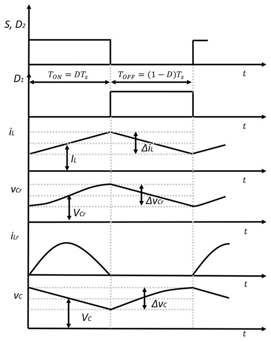
Figure 2.
Hybrid step−up converter main waveforms in CCM.
The three operation modes are presented in Figure 3. The operation mode is determined by the transistor on time with respect to the resonant period T0. In modes 1 and 2, the switching losses are low because the resonant current iLr naturally reaches zero, assuring zero current switching for diode D2. Mode 3 is to be avoided because the resonant current is nonzero at the time the transistor is switched off.
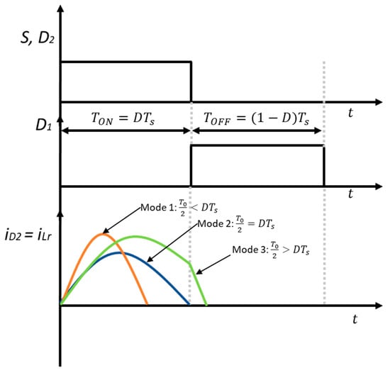
Figure 3.
Hybrid step−up converter. The three modes of operation.
The static conversion ratio of the hybrid switching step−up converter is [8]
Examining Equation (1), it is clear that the static conversion ratio cannot be smaller than 2. Furthermore, for the same duty cycle value, a larger output voltage can be obtained compared to the classical Boost converter. Additionally, the hybrid switching step-up converter also offers lower semiconductor voltage stresses and a lower dc current through the main inductor.
The converter modeling and the closed loop design is the main concern of this paper. The design example is for the hybrid switching step-up converter with the parameters given in Table 1.

Table 1.
Hybrid switching step−up converter parameters.
In order to design the controller for the hybrid step−up converter, first the control-to−output small-signal transfer function, Gc(s), needs to be determined.
For this purpose, two approaches are used. The practical approach uses impulse response analysis in the PLECS simulation program [20], whereas the analytical approach uses the time-varying transfer function proposed in [23,24]. The simulation schematic used for the impulse response analysis is depicted in Figure 4. As can be seen, a small-signal perturbation is added to the duty cycle d and the small-signal response of the converter is measured with the Vm1 voltage sensor.
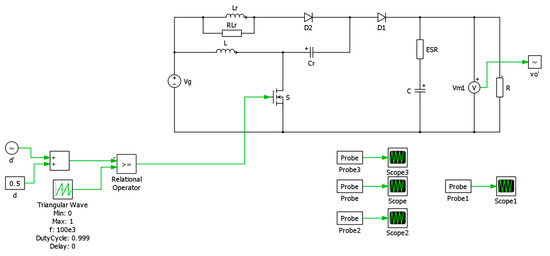
Figure 4.
Hybrid step−up converter PLECS schematic used for impulse response analysis.
The frequency vector used for the impulse response analysis consists of 400 logarithmically spaced frequency points ranging from 1 Hz to 50 kHz. For each frequency point, the magnitude and phase of the control-to-output transfer function are measured. The resulting two Bode plots are depicted in Figure 5.

Figure 5.
Hybrid step−up converter amplitude and phase characteristics obtained in PLECS.
In order to obtain an analytical transfer function as a ratio of two polynomials, the Bode data are imported to MATLAB. The frequency response complex vector is determined, denoting the magnitude vector and the phase vector as magnitude_PLECS [dB] and phase_PLECS [°], respectively.
Using the frequency response vector, the control-to-output transfer function is estimated using the tfest function available in MATLAB. In order to use this command, the number of poles needs to be provided as an input parameter. The hybrid-switching step-up converter is a fourth order system because it contains four reactive elements. Since the poles and zeros given by the resonant elements are much higher compared to the switching frequency, a second-order estimation of the control-to-output transfer function is considered sufficient, as it covers the frequency domain from dc up to half of the switching frequency. The resulting rational expression for the second order control-to-output transfer function is as follows:
It can be remarked that the transfer function contains a zero in the right half plane, similar to the classical boost topology. In Figure 6, both the PLECS data points and the estimated second-order transfer function are represented. It can be remarked that excellent overlapping is achieved.
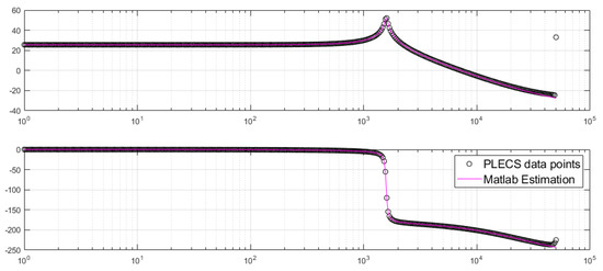
Figure 6.
Hybrid step−up converter PLECS data points versus MATLAB transfer function estimation.
An analytical approach for obtaining the control-to-output transfer function of the converter is given by the time varying transfer function [23,24]. This method leads to an exact small-signal model. Unfortunately, this approach does not provide a transfer function in a rational form. Moreover, an averaged model cannot be obtained from it using the Taylor expansion and retaining the first two terms because not all the state variables fulfill the small-ripple and slow-varying assumptions. However, this model is a valuable tool for validating the obtained control-to-output transfer function expression from (4).
In order to obtain the exact small-signal model, the state-space description of the hybrid step-up converter is required. The notations for the system variables and converter parameters are described in the nomenclature table found in the back part. The input vector u, the output vector y and the state vector x are defined below:
The state-space matrices of the hybrid step-up converter for the first topological state (resonant state), denoted with index 1, are
The state-space matrices for the second topological state (linear discharge) are denoted with indices 2. In order to avoid matrix singularity for A2, a large resistor RLr was added in parallel to the resonant inductor.
The algorithm in [23,24] for deriving the exact control-to-output transfer function is implemented in MATLAB. Similar to (3), the algorithm provides a complex number for each frequency value in the frequency vector. Figure 7 compares the Bode data obtained from PLECS (blue dots) to the exact transfer function values (magenta line). A good agreement can be remarked except for the zone around the resonant frequency where PLECS is predicting a higher quality factor. Anyway, the cutoff frequency will be chosen much higher than the resonant frequency, and therefore, this mismatch is not affecting the design.
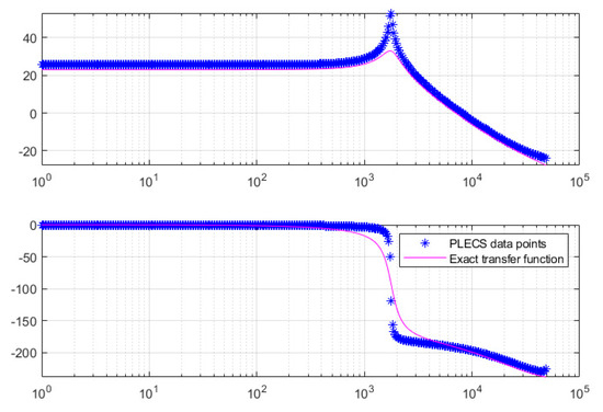
Figure 7.
Hybrid step−up converter PLECS data points versus time varying exact transfer function.
As the rational control-to-output transfer function previously determined is of second order, a type 3 amplifier is a suitable choice. The closed-loop small-signal model of the hybrid step-up converter is given in Figure 8 in its classical format. It consists of the control-to-output transfer function of the converter Gc(s) and the type 3 controller GAE3(s).
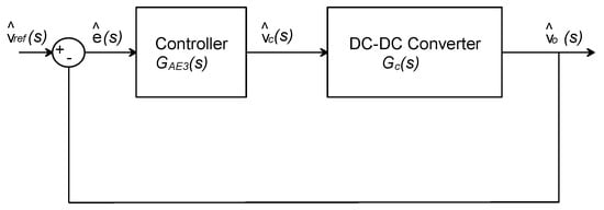
Figure 8.
Closed−loop small−signal model of the hybrid step−up converter.
The controller is designed using the pole-zero placement method presented in [25,26]. Examining Equation (4), it is clear that the control-to-output transfer function written in canonical form is
On the other side, the type 3 amplifier has the following expression:
The control-to-output and type 3 transfer function parameters are described in Table 2.
Table 2.
Control−to−output transfer function parameters.
The poles and zeros of the type 3 amplifier are chosen according to [25,26]:
where represents the angular switching frequency. The angular cutoff frequency is chosen such that the following condition is fulfilled:
The open-loop transfer function is depicted in Figure 9. It can be seen that a cutoff frequency, fC, of 3.7 kHz and a phase margin φm of 28° are achieved.
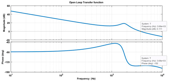
Figure 9.
Hybrid step−up converter open loop transfer function.
The next step is to discretize the controller transfer function GAE3(s). It is known that the discretization process of an analog controller needs to account for the loop delay caused by the sampling processes of the analog to digital converter and the pulse width modulator [27].
The loop delay does not impact the magnitude, but it considerably impacts the overall phase of the system. For this reason, it needs to be taken into account in the discretization process of the controller. In [27], it is shown that the loop delay is given by:
For the discretization of the designed type 3 controller, the Tustin transform (bilinear transform) is used as follows:
The sampling period, , of the digital filter is chosen to be equal to the switching period, . The sampling period chosen for discretization is much smaller than the cutoff frequency of the analog filter, and hence, prewarping is not necessary. Discretization is easily performed in MATLAB using the c2d command. The discretized controller GAE3d(z) transfer function is given in (14), and the coefficients are provided in Table 3.
Table 3.
Digital controller coefficients.
3. Results
In order to validate the digital controller, the converter was simulated in a closed loop. The simulation program used for this purpose is CASPOC [28]. The simulation schematic is presented in Figure 10.
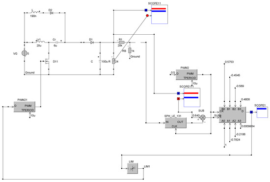
Figure 10.
Hybrid step−up converter closed loop simulation schematic.
The output voltage is first scaled by a voltage divider and then passed to a sample and hold block that performs sampling on the leading edge of the clock signal. This block emulates the analog to digital converter input that will be used in practice for monitoring the output voltage by the digital signal processor. The output of the sample and hold block is subtracted from the reference voltage and the error signal is passed through the digital controller. The direct form II [27] is used to implement the digital controller using minimum number of shift registers, as can be seen in Figure 11.
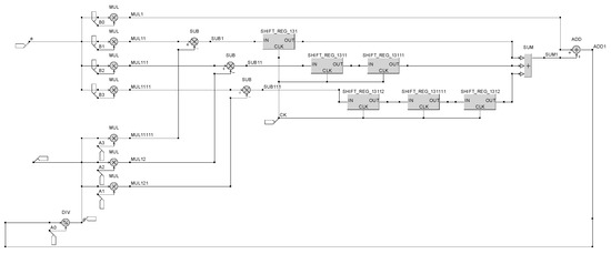
Figure 11.
Digital controller implementation in CASPOC using shift registers.
Figure 12 depicts the closed-loop response of the converter to a load step from 24 Ω to 15 Ω (Figure 12a) and from 15 Ω to 24 Ω (Figure 12b). This implies load current steps from 626 mA (corresponding to 24 Ω) to 751 mA (corresponding to 15 Ω). The output voltage is represented on the left Y-axis in [V], whereas the load current is represented on the right Y-axis in [mA]. In both plots, the output voltage is regulated to 15 V after the transient, as desired. Figure 13 shows the closed-loop response of the converter to a step change in the reference voltage. The output voltage is represented on the left Y-axis in [V], and the reference voltage is represented on the right Y-axis in [mV]. Figure 13a depicts the output voltage before and after a step change in the reference voltage from 0.643 V to 0.714 V, whereas Figure 13b presents the output voltage change to a step in the reference voltage from 0.714 V to 0.643 V. In both cases, the output voltage changes to the desired setpoint from 13.5 V to 15 V (Figure 13a) and then back from 15 V to 13.5 V (Figure 13b).
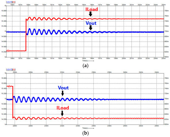
Figure 12.
(a) Closed−loop response of the converter to a load step from 24 Ω to 15 Ω. (b) Closed−loop response of the converter to a load step from 15 Ω to 24 Ω. The load current is marked with red, and the output voltage is marked with blue.
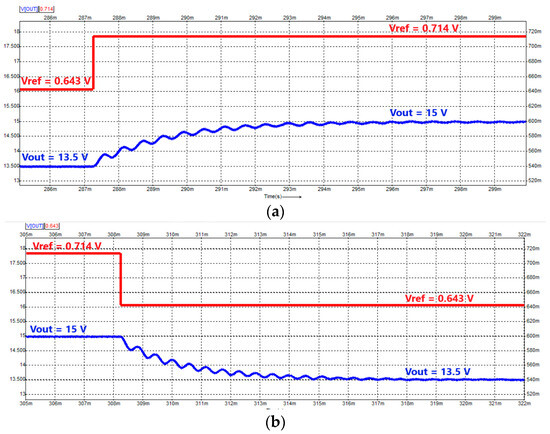
Figure 13.
(a) Closed−loop response of the converter to a step in the reference voltage from 0.643 V to 0.714 V. (b) Closed−loop response of the converter to a step in the reference voltage from 0.714 V to 0.643 V. The reference voltage is marked with red, and the output voltage is marked with blue.
In order to practically confirm the controller design, a converter prototype board was built. The digital controller was implemented using a Launchpad containing a TMS320F28379D DSP [22]. In order to design the closed-loop controller, the output voltage is needed. Therefore, a voltage divider and a 12-bit resolution ADC channel are used. Furthermore, Controller Area Network (CAN) Communication is implemented to facilitate real-time parameter control of the converter via a graphical user interface. The hardware setup is presented in Figure 14.
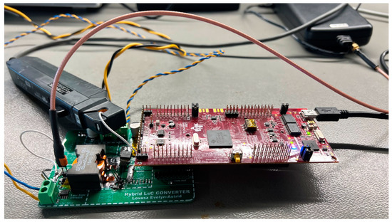
Figure 14.
The hybrid switching step−up converter prototype employing TMS320F28379D DSP for the digital controller.
For rapid prototyping, the code was implemented using Simulink Support Packages for C2000 Devices [29]. Figure 15a depicts the Simulink blocks used to generate the code. Four main software modules are addressed: the ADC module, the PWM module, the digital controller module and the controller area network (CAN) communication module. Figure 15b enfaces the graphical user interface (GUI). The CAN messages are sent between the GUI and the DSP such that the user can easily visualize and modify converter parameters. A switch is used to change between open- and closed-loop modes of operation.
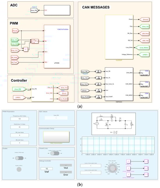
Figure 15.
(a) Simulink blocks used to generate the code for the 320F28379D DSP. (b) The GUI developed to easily modify the control parameters of the hybrid switching step−up converter.
Using this setup, the closed-loop converter response was analyzed. Figure 16a,b presents the way the converter output voltage responds to a load step. It can be remarked that in both cases in steady state the output voltage is not influenced by the load step, which proves good regulation, stability of the closed-loop system and the robustness of the controller. This behavior validates the design considerations for the digital controller. Compared to the ideal load step from simulation, the load current changes in 1.1 ms due to the time it takes the electronic dc load to change between the load resistance values 15 Ω and 24 Ω.
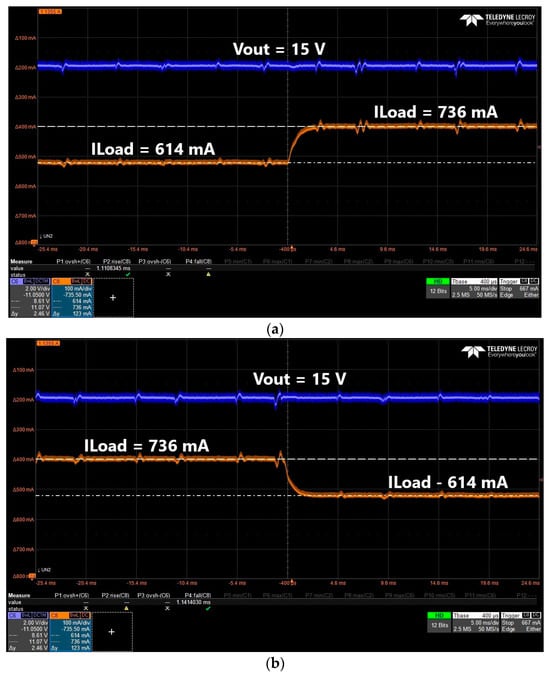
Figure 16.
(a) Converter output voltage (blue) before and after a step in the load (orange) from 614 mA to 736 mA. (b) Converter output voltage (blue) before and after a step in the load (orange) from 736 mA to 614 mA.
Figure 17 shows the converter response to a step change in the reference voltage.
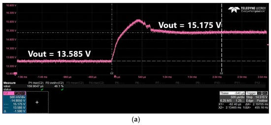
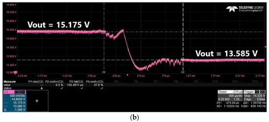
Figure 17.
(a) Closed−loop response of the converter to a step in the reference voltage from 0.643 V to 0.714 V. (b) Closed−loop response of the converter to a step in the reference voltage from 0.714 V to 0.643 V.
For the case in Figure 17a, the output voltage of the converter changes from 13.585 V to 15.175 V for a step in the reference voltage from 0.643 V to 0.714 V. An overshoot of 46.1% and a rise time of 159.9 µs are measured. For the case presented in Figure 17b, the output voltage changes from 13.585 V to 15.175 V for a step in the reference voltage from 0.714 V to 0.643 V. The overshoot is 9.3%, the undershoot is 37.6%, and the fall time is 135.4 µs. It can be concluded that the closed-loop system has a robust response which confirms the controller design.
4. Discussion
This paper presents a closed-loop application for a hybrid switching step-up converter, and several contributions are brought. Firstly, the state-space model of the hybrid switching converter is derived. Secondly, the small-signal transfer function of the converter is obtained both theoretically using the time varying transfer function and in simulation by using impulse response analysis in PLECS. For the best accuracy, the small-signal transfer function of the converter is theoretically obtained using the time-varying transfer function. As opposed to averaging techniques, the time-varying transfer function approach provides a control-to-output transfer function without frequency limitations. Both methods provide data point sets which are used for transfer function estimation in MATLAB. Thirdly, since the hybrid-switching step-up converter is of fourth order, the authors show that it can be approximated by a second-order transfer function for which well-established controller design methods can be employed. Consequently, a type 3 controller is designed and discretized for digital control of the hybrid-switching step-up converter. A first validation of the closed-loop behavior has been performed through simulation using the CASPOC program. Fourthly, the final validation of the digital controller and the closed-loop behavior of the hybrid-switching step-up converter on a practical prototype is presented. The digital controller is implemented on a development board using the TMS320F28379D DSP.
5. Conclusions
The paper adapts a well-known and straightforward method of designing a closed-loop application with a digital controller for higher-order dc-dc converters. A simple procedure for deriving the control-to-output transfer function is proposed. The digital controller can be rapidly and easily implemented using Simulink blocks from the C2000 Embedded Coder Support Package. The code is generated and deployed automatically on the DSP, and the digital controller can be easily tested for the high step-up converter with hybrid switching. The procedure was applied to a 5 V to 15 V/15 W/100 kHz hybrid fourth-order step-up converter, and the theoretical considerations were confirmed by the experimental results. This method can be easily extended to other higher-order converters.
Author Contributions
Conceptualization, E.-A.L.; Methodology, D.L. and S.L.; Software, E.-A.L.; Validation, E.-A.L.; Formal analysis, E.-A.L.; Resources, D.L.; Data curation, S.L.; Writing—original draft, S.L.; Writing—review & editing, S.L.; Supervision, D.L. All authors have read and agreed to the published version of the manuscript.
Funding
This work was supported by a grant of the Romanian Ministry of Research, Innovation and Digitalization, project number PFE 26/30.12.2021, PERFORM-CDI@UPT100—The increasing of the performance of the Polytechnic University of Timișoara by strengthening the research, development and technological transfer capacity in the field of “Energy, Environment and Climate Change” at the beginning of the second century of its existence, within Program 1—Development of the national system of Research and Development, Subprogram 1.2—Institutional Performance—Institutional Development Projects—Excellence Funding Projects in RDI, PNCDI III.
Data Availability Statement
Data are contained within the article.
Conflicts of Interest
The authors declare no conflict of interest.
Nomenclature
| T0 | resonant period |
| D | steady state duty cycle |
| perturbation in the continuous duty cycle | |
| Ton | transistor on time in steady state |
| Toff | transistor off time in steady state |
| Ts | switching period |
| fs | switching frequency |
| IL | filter inductor dc current |
| ΔiL | peak-to-peak filter inductor current ripple |
| iLr | instantaneous resonant inductor current |
| iD2 | instantaneous current through diode D2 |
| VC | filter capacitor dc voltage |
| ΔvC | peak-to-peak filter capacitor voltage ripple |
| vC | instantaneous filter capacitor voltage |
| VCr | resonant capacitor dc voltage |
| ΔvCr | resonant capacitor peak-to-peak voltage ripple |
| vCr | instantaneous resonant capacitor voltage |
| M | static conversion ratio |
| Vg | input dc voltage |
| vg | instantaneous input voltage |
| small signal perturbation in the variable z(t) | |
| Vo | output dc voltage |
| vo | instantaneous output voltage |
| R | load resistance |
| L | filter inductor |
| Lr | resonant inductor |
| C | filter capacitor |
| Cr | resonant capacitor |
| Gc(s) | continuous control-to-output transfer function |
| GAE3(s) | continuous type 3 controller transfer function |
| A1, B1, E1, F1 | state-space matrices for the first topological state |
| A2, B2, E2, F2 | state-space matrices for the second topological state |
| Gdelay(s) | continuous transfer function of the digital loop delay |
| tdelay | digital loop delay |
| Tsampling | sampling period |
| GAE3d(z) | discrete transfer function of the digital controller |
| a0, a1, a2, a3 | denominator coefficients of digital controller transfer function |
| b0, b1, b2, b3 | numerator coefficients of digital controller transfer function |
| ADC | analog to digital controller |
| CAN | controller area network |
| DSP | digital signal processor |
| PWM | pulse width modulation |
References
- Pop-Calimanu, I.-M.; Balint, M.; Lascu, D. A New Hybrid Ćuk DC-DC Converter with Coupled Inductors. Electronics 2020, 9, 2188. [Google Scholar] [CrossRef]
- Haider, Z.; Ulasyar, A.; Khattak, A.; Zad, H.S.; Mohammad, A.; Alahmadi, A.A.; Ullah, N. Development and Analysis of a Novel High-Gain CUK Converter Using Voltage-Multiplier Units. Electronics 2022, 11, 2766. [Google Scholar] [CrossRef]
- Hwu, K.-I.; Tseng, P.-C. High Step-Up Converter. Electronics 2023, 12, 4000. [Google Scholar] [CrossRef]
- Truong, V.-A.; Luong, X.-T.; Nguyen, P.-T.; Quach, T.-H. The Improvement Switching Technique for High Step-Up DC-DC Boost Converter. Electronics 2020, 9, 981. [Google Scholar] [CrossRef]
- Meshael, H.; Elkhateb, A.; Best, R. Topologies and Design Characteristics of Isolated High Step-Up DC–DC Converters for Photovoltaic Systems. Electronics 2023, 12, 3913. [Google Scholar] [CrossRef]
- Cuk, S. Hybrid Switching Step-Down Converter with a Hybrid Transformer. U.S. Patent 9,231,471 B2, 5 January 2016. [Google Scholar]
- Lovasz, E.-A.; Lascu, D. A New Buck Converter with Hybrid Switching. In Proceedings of the 2020 International Symposium on Electronics and Telecommunications (ISETC), Timisoara, Romania, 5–6 November 2020; IEEE: Piscataway, NJ, USA, 2020; pp. 1–4. [Google Scholar] [CrossRef]
- Ciresan, A.; Lica, S.; Lascu, D.; Tomoroga, M. A novel low-stress high-efficiency step-up DC-DC converter. In Proceedings of the 2015 19th International Conference on System Theory, Control and Computing (ICSTCC), Cheile Gradistei, Romania, 14–16 October 2015; IEEE: Piscataway, NJ, USA, 2015; pp. 830–835. [Google Scholar] [CrossRef]
- Zhou, D. Synthesis of PWM Dc-to-Dc Power Converters; California Institute of Technology: Pasadena, CA, USA, 1995. [Google Scholar]
- Jiang, W.; Sun, L.; Chen, Y.; Ma, H.; Hashimoto, S. A Hardware-in-the-Loop-on-Chip Development System for Teaching and Development of Dynamic Systems. Electronics 2021, 10, 801. [Google Scholar] [CrossRef]
- Salimi, M. A Novel Approach for Adaptive Partial Sliding Mode Controller Design and Tuning in Non-Minimum Phase Switch-Mode Power Supplies. Electronics 2023, 12, 1438. [Google Scholar] [CrossRef]
- Rwamurangwa, E.; González, J.D.; Saiz, P.J.V.; Martín-Ramos, J.A.; Pernía, A.M. A Parallel Resonant Converter Polynomial Model Implemented in a Digital Signal Controller. Electronics 2022, 11, 1085. [Google Scholar] [CrossRef]
- Lamo, P.; Azcondo, F.J.; Pigazo, A. Academic Use of Rapid Prototyping in Digitally Controlled Power Factor Correctors. Electronics 2022, 11, 3600. [Google Scholar] [CrossRef]
- Kroičs, K.; Staņa, Ģ. Bidirectional Interleaved DC–DC Converter for Supercapacitor Energy Storage Integration with Reduced Capacitance. Electronics 2022, 12, 126. [Google Scholar] [CrossRef]
- Lee, G.-Y.; Park, H.-C.; Ji, M.-W.; Kim, R.-Y. Digitalized Control Algorithm of Bridgeless Totem-Pole PFC with a Simple Control Structure Based on the Phase Angle. Electronics 2023, 12, 4449. [Google Scholar] [CrossRef]
- Kirei, B.S.; Farcas, C.-A.; Chira, C.; Ilie, I.-A.; Neag, M. Hardware Emulation of Step-Down Converter Power Stages for Digital Control Design. Electronics 2023, 12, 1328. [Google Scholar] [CrossRef]
- Lamo, P.; De Castro, A.; Sanchez, A.; Ruiz, G.A.; Azcondo, F.J.; Pigazo, A. Hardware-in-the-Loop and Digital Control Techniques Applied to Single-Phase PFC Converters. Electronics 2021, 10, 1563. [Google Scholar] [CrossRef]
- Merchan-Villalba, L.R.; Lozano-Garcia, J.M.; Gonzalez-Longatt, F.; Ramirez-Arredondo, J.M.; Pizano-Martinez, A.; Avina-Cervantes, J.G. Low-Cost Real-Time Control Platform with Embedded Isolated Electrical Sensors for Power Electronics. Electronics 2023, 12, 3320. [Google Scholar] [CrossRef]
- MathWorks, Natick, Massachusetts, United States. MATLAB. MathWorks. Available online: https://www.mathworks.com/products/matlab.html (accessed on 25 April 2024).
- PLECS, Zurich, Switzerland. Available online: https://www.plexim.com/products/plecs (accessed on 25 April 2024).
- B-G474E-DPOW1. Available online: https://www.st.com/en/evaluation-tools/b-g474e-dpow1.html (accessed on 25 April 2024).
- Texas Instruments, Dallas, Texas, United States, LAUNCHXL F28379D. Available online: https://www.ti.com/tool/LAUNCHXL-F28379D (accessed on 25 April 2024).
- Tymerski, R. Frequency Analysis of Time-Interval-Modulated Switched Networks. IEEE Trans. Power Electron. 1991, 6, 287–295. [Google Scholar] [CrossRef]
- Tymerski, R. Application of the time-varying transfer function for exact small-signal analysis. IEEE Trans. Power Electron. 1994, 9, 196–205. [Google Scholar] [CrossRef]
- Ridley, R.B. Power Supply Design; Ridley Designs: Monpazier, France, 2012. [Google Scholar]
- Basso, C.P. Transfer Functions of Switching Converters: Fast Analytical Techniques at Work with Small-Signal Analysis; Faraday Press: Apache Junction, AZ, USA, 2021. [Google Scholar]
- Erickson, R.W.; Maksimović, D. Fundamentals of Power Electronics; Springer International Publishing: Cham, Switzerland, 2020. [Google Scholar] [CrossRef]
- Simulation Research. CASPOC, Alphen aan den Rijn, The Neatherlands. Available online: https://www.caspoc.com/ (accessed on 25 April 2024).
- Mathworks, Natick, Massachusetts, United States, Support Packages for Texas Instruments devices. Available online: https://www.mathworks.com/hardware-support/texas-instruments.html (accessed on 25 April 2024).
Disclaimer/Publisher’s Note: The statements, opinions and data contained in all publications are solely those of the individual author(s) and contributor(s) and not of MDPI and/or the editor(s). MDPI and/or the editor(s) disclaim responsibility for any injury to people or property resulting from any ideas, methods, instructions or products referred to in the content. |
© 2024 by the authors. Licensee MDPI, Basel, Switzerland. This article is an open access article distributed under the terms and conditions of the Creative Commons Attribution (CC BY) license (https://creativecommons.org/licenses/by/4.0/).