Abstract
New SPICE-compatible circuit models of a multiport are presented here that are suitable for the frequency-domain and time-domain analyses of hybrid systems containing linear distributed elements and possibly non-linear lumped elements. Distributed elements models are based on scattering parameters with potentially complex reference impedances, which are not necessarily equal for all ports. Both exact and approximated (lumped) models are proposed. The scattering parameters are directly taken as the model element values in the former case. In the latter case, the model element values are equal to the real and imaginary parts of the poles and residues of the rational approximation. The models comprise a multiport (with an admittance matrix numerically equal to the modeled scattering matrix or approximating it) equipped with a pair of coupled impedances at each port. A few examples validate the proposed approach and prove its efficiency in terms of matrix size and analysis time compared to some selected commercial counterparts.
1. Introduction
This introductory section is designed to provide the motivation and an overview of the present work. In microwave engineering, it is often necessary to simulate hybrid systems that combine lumped and distributed elements. In the case of an extensive lumped part, especially when it is non-linear, universal SPICE-like simulators appear to be the optimal tool. The distributed part of the system is usually described by its scattering parameters, which are defined in the frequency domain. The scattering parameters can be derived from measurements by a vector network analyzer or simulations of the electromagnetic field using such programs as Advanced Design System (ADS), CST Studio Suite, or QuickWave. Unfortunately, scattering parameters cannot be used in most SPICE-like circuit simulators. However, several solutions (mainly commercial) have been known for a long time to meet the need to simulate hybrid systems. These include the following:
- The HSPICE program [1] can import files in the Touchstone (SnP) format, which describes multiports in terms of their scattering parameters.
- The application note for the MicroSim program [2] describes a two-port model using behavioral sources (only available in some versions of SPICE) and contains the source code of the BASIC program, generating the appropriate input file for SPICE. This approach was generalized in [3] for multiports with different (but real) reference impedances of each port.
- The Ansys HFSS program [4] is capable of generating a circuit description compatible with the generic SPICE program, as it does not require behavioral sources. However, it is an approximate model. A finite partial fraction expansion is employed to approximate the frequency characteristics of the scattering parameters. Being rational functions, these approximations can be implemented as a lumped system composed of RC elements and controlled sources.
- The RF Toolbox for the MATLAB R2023b environment from Mathworks [5] can generate a similar approximation of the scattering parameters (loaded from a file in the Touchstone S2P format) and then create a description of the lumped circuit compatible with the generic SPICE program. However, in the current version of the package, this last step requires the renormalization of the scattering parameters to the identical reference impedances for all ports. The free scikit-rf package for Python (currently 3.7+) [6] has similar capabilities.
The aforementioned SPICE-compatible models of the multiports described by scattering parameters present a few areas for improvement. Many of these models are only suitable for reference impedances that are real or equal for all ports. Even if complex reference impedances are allowed, it is not always clear which definition of waves is being used, and the model is only compatible with one such definition. The models are typically constructed without sufficient attention being directed to the use of only those elements that are best suited to the modified nodal analysis paradigm, such as voltage-controlled current sources. Consequently, the obtained circuits are unnecessarily complex, leading to longer simulation times. Finally, the expressions for the model element values are often sophisticated and require significant effort to compute them. In the present paper, we aim to address some of these issues.
The objective of this work is to present a method for the analysis of hybrid lumped/distributed systems that makes use of freely available tools while taking into account the following requirements:
- The reference impedances for scattering parameters may be arbitrary, including being complex, frequency-dependent, and distinct for individual ports.
- It is possible to perform a frequency-domain analysis at multiple frequency points and a time-domain analyses, provided that the distributed part of the system is linear.
- High simulation efficiency is achieved through the model’s canonical number of internal nodes. The behavioral model proposed below introduces a single internal node for each port, and the number of additional internal nodes per port required by the approximate lumped model proposed below is equal to the number of poles. The small number of internal model nodes translates into small sizes of the matrices describing the circuit and, consequently, short analysis times. This is especially important when modeling interconnections that often have several dozen ports.
- Ease of use due to the direct utilization of available numerical data:
- (a)
- Regarding exact models using scattering parameters, the behavioral source parameters should be directly equal to the figures in SnP files without the necessity of renormalizing the scattering parameters or applying additional conversions. Although prior renormalization is sometimes recommended in the analysis of microwave networks [7], the renormalization formulas (see refs. [8,9,10]) are so complex that, in the author’s opinion, it is preferable to refrain from using them.
- (b)
- For lumped models based on rational approximations, the model elements’ values should be directly numerically equal to the poles or residues of the partial fraction expansion.
- The model is local in the sense that all model elements dependent on the reference impedance of a given port are as few as possible and appear only locally at this port. This feature will allow for the efficient simulation of systems where the reference impedances are different for each port and are complex and frequency-dependent.
The initial three requirements were already met by the model described in the author’s previous work [11]. Those models were based on a global description of the modeled multiport derived by appropriate manipulations of the matrix equations of the augmented and then restored network. However, the models introduced in [11] only had exact variants based on behavioral sources, so they were not suitable for a generic version of SPICE. The method of calculating the parameters of the models was complicated and required the use of appropriate software tools because the reference impedances of the ports influenced all values of the model elements. Moreover, although models were presented for both scattering parameters based on pseudo-waves and power waves, a definition of pseudo-waves adopted in [11] is rare in the literature. This problem is addressed in Section 2 and Section 3 below.
The fundamental concept underlying the multiport models proposed in [11] and in this study is the representation of incident and reflected waves as voltages and currents of a fictitious internal multiport. The admittance matrix of this internal multiport is closely related to the scattering parameters. Each port of the internal multiport is connected to a two-port, transforming its voltages and currents (proportional to the incident and reflected waves, respectively) into the voltages and currents of the modeled multiport.
In the present research, a family of behavioral models has been derived in a way completely different than previously (see Section 2). The direction of reasoning was reversed compared to [11]. Firstly, the straightforward global scaling of scattering parameters was assumed, and then the local equations of each transforming two-port were derived. Consequently, each scattering parameter has the same real and frequency-independent scaling coefficient. Although the models obtained in this way (presented in Section 5.1) have an identical (canonical) structure to some models proposed in [11], they feature completely different element values. The behavioral sources are described in tabular form, directly containing the numerical values of the scattering parameter taken from SnP files. The reference impedance of a port has only a local impact on the values of model elements, affecting only the single corresponding transforming two-port mentioned above and described in detail in Section 4. Consequently, all the stated requirements have been met.
During the tests of the currently proposed tabular behavioral models (see Section 7), it was discovered that although their frequency analysis yields perfectly accurate results, the accuracy holds only as long as the analysis is limited to the frequencies that are a subset (not necessarily proper) of the set of frequencies for which the scattering parameters were defined. Unfortunately, if one wants to reach beyond this set (and, for example, interpolate data for a finer frequency grid), problems arise. To prevent the interpolation process from generating erroneous results, it is necessary to unwrap the phase data of the scattering parameters. This necessitates the use of additional software tools, contravening requirement 4(a) (see page 2) of the direct use of the numerical values of scattering parameters contained in the SnP file. Upon examination of larger systems, another issue became evident. Even in the absence of interpolation, the tabular behavioral sources are implemented inefficiently, resulting in a considerable time of frequency-domain analysis.
Further complications arose in the time-domain analysis of a system described de facto by frequency parameters. Simulation programs (e.g., LTSPICE [12]) frequently employ the FFT algorithm in such a case. However, the heuristics for selecting the range of transformed frequencies and the frequency step do not always function as intended. Even the manual selection of these parameters may be inadequate because the method requires that the magnitude characteristic decrease to zero within the transformed frequency range. In the case of many low-loss systems, this condition is met only for unrealistically high frequencies. Consequently, the results of the time-domain analysis may differ significantly from reality, even if the system is excited with a signal with a well-defined and narrow frequency band (such as a Gaussian pulse).
Other issues may be caused by the non-causal nature of the available scattering parameters, resulting from the uncertainty of their measurements or the numerical errors of the electromagnetic field simulation. These problems can be avoided by using a rational approximation of the scattering parameters, which leads to approximate lumped models of distributed systems. Therefore, such approximate models are also derived and evaluated in Section 5.2. It is demonstrated that these models provide a shorter analysis time than the author’s exact (behavioral) models and other models known from the literature (with the same number of rational approximation poles) as concluded in Section 8.
To summarize the preceding remarks, the principal objective of this paper is to propose two kinds of circuit models, both exact and based on rational approximation, for the multiport described by arbitrarily defined scattering parameters with arbitrary reference impedances. The models employ only voltage-controlled current sources as active elements and thus are well suited for SPICE-like circuit simulators. The values of the elements are directly given by the scattering parameters or the poles and residues of their rational approximation. Moreover, the number of additional nodes introduced by the models is minimal, and the influence of reference impedances on element values is only local.
The following is an outline of the remaining portion of the paper. Section 2 contains the derivation of the proposed architecture of the multiport model, which comprises an inner multiport surrounded by so-called transforming two-ports at each port. Various definitions of scattering parameters encountered in the literature are presented and discussed in Section 3. These parameters influence the aforementioned transforming two-ports, so in Section 4, the models of such two-ports corresponding to the most prevalent definitions are derived. In Section 5, the structure of the inner multiport is derived and presented in two genres: the exact one, which requires behavioral sources, and the one based on the rational approximation of the scattering parameters, which uses only conventional voltage-controlled current sources. Section 6 contains a few examples. The first three are very simple and have a rather theoretical nature—they verify the correctness of the derived models analytically. The fourth example is a real-world one and is used in Section 7 to investigate the efficiency of the proposed model in terms of accuracy, analysis time, and memory requirements compared to some existing counterparts. The results of the current work are concluded in Section 8.
2. Derivation of the Model Structure
This section is dedicated to the presentation of the derivation of the proposed model structure. The fact that the exact models proposed below have the same structure as that of [11] (although with different element values) may erroneously suggest that the present work is merely a straightforward extension of [11]. Nevertheless, the novel derivation of the current model, which is not based on the augmented network concept, and the anticipated advantages over the previous one appear to justify its presentation to a broad audience of those interested in the simulation of mixed-type networks described by both scattering and circuit variables.
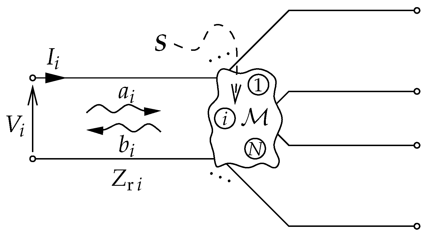
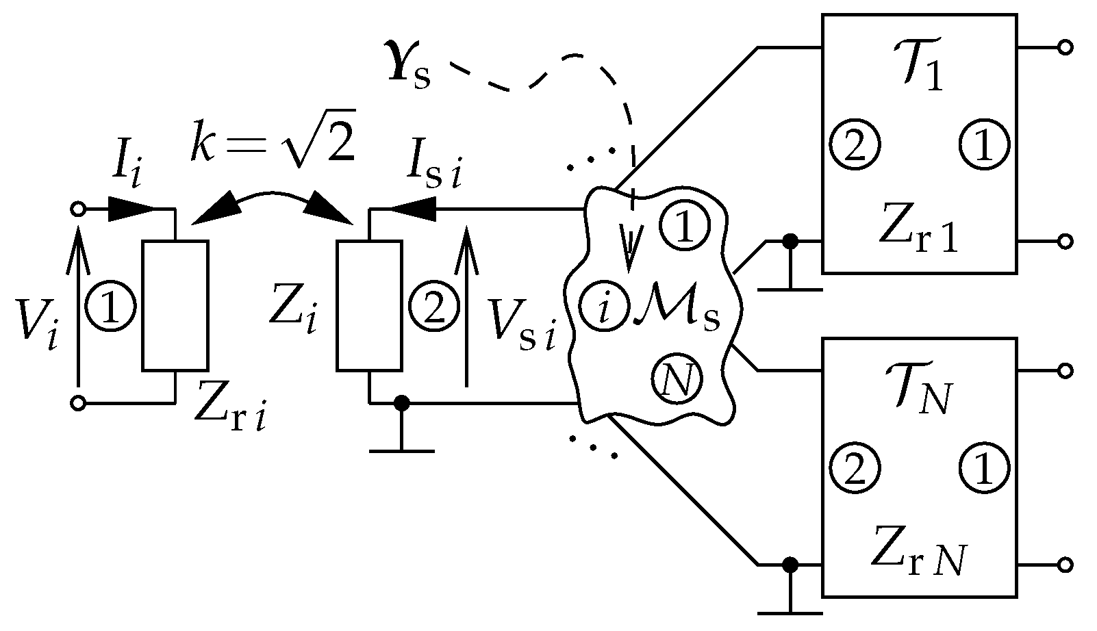
The scattering matrix of the modeled multiport containing N ports (see Figure 1) will be realized (up to the sign and the physical dimensions) as the admittance matrix of an internal multiport presented in Figure 2. It is intuitive that the incident waves and reflected waves should be numerically equal to the voltages and currents of this internal multiport. The only reference known to the author that represents both incident and reflected waves as voltages is [13]. It should be noted, however, that it is rarely necessary to calculate the incident and reflected waves. The simulation typically determines just the voltages and currents of a hybrid system comprising both lumped and distributed elements. Therefore, we will further assume that the incident and reflected waves will not be identical to but proportional to the internal multiport voltages and currents, respectively. To this end, we will assume (as an additional degree of freedom) a dimensionless proportionality factor common to the entire multiport , which can take real or complex values. This additional degree of freedom will simplify the model. The proportionality factor will be chosen to make the two-ports transforming circuit quantities ( and ) into wave quantities ( and , respectively) reciprocal. Additionally, to obtain appropriate physical dimensions of the considered quantities, an arbitrary positive scaling resistance common to all ports, will be introduced. For example, this could be equal to :
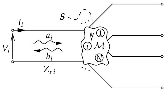
Figure 1.
N-port described by the scattering matrix . Port numbers are given inside circles. Circuit variables and wave variables based on the reference impedance , possibly complex, are presented for the i-th port.
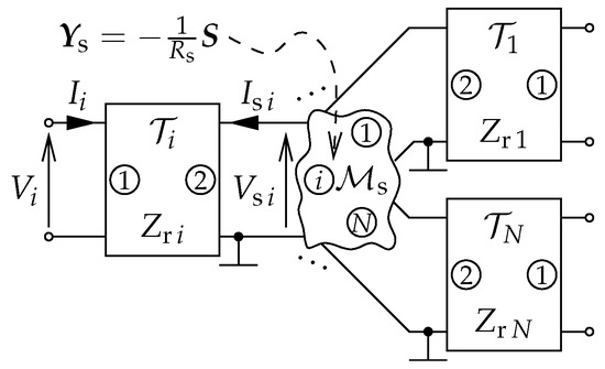
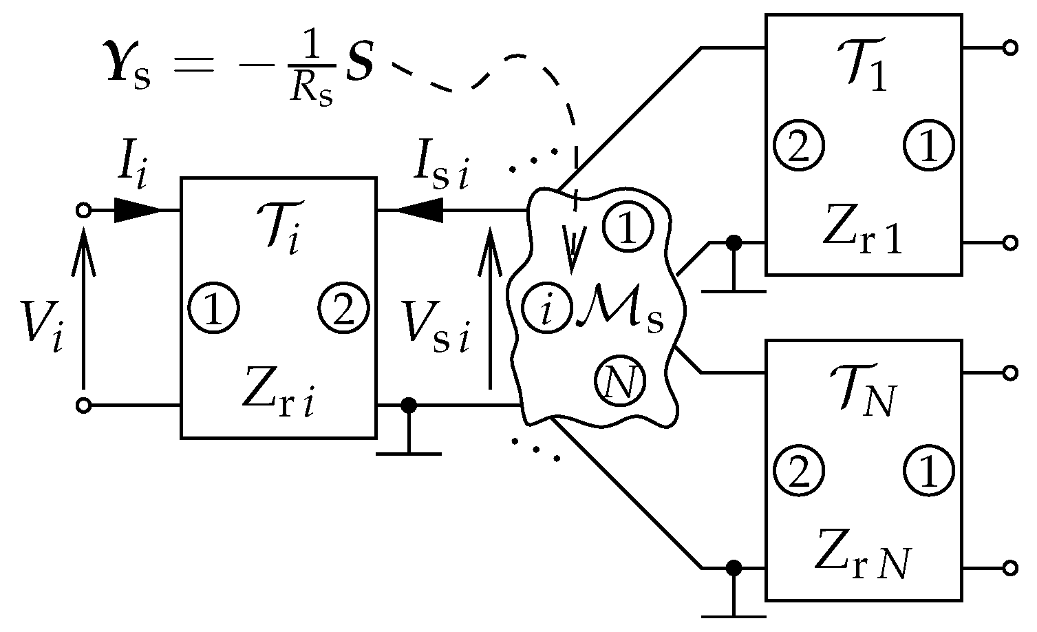
Figure 2.
Model of the N-port , which consists of a grounded inner N-port (described by the admittance matrix ) and transforming two-ports at each port. Port numbers are given inside circles. Variables and , proportional to the wave variables and , respectively, according to (1), are presented for the i-th port.
Given that the equations relating the circuit quantities (voltages and currents of the ports of the modeled multiport ) to the wave quantities (incident waves and reflected waves , and the voltages and currents of the ports of the internal multiport , which are proportional to the waves) are linear and homogeneous, it is possible to define a linear two-port for each port i as illustrated in Figure 2. A similar structure (but with different two-ports ) was developed in [14]. The two-port transforms the circuit quantities and at its primary (outer) port into the wave-related quantities and at its secondary (inner) port, which is connected to the internal multiport . Transforming two-ports will be further described in terms of their chain, impedance, or admittance matrices. All these matrices for the transforming two-port depend on the reference impedance and on the proportionality factor . The reference impedances can differ for each port and can be complex and frequency-dependent. We will only assume that they are non-zero and have non-negative real parts: .
Let us invert Equation (1) to the form
By taking the wave formula into the second equation of (1) and inserting the vector as in the first equation of (2), one obtains the admittance equations of the inner multiport :
It should be noted that the directions of the currents in Figure 2 cause the minus sign in (3). Thus, the admittance matrix of is directly related to the scattering matrix . For the obvious choice , both matrices are numerically equal, i.e., .
Figure 2 illustrates the most significant advantage of the approach presented here over the author’s previous proposal [11]: only one transforming two-port connected to the corresponding port depends on a given reference impedance. Consequently, the influence of the reference impedance is local. The admittance parameters of the internal multiport are solely dependent on the scattering parameters of the modeled multiport. Therefore, the scattering parameters (either measured or modeled and saved, e.g., in SnP files) can be utilized directly in the model proposed here. In contrast, the previous approach (cf. [11]) involved laborious calculation of the admittance parameters of the internal multiport, which depended on the reference impedances of all ports. It should be noted, however, that the current and prior models would become identical if all reference impedances were positive real and all equal to the scaling resistance: .
3. Definitions of Scattering Parameters
The literature contains various definitions of wave quantities and the corresponding scattering parameters. The first definition, historically, refers to the power waves [8,15,16,17], which are convenient for maximizing the power transfer. Regarding computer programs for electromagnetic field simulation, it is more natural to consider traveling waves [18]. Finally, using so-called pseudo-waves is more convenient when referring to microwave measurements [18]. Numerous review papers attempt to explain these differences [7,19,20,21,22]. All incident and reflected wave definitions can be written as a unified formula:
The factor in the denominators results from defining circuit quantities in this work as complex amplitudes rather than RMS values. Various definitions of the function of the reference impedance appearing in Formula (4) can be found in the literature as summarized in Table 1. The definition of the function referring to voltage waves given in [23] (4.58), which is a constant independent of , is intentionally omitted in the present paper. The square root in Table 1 is always defined as positive or with a positive real part. The diamond symbol ⋄ in (4) represents either the complex conjugate * (for power waves) or the identity (otherwise).

Table 1.
Various definitions of function encountered in the literature.
To facilitate the discussion, we will further denote the various definitions of wave quantities with the number from the first column of Table 1, with possibly an asterisk in the upper index if we choose the power wave variant. However, for this work, we will limit ourselves to only the three most essential definitions out of eight: classical power waves (denoted as definition ), classical pseudo-waves (denoted as definition 2), and the variant of pseudo-waves considered in the author’s previous work [11] (denoted as definition 4). The latter case is referred to in [22] as traveling waves. However, this does not agree with the definition of traveling waves presented in the seminal work [18], even if the reference impedances were to be equal to the corresponding characteristic impedances.
4. Models of the Transforming Two-Ports
4.1. Models for the Pseudo-Waves
In the case of pseudo-waves, the diamond symbol represents the identity and can be omitted. By adding and subtracting both sides of the formulas in (4), we obtain:
Then, by inverting these relationships, we obtain:
Considering Equation (2), we finally obtain:
These are the chain equations of the transforming two-port . Therefore, its chain matrix equals:
and its determinant is given by:
The determinant is independent of the choice of the scaling resistance .
In the case of the modified definition of pseudo-waves (definition 4), the determinant will simplify to the form:
For a proportionality factor , it will be equal to unity. The unitary determinant of the chain matrix indicates that the transforming two-port will be reciprocal.
In turn, for the classical pseudo-waves definition (definition 2), the determinant is given by:
and becomes equal to unity for the complex proportionality factor . Adopting such a value of the proportionality factor necessitates the additional assumption that the real part of the reference impedance is positive: (which is not the case, for example, for a purely imaginary reference impedance characteristic of evanescent propagation modes [25] (p. 1921) or in the case of inductively loaded waveguides [26]). Nevertheless, the same assumption was already necessary for the classical pseudo-waves definition (see [18] ((55)–(56))).
It is essential to recognize that the selection of the proportionality factor ensures that the chain matrix will be identical in both scenarios (for pseudo-waves definitions 2 and 4):
Consequently, an identical reciprocal two-port will transform circuit quantities into the quantities proportional to pseudo-waves, regardless of whether the waves are defined in a classical or modified manner. The only differences will manifest in the formulas for the possible reconstruction of the incident and reflected waves based on the port voltages and currents of the internal multiport (if there is a need to calculate these waves). The impedance and admittance matrices of the transforming two-port can also be determined based on the chain matrix:
and
Due to the reciprocity of the transforming two-port, these matrices have a simple structure that facilitates their circuit implementations.
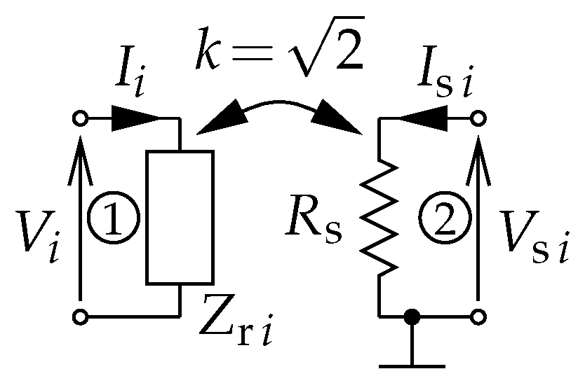
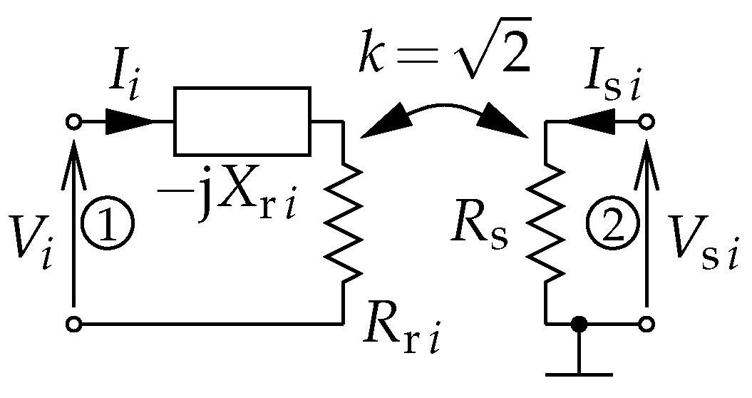
The form of the impedance matrix (13) is essential in this context because it closely resembles the impedance matrix of a pair of coupled inductances. The circuit implementation is, therefore, in the form of a reference impedance coupled to a scaling resistance with a coupling coefficient equal to the square root of two as shown in Figure 3. The non-physical value of the coupling coefficient (larger than unity) is not a problem here, as it only applies to the model of the system and is fully justified in simulations. Coupled impedances are a real-world concept [27] (Section II.B). They are a primary element in some computer analysis programs for electronic circuits, e.g., NAP2 [28]. In other programs (e.g., those from the SPICE family), they can be implemented as follows.

Figure 3.
A model of the transforming two-port for pseudo-waves, corresponding to the i-th port with the reference impedance , consisting of two coupled impedances with the coupling coefficient k. Primary and secondary port numbers are given inside circles.
- Two impedances connected by a negative impedance inverter implemented in the form of two current-controlled voltage sources with complex trans-admittances (Figure 4);
- The Norton equivalent of the above model (Figure 5);
- The T-type two-port, if necessary, supplemented with an ideal transformer with a 1:1 winding ratio connected to the primary port, which will ensure regularity conditions of the connection (Figure 6);
The ideal transformers depicted in Figure 6 and Figure 7 are superfluous if the i-th port of the modeled multiport is grounded.

Figure 4.
A Thévenin form of the model of the transforming two-port for pseudo-waves, corresponding to the i-th port with the reference impedance , containing a symmetric negative impedance inverter (NIV) realized using current-controlled voltage sources. The mutual impedance .
Figure 4.
A Thévenin form of the model of the transforming two-port for pseudo-waves, corresponding to the i-th port with the reference impedance , containing a symmetric negative impedance inverter (NIV) realized using current-controlled voltage sources. The mutual impedance .
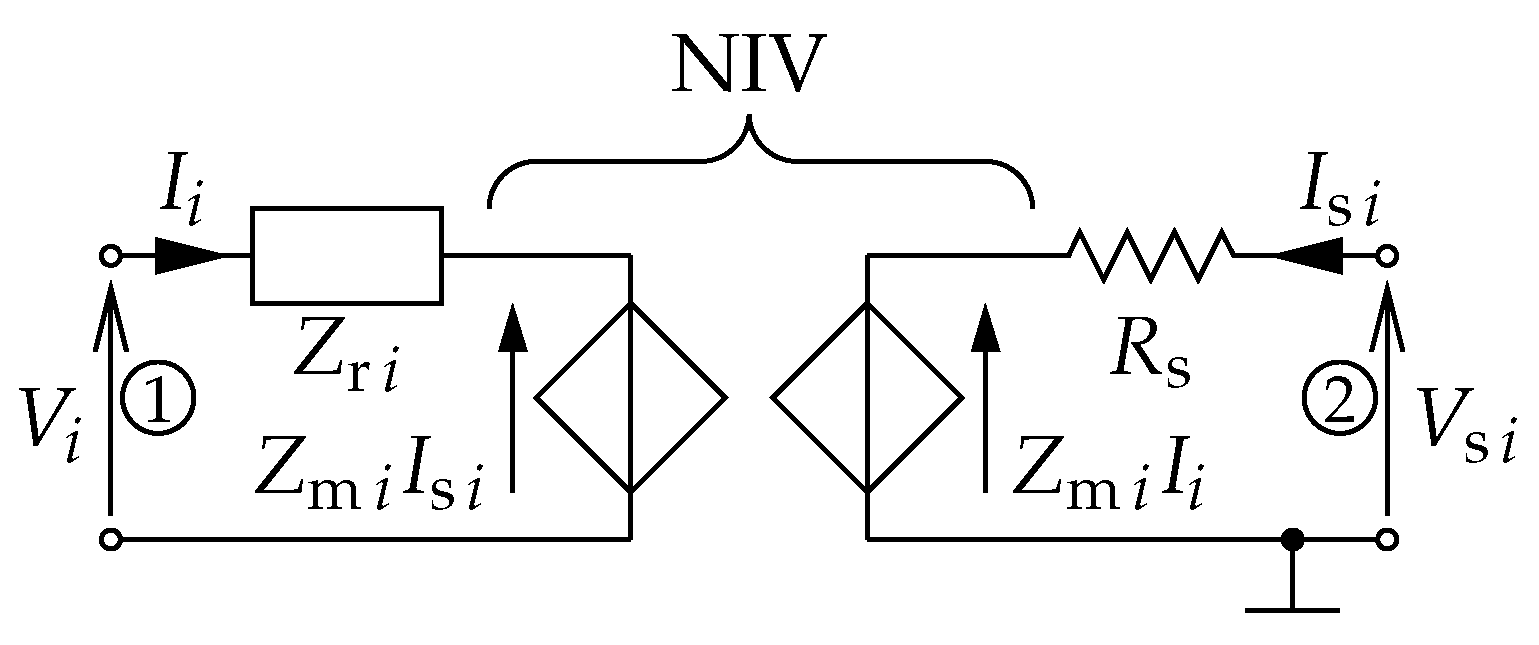
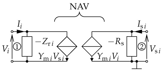
Figure 5.
A Norton form of the model of the transforming two-port for pseudo-waves, corresponding to the i-th port with the reference impedance , containing a symmetric negative admittance inverter (NAV) realized using voltage-controlled current sources. The trans-admittance .
Figure 5.
A Norton form of the model of the transforming two-port for pseudo-waves, corresponding to the i-th port with the reference impedance , containing a symmetric negative admittance inverter (NAV) realized using voltage-controlled current sources. The trans-admittance .
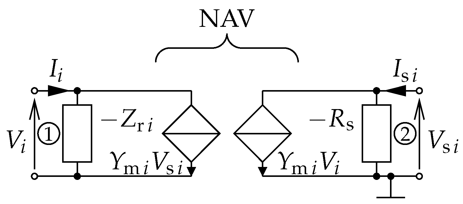
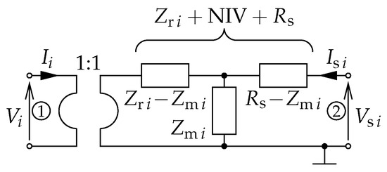
Figure 6.
A model of the transforming two-port for pseudo-waves, corresponding to the i-th port with the reference impedance , containing a symmetric negative impedance inverter (NIV) realized using a T-type two-port and an ideal transformer. The mutual impedance .
Figure 6.
A model of the transforming two-port for pseudo-waves, corresponding to the i-th port with the reference impedance , containing a symmetric negative impedance inverter (NIV) realized using a T-type two-port and an ideal transformer. The mutual impedance .
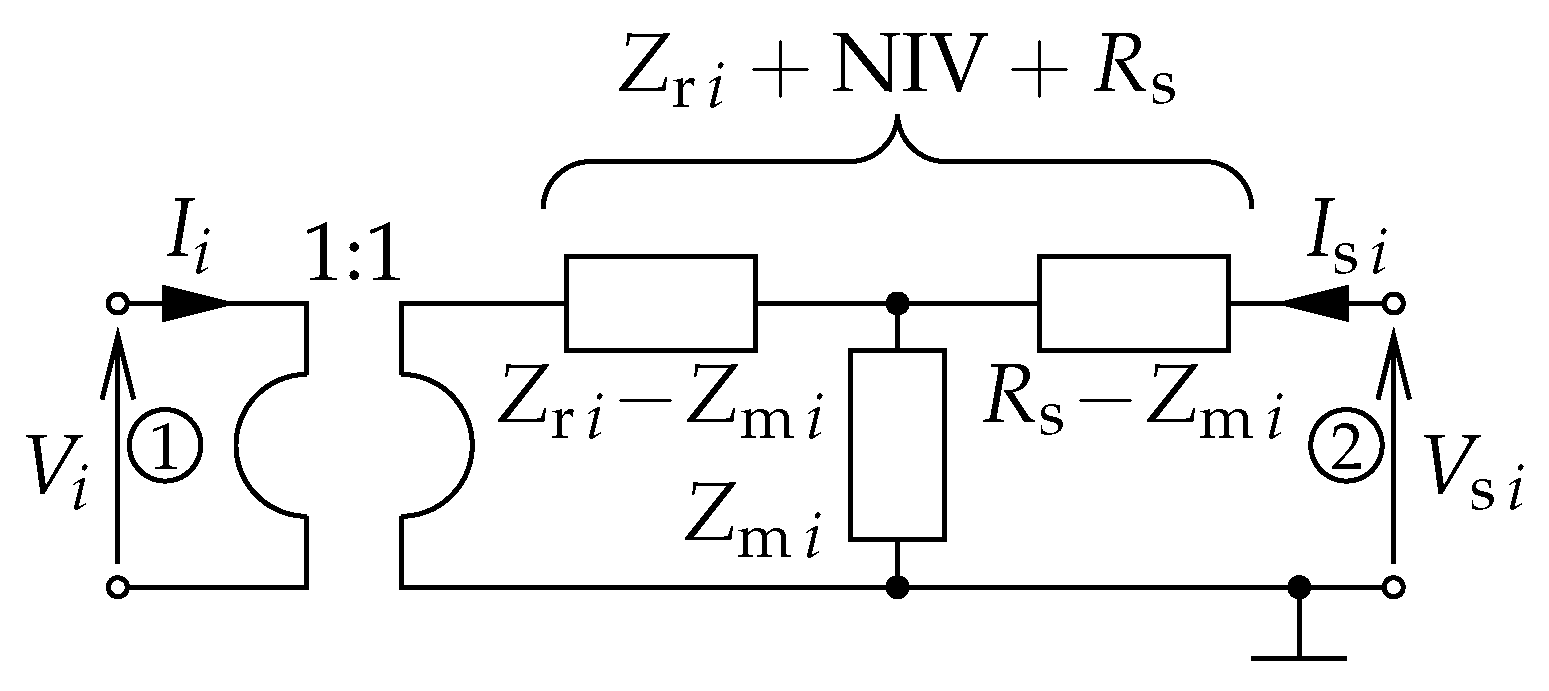
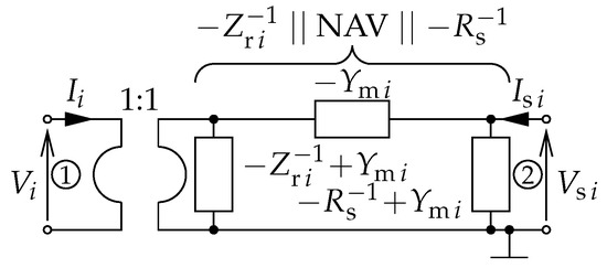
Figure 7.
A model of the transforming two-port for pseudo-waves, corresponding to the i-th port with the reference impedance , containing a symmetric negative admittance inverter (NAV) realized using a -type two-port and an ideal transformer. The trans-admittance . Element admittances are given.
Figure 7.
A model of the transforming two-port for pseudo-waves, corresponding to the i-th port with the reference impedance , containing a symmetric negative admittance inverter (NAV) realized using a -type two-port and an ideal transformer. The trans-admittance . Element admittances are given.

The models shown in Figure 4, Figure 5, Figure 6 and Figure 7 are relatively simple. However, they have practical significance mainly in the case of a real reference impedance. A different approach can be used when the reference impedance is complex and frequency-dependent. This is based on the results presented in Section 5 below, which deals with the exact (Section 5.1) or approximate (Section 5.2) implementation of the arbitrary inner multiport described by its admittance matrix . Tailoring these results to the case where the inner multiport is the transforming two-port described by the admittance matrix defined by (14) gives the desired model.
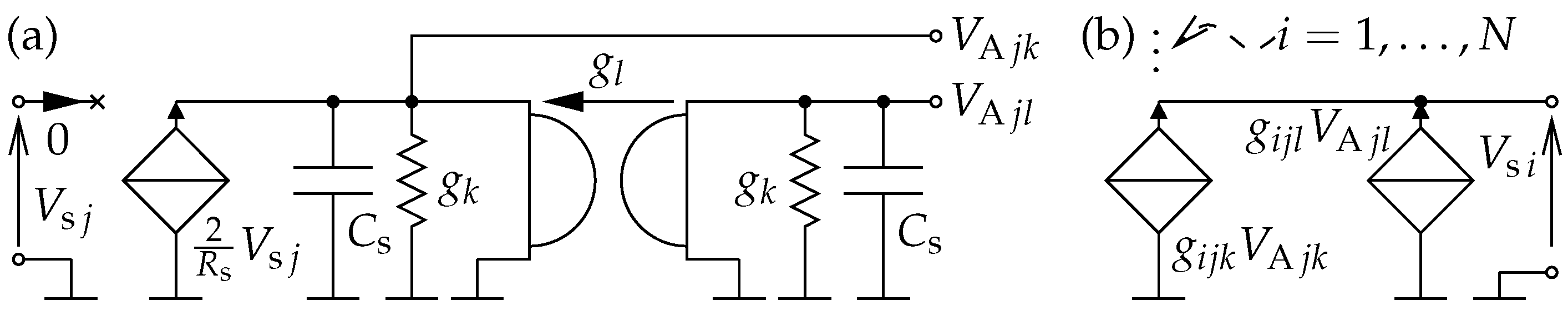
It may be beneficial to revisit the comparison of the current models and the previous author’s models described in [11] (see Figure 8). We had in [11], where and , so all model elements depend on the reference impedances. In the case of complex reference impedances, the computation of element values would require enormous effort. Contrary to this, in the present approach, and , so only the N outermost model elements depend on the reference impedances, where N is the number of ports. The remaining element values are given directly and do not require computations. As stated at the end of Section 2, if and only if the reference impedances of all ports are real and equal to will both the present and the previous author’s models be identical.

Figure 8.
A comparison of the present and the previous author’s models (the transforming two-port is expanded only for the i-th port).
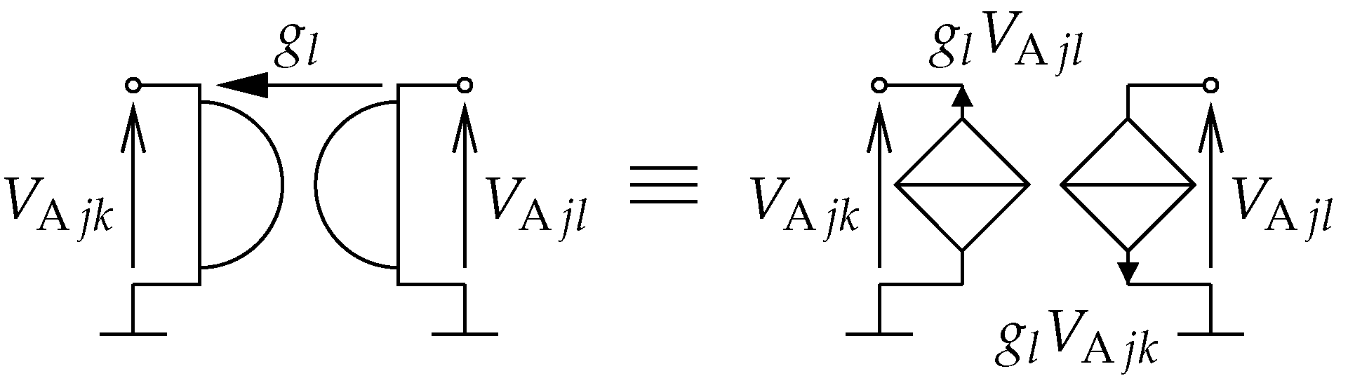
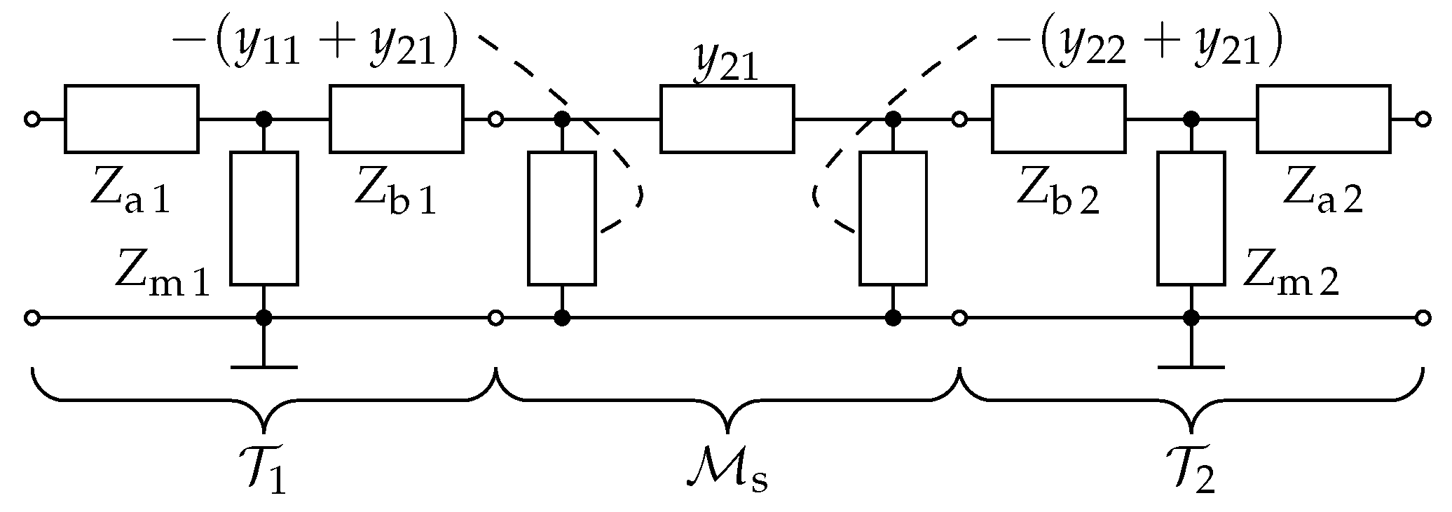
In numerous practical cases, two connected ports (e.g., the i-th and the j-th) of some system elements have identical reference impedances: . In such circumstances, the two corresponding transforming two-ports and are identical but have opposite orientations. They constitute a symmetric two-port as illustrated in the left part of Figure 9. The chain matrix of this two-port can be computed as the product of the inverse chain matrix of (which is not the inverse of its chain matrix) and the chain matrix of given by (12). This product equals:
and can easily be recognized as the chain matrix of a negative admittance inverter (NAV).
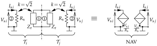
Figure 9.
A simplified model of the i-th and the j-th port interconnection for equal reference impedances : two cascaded transforming two-ports and are equivalent to a symmetric negative admittance inverter (NAV).
It should be noted that the above chain matrix (15) is independent of the reference impedance but depends only on the scaling resistance . Upon writing the chain equations corresponding to (15) and considering the definitions (1), one obtains the wave continuity conditions and as expected.
The NAV described by (15) can be realized as a simple three-element T- or -type two-port. However, using the model shown in the right part of Figure 9, which consists of two controlled sources, seems more convenient. This model guarantees the regularity of the connection of ports i and j and seems better suited for SPICE-like simulation programs based on the modified nodal approach.
4.2. Models for the Power Waves
In the case of power waves, the diamond symbol represents the complex conjugate operator. By multiplying the first equation in (4) by and the second by and then by adding both sides of the resulting formulas, we obtain the first equation in (16). On the other hand, by subtracting both sides of the equations in (4), we obtain the second equation in (16):
Subsequently, by inverting these relationships and recognizing that , we obtain:
Furthermore, by considering Equation (2), we finally obtain:
These are the chain equations of the transforming two-port . Its chain matrix is, therefore, equal to
and its determinant is given by
Once again, it is independent of the choice of the scaling resistance .
For the conventional definition of power waves (definition ), the determinant can be simplified to the form:
This form is identical to (10) presented in the preceding subsection. Thus, for the proportionality factor , the determinant will be equal to unity. In such a case, the transforming two-port chain matrix will equal:
Based on the chain matrix, the impedance and admittance matrix of the transforming two-port can also be determined:
and
In the case of power waves, the transforming two-port chain, impedance, and admittance matrices are more complicated than their counterparts for pseudo-waves. Nevertheless, the most straightforward implementation is based on the impedance matrix (23). It can be decomposed into the sum of two matrices:
corresponding to the series reactance (conjugated to the imaginary part of the reference impedance) next to the two coupled resistances (with the coupling coefficient again equal to the square root of two). One resistance is the real part of the reference impedance, and the other is the scaling resistance. The corresponding model is quite simple and is presented in Figure 10. These two coupled resistances can be implemented analogously to the impedance coupled to the resistance as discussed in the previous subsection. In the context of power waves, the reference impedance should be replaced by its real part in Figure 4, Figure 5, Figure 6 and Figure 7, including the formulas for mutual immitances and .
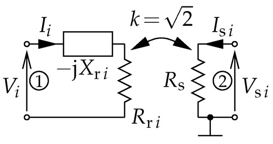
Figure 10.
A model of the transforming two-port for power waves, corresponding to the i-th port with the reference impedance , consisting of two coupled resistances with the coupling coefficient k and an uncoupled conjugated reference reactance.
5. Models of the Inner Multiport
Once the models of the transforming two-ports (for both pseudo-waves and power waves) have been defined, it is necessary to specify a model of the inner multiport .
5.1. Exact Models
According to (3), the inner multiport is described by its admittance matrix:
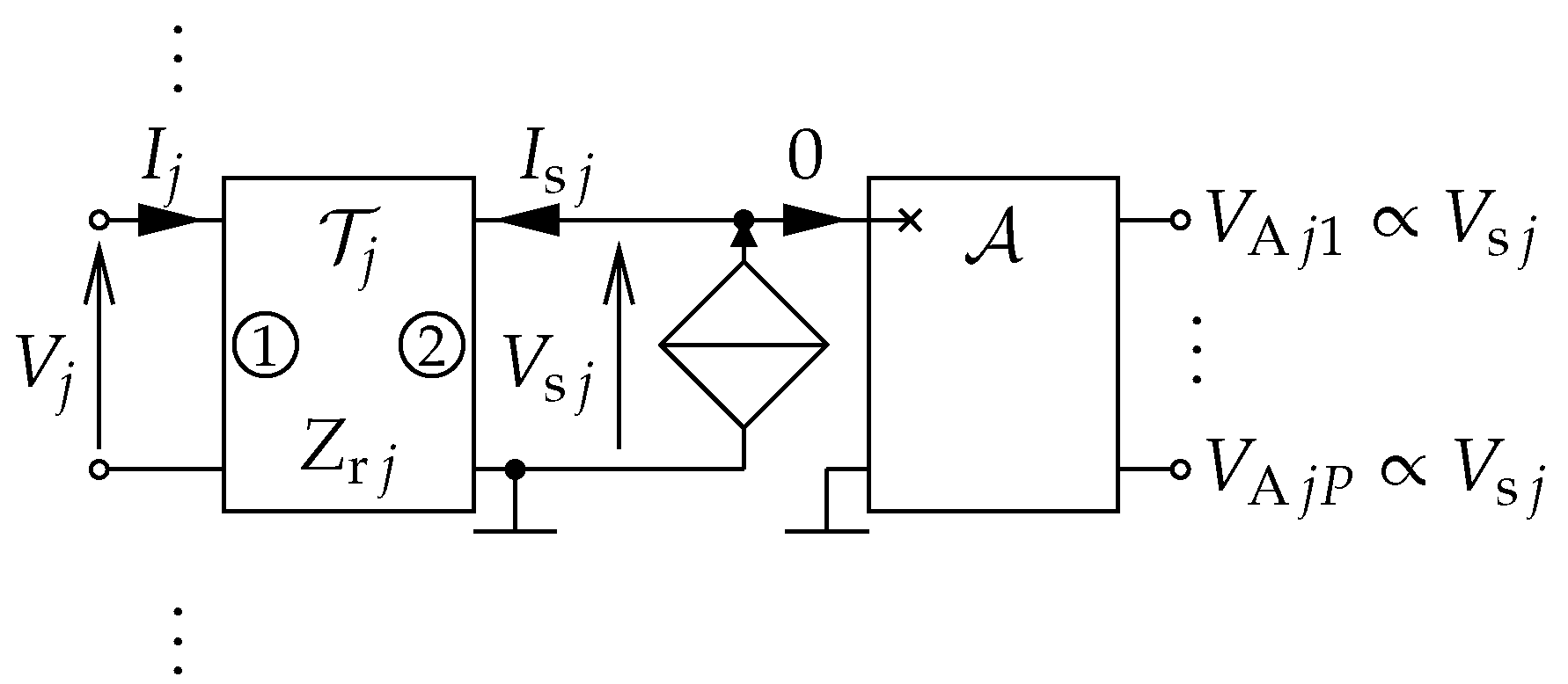
The most straightforward implementation well suited for the SPICE-like circuit simulators consists of a dependent current source at each i-th port, , with the current equal to:
The absence of a minus sign in (27) is due to the direction of the underlying current (see Figure 2). The part of such a model connected to the i-th port is shown in Figure 11. According to Equation (27), the voltage-controlled current source depends linearly on N voltages. In most simulation programs, such a source can be implemented as a parallel connection of N conventional dependent current sources controlled by a single voltage. Such a connection does not introduce any additional internal nodes to the model and, therefore, does not increase the size of the system matrix.
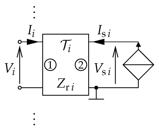
Figure 11.
An exact model of the N-port , which uses behavioral voltage-controlled current sources. Only the part connected to the i-th port is presented.
It should be emphasized that although the presented model is conceptually simple since the trans-admittances of the controlled sources for are numerically equal to the scattering parameters, the model parameters are frequency-dependent and usually provided in a tabular form. This fact necessitates the use of behavioral sources, which have two drawbacks:
- The generic SPICE program does not provide behavioral sources, so one has to resort to one of the modified SPICE versions. Some allow for the direct use of SnP or CITI files (e.g., in the HSPICE program via the TSTONEFILE or CITIFILE keywords, respectively). Others allow for the convenient inclusion of tabulated data (e.g., in the LTSPICE and PSPICE programs using the FREQ keyword and the .include directive).
- The analysis of circuits containing behavioral sources that use tabulated data is recognized as slow (see [29] and the timing data provided in Section 7 in the present paper.
As a final note concerning the exact behavioral models, let us consider the following modification of the author’s model presented above. Firstly, we will assume that all reference impedances are positive real: . Secondly, we will withdraw the assumption that the scaling resistance is globally defined for the whole multiport and instead define individual scaling resistances for each i-th port as . The chain matrix (12) of the transforming two-port (in the case of pseudo-waves) takes the form:
This matrix has a determinant equal to one. It can, therefore, be synthesized as a reciprocal circuit in the form of the inverted--type two-port, consisting of the series impedance followed by the shunt impedance . If we employ such a two-port in the model depicted in Figure 11 and then convert the parallel connection of the latter (shunt) impedance and the current source to the Thévenin equivalent, we will obtain the widely cited model presented in Figure 21 of [2]. This model, which is defined in [2] only for a two-port with equal reference impedances of both ports, contains a controlled voltage source with an electromotive force equal to , that can be implemented as a series connection of N conventional dependent voltage sources controlled by a single voltage. The advantage of voltage sources is that their coefficients are dimensionless, so they can be directly identified with the scattering parameters without resorting to the scaling resistance . However, the series connection of N voltage sources introduces extra internal nodes of the model (N sources for each of N ports), dramatically increasing the dimensions of the system matrix and, as a consequence, the analysis time. The experiments described in Section 7 of the present paper will confirm this observation.
In conclusion, the proposed exact model of the inner multiport does not introduce any internal model nodes and necessitates the use of behavioral voltage-controlled current sources.
5.2. Approximate Models
One potential reason for the extended analysis time of models incorporating behavioral sources defined by tabulated frequency-dependent parameters is the time required for table lookup and interpolation. To test this hypothesis, an investigation was conducted into approximate models, where the frequency dependence is defined in terms of the rational approximation of the tabulated data in the Laplace (s-variable) domain. Several SPICE program variants permit the description of behavioral sources in terms of the rational function in the s variable, using the LAPLACE keyword. In such instances, the number of terms in the partial fraction expansion of the rational approximation is typically fewer than the number of frequency points in the table.
It should be noted that the approximation of the matrix as a whole is required, i.e., functions of the Laplace variable s are needed. As a simplifying assumption, we will use the same denominator (and thus the same set of poles) for all functions. The elements of the approximated matrix will differ only by their numerators (or, equivalently, residues). This approach is widely employed as evidenced by the so-called MIMO structure in [30] or [31]. It arises from the fact that when converting any multiport matrix (e.g., chain, impedance and admittance) to the scattering matrix using formulas such as those in [32,33] or [34], one obtains a common denominator of all scattering parameters.
Among the various techniques for approximating a family of complex frequency functions in MIMO structure (e.g., see a comparison in [35]), the most prevalent is the vector-fitting method [30] (Chapter 7). The newly introduced AAA algorithm (adaptive Antoulas–Anderson) has recently garnered increasing interest. The free code for the MIMO version of the AAA algorithm can be downloaded from the repository pointed to in [36] (Footnote 1 in Section 4).
It is, therefore, assumed that the P poles , are common for all scattering parameters, with the residues individually assigned to each scattering parameter :
where is a direct term of the partial fraction expansion. Among these P poles, let there be real poles and pairs of complex conjugated poles: . Let the poles be ordered so that the complex conjugated pairs come first, and within the pair, the pole with the positive imaginary part comes first:
where
These conditions imply the ordering of the corresponding residues of the scattering parameter , for . Consequently, we obtain:
By inserting the approximation (29) into (27), we obtain:
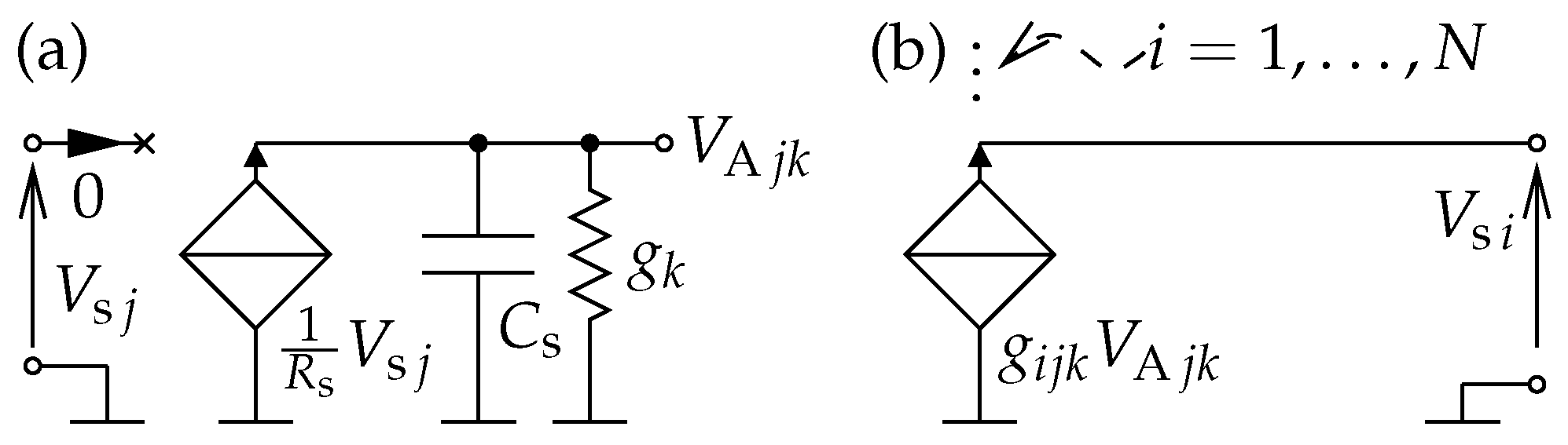
The form of this formula suggests the method of implementing it. Since in the MIMO structure, the denominators of the rational approximations of all scattering parameters are the same, the same grounded subcircuit should be created for each port. The role of this subcircuit is to sample the voltage without drawing any current and to generate a set of P proportional voltages corresponding to individual partial fractions (see Figure 12). To ensure that the circuit is identical for all ports, it is necessary to replace the partial fractions numerators (residues ) with simple constants of the appropriate physical dimension. Given that the poles and residues have the dimension of angular frequency [/] and that the trans-admittance of the controlled sources should be expressed in [], it is necessary to introduce a scaling capacitance , common to the entire modeled multiport , with a unit value (e.g., or , according to the desired frequency range). The dimensionless direct term should then be divided by the previously introduced scaling resistance . As the subcircuit is identical for all ports, it can be conveniently implemented as a macro-model (using the SPICE .subckt directive).
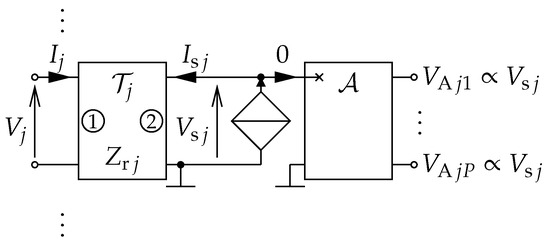
Figure 12.
Approximate (lumped) model of the N-port , which uses conventional voltage controlled current sources. Only the part connected to the j-th port is presented. Note that the -terminal subcircuit , responsible for the P poles of the rational approximation, is the same for all ports. Symbol ∝ means “proportional to”.
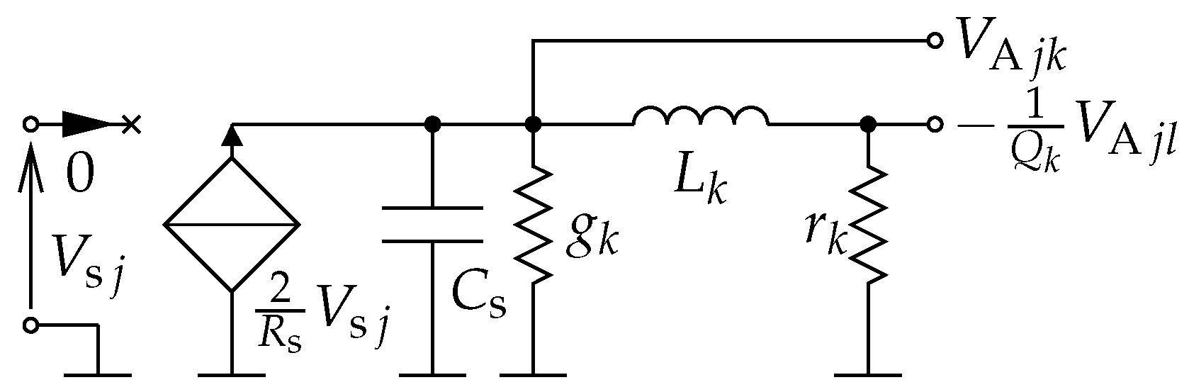
A scaled partial fraction in (33) corresponding to the single pole can be expressed in the form:
The first braced factor can be interpreted as a voltage transfer function of the two-port that is a part of the subcircuit connected to the j-th port. The implementation of the two-port is straightforward (see Figure 13a). The two-port retrieves the voltage with a dependent current source of the trans-admittance equal to , connected to the standard RC cell. The resistor utilized has the conductance as indicated in Table 2, which is positive for the pole on the left real semi-axis. The second braced factor in (34) represents a trans-admittance of the current source connected to the i-th port and controlled by the voltage (see Figure 13b).

Figure 13.
A part of the model responsible for the single real pole of the rational approximation (k-th pole). (a) A part of the subcircuit connected to the j-th port. (b) A controlled source responsible for the contribution of this pole from the j-th port to the i-th port.
In the case of a pair of complex conjugate poles, it is necessary to consider both corresponding partial fractions simultaneously. By taking into account (31) and (32), we obtain:
where . The first braced factor in both terms can be interpreted as the voltage transfer function or of the three-port that is a part of the subcircuit connected to the j-th port. The second braced factor in both terms is the trans-admittance or of the dependent current source connected to the i-th port and controlled by voltage . Implementing this three-port is more complex than before (see Figure 14). The comparison with the real-pole case reveals that the corresponding circuit has doubled the trans-admittance of the dependent source sampling the input voltage and duplicated RC cells coupled with a gyrator. The resistors utilized have the conductance as indicated in Table 2, which is positive for the poles in the left half plane. The formula for the gyration conductance is provided in Table 2 as well. Alternatively, one can reverse the gyration direction and the dependent source .
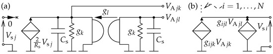
Figure 14.
A part of the model responsible for the complex conjugate pole pair of the rational approximation (k-th pole, with positive imaginary part, and l-th pole, where ). (a) A part of the subcircuit connected to the j-th port. (b) A set of the controlled sources corresponding to the contribution of this pole pair from the j-th port to the i-th port.
Following the replacement of the gyrator with a pair of controlled sources as illustrated in Figure 15, the circuits from Figure 13 and Figure 14 become very similar to models based on state equations in [30] (Figures 11.8 and 11.9) and [31] (the middle part of Figure 5). However, the approach proposed in this work is more suitable to the requirements set out in Section 1 and the specificity of the SPICE program due to the method of implementing the residues. In the book [30], the trans-admittances of controlled sources depend on the square roots of the reference impedances, so in the general case, they are complex and frequency-dependent. The article [31] employs trans-admittances dependent on the reference impedance and current-controlled current sources, which have more complicated SPICE models than those required by the author’s approach. In the present work, all current sources that implement residues are voltage-controlled, and their trans-conductances are constants independent of the reference impedance.
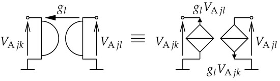
Figure 15.
A simple model of the gyrator used in the part of the subcircuit responsible for the complex conjugate pole pair of the rational approximation.
We elected to place a gyrator in the schematics presented in Figure 14 instead of a pair of controlled sources as in Figure 15, to illustrate an alternative implementation of a pair of conjugated complex poles. This alternative implementation is, in fact, primary to the one presented above. Namely, considering the impedance transformation by the gyrator (a positive-impedance inverter), the circuit shown in Figure 14 is equivalent (up to the rightmost node voltage scaling) to the circuit shown in Figure 16. The latter can be regarded as a parallel resonant circuit with lossy reactance elements exhibiting the same individual quality factors at the resonant frequency. In this case, Formula (35) becomes:
where
is a quality factor of the resonant circuit. The conductance remains unchanged. The inductance value is , and the resistance value is . As before, for the poles in the left half plane. Preliminary experiments have demonstrated that the model of Figure 16 yielded virtually identical analysis times to those for the model of Figure 14, although with marginally worse numerical errors. Therefore, it was not investigated in detail further.
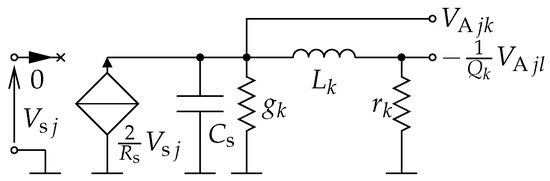
Figure 16.
An alternative realization of the part of the subcircuit connected to the j-th port, shown in Figure 14a. Note that the rightmost node voltage is scaled by the negated Q factor of the pole (defined as the absolute value of the ratio of the imaginary part to the real part).
The direct term has a straightforward implementation that does not require a figure. It is implemented as a single current source at the i-th port, controlled by the voltage of the j-th port, with transconductance equal to . In practice, this term appears rarely, as for many circuits, for high frequencies.
The insertion of (34) and (35) into (33) yields:
for . This formula and the accompanying Figure 12, Figure 13, Figure 14 and Figure 15 give insight into the complexity of the proposed approximate model of the inner multiport . Including the direct terms , the model introduces internal model nodes and requires resistors, capacitors, and conventional (not behavioral) voltage-controlled current sources with constant trans-admittances.
An analysis of Table 2 reveals that if the scaling capacitance is unity (such as ), all the (trans-)conductances are numerically equal to the real or imaginary part of the pole or residue. Consequently, the model element values directly relate to the partial fraction expansion, resulting in a simple model construction. However, it should be noted that the resistors in Figure 13 and Figure 14 are defined by their conductance , not resistance. SPICE does not feature conductances as primary elements. Consequently, one must numerically invert the conductance to provide the resistance , thereby destroying the direct relationship between the element values and partial fraction coefficients. Alternatively, it is possible to simulate the conductance as a dependent current source with transconductance , controlled by its self-voltage. However, in such a case, one must provide an extra dummy resistor of a huge resistance in parallel to each mentioned source to guarantee the direct current path to the corresponding inner model node (as SPICE requires).
5.3. Comparison of the Exact and Approximate Models
The procedure for utilizing the two kinds of models proposed in this paper is as follows: the measured or simulated scattering parameters serve as the input data for the simulation. With regard to the exact models, the tabularized scattering parameters serve as the element values of the behavioral voltage-controlled current sources. In the case of the approximate models, a rational approximation of the scattering parameters is performed, leading to a set of their poles and residues, which serve as the element values of the conventional voltage-controlled current sources. The generation of the model netlist can be expedited through the use of any convenient scripting language.
A brief comparison of the principal characteristics of the exact and approximate models is presented in Table 3. Note that the right column does not refer to the approximate model using behavioral sources via the LAPLACE keyword. Some of the statements are based on the results presented in Section 7 below.
Table 3.
Side-by-side comparison of exact and approximate models of the inner multiport.
6. Examples
6.1. One-Port—Arbitrary Impedance
As a preliminary example, consider a one-port element, which is a two-terminal device with impedance Z. The scattering parameter for this element is equal to the reflection coefficient: . The complete model of the impedance, presented in Figure 17, instead of a controlled source, contains an admittance equal to the scaled and negated scattering parameter. The coupled impedances in the transforming two-port are represented by the equivalent T-type connection of impedances with (see Figure 6).
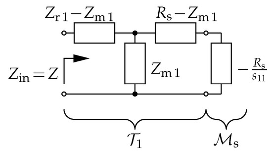
Figure 17.
Example 1. A model of the impedance Z treated as a one-port with the reference impedance . The T-type model of the transforming two-port was used (see Figure 6), with the ideal transformer removed due to the inherent regularity of any one-port connection to the rest of the circuit.
6.2. Two-Port—Described by Admittance Parameters
The second example concerns a grounded reciprocal two-port () with different reference impedances of the ports. The corresponding inner two-port can be realized as a -type connection of three admittances as shown in Figure 18, with element values equal to the summed up and negated scattering parameters. Hence, the scattering parameters are incorporated almost directly into the schematic. Two T-type transforming two-ports have , , and , .
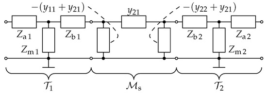
Figure 18.
Example 2. A model of the grounded reciprocal two-port, which is described by the admittance matrix. The T-type model of the transforming two-ports was used (see Figure 6), with the ideal transformers removed due to the grounding of both ports of the modeled two-port. Note that , and . For the inner two-port , element admittances are given.
6.3. Three-Port—Ideal Circulator
The third example presents a model of an ideal grounded circulator with just three non-zero scattering parameters, all equal to one. Once again, different reference impedances of its ports are assumed. Its model presented in Figure 19 contain conventional dependent current sources with trans-admittances equal to the reciprocal of the scaling resistance. All transforming two-ports have element values given by the same formulas as in the previous example.
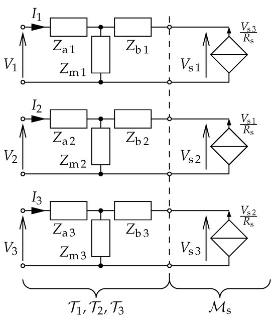
Figure 19.
Example 3. A model of the grounded three-port circulator. The T-type model of the transforming two-ports was used (see Figure 6), with the ideal transformers removed due to the grounding of all ports of the modeled circulator. Note that , and , .
6.4. Four-Port—Asymmetric Coupler (Real-World Problem)
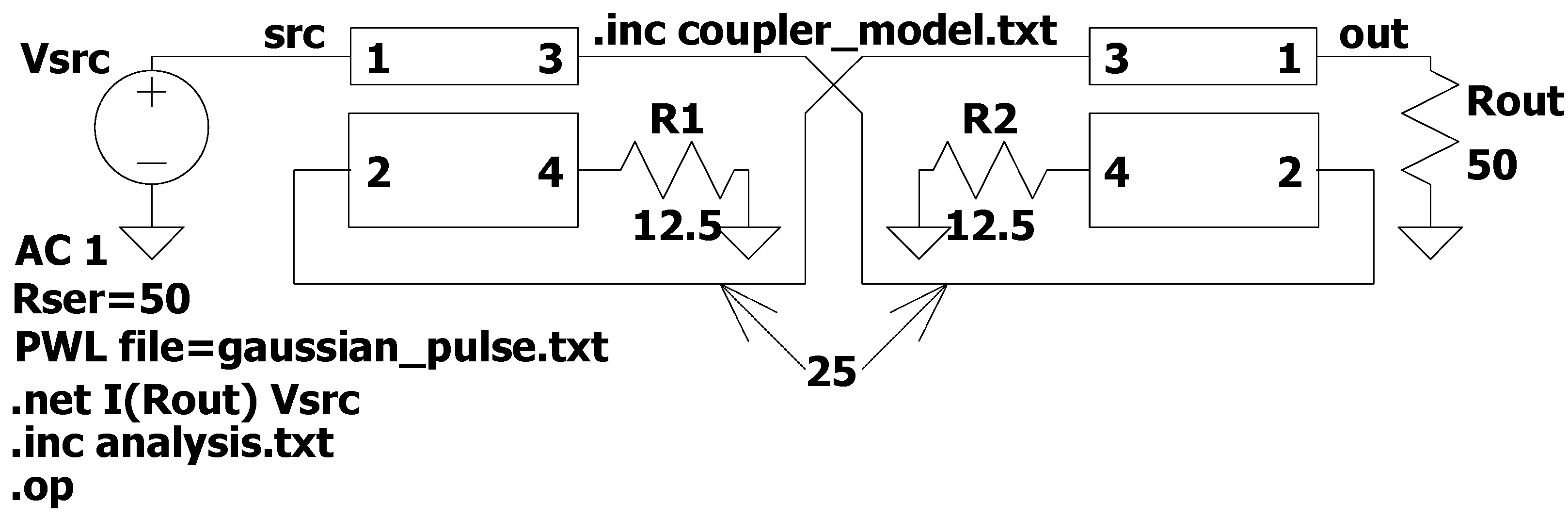
In contrast to the preceding, more academic, instances, the fourth example is a real-world one. It refers to a balanced circuit that consists of two identical directional couplers, presented in Figure 20. The circuit is taken from [37] (Figure 5 and Table I) but has a slightly modified microstrip layout. The couplers are asymmetric and thus can serve as impedance transformers, naturally featuring different reference impedances of each port ( at port 1, at ports 2 and 3, and at port 4).

Figure 20.
Example 4. An LTSPICE schematic of the balanced circuit consisting of two identical asymmetric directional couplers. Notice three different reference impedance levels (, , and ). The included file coupler_model.txt contains the LTSPICE model of the coupler; the analysis was performed for several different models, including the proposed ones and a few others mentioned in the literature (see Table 4). The included file analysis.txt defines the LTSPICE analysis type required, either frequency domain (.ac directive) or time domain (.tran directive).
7. Simulations
All simulations will be based on the fourth example presented in Section 6.4. The Advanced Design System (ADS) 2023 Update 2 was employed to compute and export to text files two independent S-parameters of the symmetric, balanced two-port (presented in Figure 20) and ten independent S parameters of the asymmetric coupler. The former parameters served as a reference solution, while the latter ones were used for the simulation as the parameters of the coupler model. The LTSPICE 17.0.37.0 program (Analog Devices Inc., Milpitas, CA, USA) was employed as a simulation engine for all numerical experiments. Six distinct coupler models were analyzed during these experiments: three were based on the existing commercial software and three were proposed in this work. The author’s models proposed in the present paper are A1, A2, and A3. The details of each model are presented in Table 4.
Table 4.
Models of the coupler used in numerical experiments.
Contrary to the examples from Section 6.1, Section 6.2 and Section 6.3, in models A1, A2, and A3, the -type transforming two-ports presented in Figure 7 were used, as they do not introduce any superfluous internal model nodes (in contrast to T-type two-ports). Ideal transformers were excluded, as the modeled couplers have all ports grounded. Furthermore, the simplified port interconnection models shown in Figure 9 were not utilized to maintain the coupler macro-model’s generic and autonomous nature.
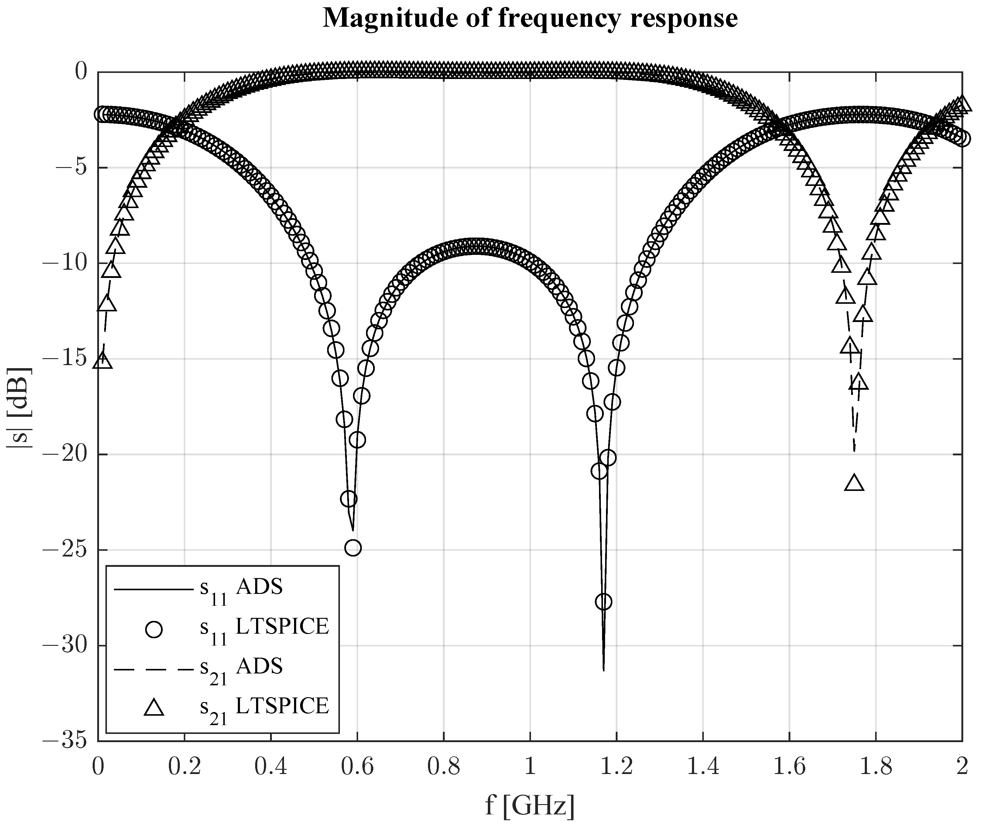
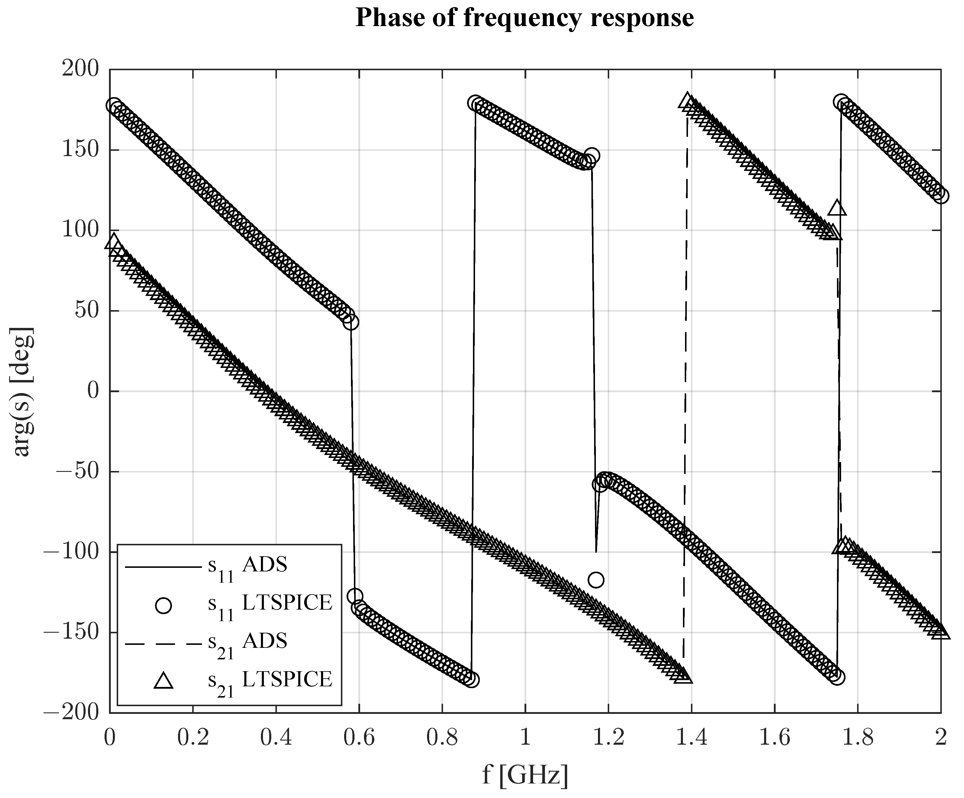
For both exact models, the simulated frequency characteristics in the range from to of the S parameters of the whole balanced two-port computed by LTSPICE were found to agree with the ADS reference solution up to the numerical noise, with the differences being as small as in magnitude and in phase. Furthermore, the absolute value of the difference between the simulated and reference parameters was found to be below within the analyzed frequency range. The simulation results, with differences (except for the proximity of the zeros) approximately in magnitude and 3° in phase, were as expected according to the presumed rational approximation accuracy. The absolute value of the difference between the simulated and reference parameters was below for all frequencies. It should be noted that the MATLAB model exhibits simulation errors that are about two times larger than those of other approximate models. This discrepancy can be attributed to the additional step required by MATLAB model, namely, the renormalization of scattering parameters of the couplers for , which also resulted in a different pattern of the poles. This is because the RF Toolbox in the version used (R2023b) does not allow for different reference impedances of the ports. The corresponding magnitude and phase characteristics are presented in Figure 21 and Figure 22, respectively. These results validate the models proposed in the present paper in the frequency domain.
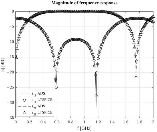
Figure 21.
Example 4. Results of the frequency-domain analysis of the circuit—the magnitude of the scattering parameters. LTSPICE results are presented as discrete points (circles or triangles), and the reference ADS simulation results as continuous or dashed lines.
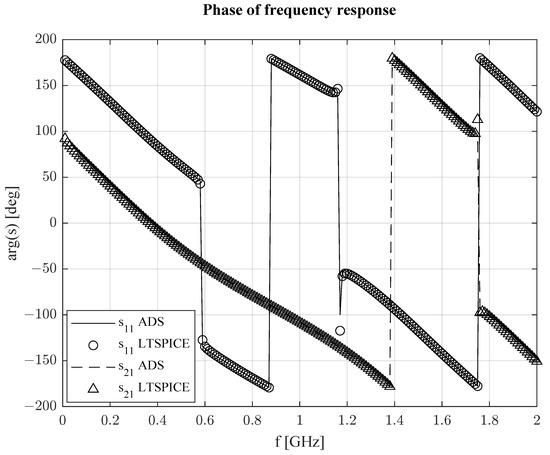
Figure 22.
Example 4. Results of the frequency-domain analysis of the circuit—the phase angle of the scattering parameters. LTSPICE results are presented as discrete points (circles or triangles), and the reference ADS simulation results as continuous or dashed lines.
Time-domain LTSPICE simulations were also performed for the input and output voltages (nodes labeled in Figure 20 as src and out, respectively) of the whole balanced two-port for all six models under investigation. The Gaussian pulse:
with a magnitude and a time-scale parameter was used as the excitation. Once more, the outcomes for all four approximate models were comparable to the reference ADS solution, with discrepancies of up to . The corresponding curves are plotted in Figure 23. However, both exact models (exact in the frequency domain) exhibited considerably inferior performance, resulting in up to of simulation errors. This could be attributed to the internal LTSPICE algorithms that translate the frequency-domain description to the time domain using the Discrete Fourier Transform. The manipulation of the transform parameters (number of FFT points and time window length) did not result in improved outcomes. This may be caused by the fact that the couplers under consideration have very low losses, which preclude them from meeting the requirement of having vanishing within the frequency range for which the scattering parameters are defined. Nevertheless, these results validate the models proposed in the present paper in the time domain.
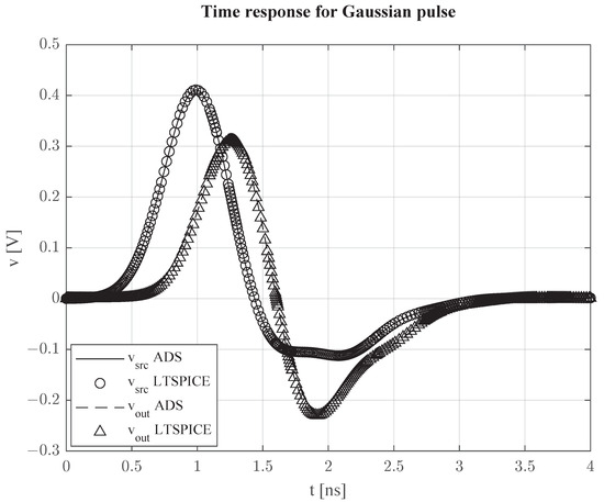
Figure 23.
Example 4. Results of the time-domain analysis of the circuit—plots of the input (src) and output (out) voltages. LTSPICE results are presented as discrete points (circles or triangles), and the reference ADS simulation results as continuous or dashed lines.
Furthermore, research has been conducted on the analysis time of all six models using the same environment: LTSPICE running under MS Windows 11 on a notebook computer equipped with an 11th Gen Intel Core i7-11800H processor running at . Given the variability in analysis time detected between consecutive LTSPICE runs of the same model, the minimal value observed across ten runs was taken as the result and is presented in Table 5 for the frequency-domain analyses (using different numbers of frequency points ranging from 2 to 20,000) and in Table 6 for the time-domain analyses. The tables also include two measures of the circuit complexity provided by LTSPICE: the system matrix size and the number of so-called fill-ins (i.e., the number of elements of the system matrix that changed from zero to non-zero during LU factorization). As anticipated, the matrix size was consistent across frequency- and time-domain analyses, but the number of fill-ins differed.
Table 5.
Example 4. Timing of the frequency-domain analysis of the circuit, using LTSPICE as the computing engine, for different models of the coupler.
Table 6.
Example 4. Timing of the time-domain analysis of the circuit, using LTSPICE as the computing engine, for different models of the coupler.
The results presented in Table 5 and Table 6 demonstrate that the author’s model A1 features the smallest matrix size and the lowest number of fill-ins among exact models (which inherently utilize behavioral dependent sources). Additionally, the author’s model A3 has the same advantages in the class of approximate models that utilize conventional dependent sources. While the author’s model A2 has the same low matrix size and the number of fill-ins as model A1, it results in unacceptably significant analysis times. Conversely, the author’s A1 and A3 models are faster than competitive solutions. However, the advantage of A3 over HFSS model in the time domain is marginal.
In order to gain a deeper understanding of the enhanced efficiency of the proposed models in relation to other solutions, a comparison of the required number of model elements of different types and the number of internal nodes introduced by the models is presented in Table 7. The number of internal nodes directly influences the system matrix size, which is a primary factor in the model’s efficiency. The number and type of elements determine the analysis time for a similar matrix size. Two simplifying assumptions were made during the construction of the table. Firstly, it was assumed that all ports were grounded. Secondly, it was assumed that reference impedances were real. The upper part of the table contains behavioral models (all but A2 are exact), while the lower part contains conventional approximate models.
Table 7.
Comparison of the number of the internal model nodes and of the number of various model elements for different models.
8. Conclusions
This paper proposes new circuit models of a multiport described by scattering parameters with reference impedances that are possibly complex and different for each port. The proposed exact models require behavioral sources, which are available in some versions of the SPICE program. The proposed approximate (lumped) models, based on the rational approximation of the scattering parameters, do not require behavioral sources and can be analyzed using generic versions of the SPICE program. Both categories of models can be utilized for a frequency-domain simulation at multiple frequency points and a time-domain simulation of mixed-mode networks, which contain elements described by circuit variables (voltages and currents) which can be non-linear, and linear elements described by scattering parameters. The exact model element values, dependent on the scattering parameters, are numerically equal to these parameters due to the appropriate scaling resistance. This enables the almost direct inclusion of text files that contain tabulated scattering parameters obtained from microwave simulators or network analyzers into the circuit description files. On the other hand, the approximate model element values are numerically equal to the real or imaginary part of the poles and residues of the rational approximation due to the proper choice of the scaling capacitance. These features of the exact and approximate models proposed in this paper simplify their practical applications, particularly when compared to numerous alternative approaches detailed in the literature [2,13,29,38,39,40,41,42,43,44,45,46,47,48,49,50]. Finally, a comparison was conducted using a common simulation environment based on the LTSPICE program, which demonstrated that the proposed models A1 and A3 exhibited the lowest matrix size, the lowest number of fill-ins, and the shortest analysis time among several popular competitive solutions. We direct the reader’s attention to Table 8 for a more detailed comparison between the proposed models and their counterparts.
Table 8.
Side-by-side comparison of the features of the proposed and existing models.
Funding
This research received no external funding.
Data Availability Statement
The data presented in this study are available in this article.
Acknowledgments
The author would like to express his sincere gratitude to Arkadiusz Lewandowski for providing the files with the tables of simulated scattering parameters used in Section 7 of this paper and for performing the reference ADS and HFSS analyses. The author would also like to thank the anonymous reviewers for their insightful comments and suggestions, which have contributed to the enhancement of the paper’s quality.
Conflicts of Interest
The author declares no conflicts of interest.
Abbreviations
The following abbreviations are used in this manuscript:
| NIV | negative impedance inverter |
| NAV | negative admittance inverter |
| MIMO | multi-input multi-output |
References
- Synopsys. HSPICE Signal Integrity User Guide; Synopsys: Mountain View, CA, USA, 2013; Version X-2005.09. [Google Scholar]
- Gerig, J.S. Create S-parameter subcircuits for microwave and RF applications. In MicroSim Application Notes, Version 8.0; MicroSim Corporation: Irvine, CA, USA, 1997; pp. 57–69. [Google Scholar]
- Iranzo, S. s2spice.c—A Program to Create a Pspice Model from Maxwell Eminence Results. Available online: https://www.eevblog.com/forum/rf-microwave/nanovna-custom-software/?action=dlattach;attach=818577 (accessed on 24 April 2024).
- ANSYS, Inc. Ansys Electromagnetics Suite 2022 R2. Ansys HFSS, Help System. Available online: https://www.ansys.com/Products/Electronics/ANSYS-HFSS (accessed on 24 April 2024).
- The MathWorks Inc. RF Toolbox Version: 23.2 (R2023b). Available online: https://www.mathworks.com/help/rf (accessed on 24 April 2024).
- Arsenovic, A.; Hillairet, J.; Anderson, J.; Forsten, H.; Ries, V.; Eller, M.; Sauber, N.; Weikle, R.; Barnhart, W.; Forstmayr, F. scikit-rf: An open source Python package for microwave network creation, analysis, and calibration [Speaker’s Corner]. IEEE Microw. Mag. 2022, 23, 98–105. [Google Scholar] [CrossRef]
- Amakawa, S. Scattered reflections on scattering parameters—Demystifying complex-referenced S parameters. IEICE Trans. Electron. 2016, E99.C, 1100–1112. [Google Scholar] [CrossRef]
- Kurokawa, K. Power waves and the scattering matrix. IEEE Trans. Microw. Theory Tech. 1965, 13, 194–202. [Google Scholar] [CrossRef]
- Tippet, J.C.; Speciale, R.A. A rigorous technique for measuring the scattering matrix of a multiport device with a 2-port network analyzer. IEEE Trans. Microw. Theory Tech. 1982, 30, 661–666. [Google Scholar] [CrossRef]
- Van Lil, E. Comments on “A rigorous technique for measuring the scattering matrix of a multiport device with a two-port network analyzer”. IEEE Trans. Microw. Theory Tech. 1985, 33, 286–287. [Google Scholar] [CrossRef]
- Nałęcz, M. Circuit models of multi-ports based on S-parameters with arbitrary reference impedances. In Proceedings of the EUROCON 2015—International Conference on Computer as a Tool, Salamanca, Spain, 8–11 September 2015; pp. 1–6. [Google Scholar] [CrossRef]
- Engelhardt, M. SPICE differentiation. Electron. World 2015, 121, 16–21. [Google Scholar]
- Quint, D.; Bois, K. The digital designer’s complete lossy transmission line model. In Proceedings of the 52nd Electronic Components and Technology Conference, San Diego, CA, USA, 28–31 May 2002; pp. 1073–1079. [Google Scholar] [CrossRef]
- Negri, S.; Spadacini, G.; Grassi, F.; Pignari, S. Measurement-based equivalent circuit model for time-domain simulation of EMI filters. In Proceedings of the 2022 International Symposium on Electromagnetic Compatibility—EMC Europe, Gothenburg, Sweden, 5–8 September 2022; pp. 793–798. [Google Scholar] [CrossRef]
- Youla, D.C. On scattering matrices normalized to complex port numbers. Proc. IRE 1961, 49, 1221. [Google Scholar] [CrossRef]
- Rahola, J. Power waves and conjugate matching. IEEE Trans. Circuits Syst. II Express Briefs 2008, 55, 92–96. [Google Scholar] [CrossRef]
- Hirano, T. Review and another derivation of the power wave. Microw. Opt. Technol. Lett. 2015, 57, 26–28. [Google Scholar] [CrossRef]
- Marks, R.B.; Williams, D.F. A general waveguide circuit theory. J. Res. Natl. Inst. Stand. Technol. 1992, 97, 533–562. [Google Scholar] [CrossRef]
- Williams, D.F. Traveling waves and power waves: Building a solid foundation for microwave circuit theory. IEEE Microw. Mag. 2013, 14, 38–45. [Google Scholar] [CrossRef]
- Muller, A.A.; Soto, P.; Moldoveanu, A.; Asavei, V.; Boria, V.E. A visual comparison between voltage and power wave reflection coefficients of microwave circuits. In Proceedings of the 2012 Asia-Pacific Microwave Conference Proceedings (APMC), Kaohsiung, Taiwan, 4–7 December 2012; IEEE: Piscataway, NJ, USA, 2012; pp. 1259–1261. [Google Scholar] [CrossRef]
- Llorente-Romano, S.; Garca-Lampérez, A.; Sarkar, T.K.; Salazar-Palma, M. An exposition on the choice of the proper S parameters in characterizing devices including transmission lines with complex reference impedances and a general methodology for computing them. IEEE Antennas Propag. Mag. 2013, 55, 94–112. [Google Scholar] [CrossRef]
- Pupalaikis, P.J. S-Parameters for Signal Integrity; Cambridge University Press: Cambridge, UK, 2020. [Google Scholar] [CrossRef]
- Pozar, D.M. Microwave Engineering, 4th ed.; John Wiley & Sons, Inc.: Hoboken, NJ, USA, 2012. [Google Scholar]
- Gwarek, W.K.; Celuch-Marcysiak, M. A generalized approach to wide-band S-parameter extraction from FD-TD simulations applicable to evanescent modes in inhomogeneous guides. In Proceedings of the 2001 IEEE MTT-S International Microwave Symposium Digest (Cat. No.01CH37157), Phoenix, AZ, USA, 20–24 May 2001; MWSYM-01. Volume 2, pp. 885–888. [Google Scholar] [CrossRef]
- Gwarek, W.K.; Celuch-Marcysiak, M. Wide-band S-parameter extraction from FD-TD simulations for propagating and evanescent modes in inhomogeneous guides. IEEE Trans. Microw. Theory Tech. 2003, 51, 1920–1928. [Google Scholar] [CrossRef]
- Zhu, L. Guided-wave characteristics of periodic coplanar waveguides with inductive loading – unit-length transmission parameters. IEEE Trans. Microw. Theory Tech. 2003, 51, 2133–2138. [Google Scholar] [CrossRef]
- Yu, S.; Petranovic, D.M.; Krishnan, S.; Kwyro, L.; Yang, C.Y. Loop-based inductance extraction and modeling for multiconductor on-chip interconnects. IEEE Trans. Electron Devices 2006, 53, 135–145. [Google Scholar] [CrossRef]
- Rübner-Petersen, T. NAP2: A Nonlinear Analysis Program for Electronic Circuits, Version 2, Users Manual 16/5-73; Report IT-63; Danmarks Tekniske Højskole, Instituttet for Teleteknik, Technical University of Denmark: Lyngby, Denmark, 1981. [Google Scholar]
- De Geest, J.; Sercu, S.; Clewell, C.; Nadolny, J. Making S-parameter data suitable for SPICE modeling. In Proceedings of the IEC DesignCon2004, Santa Clara, USA, 2–5 February 2004; pp. 1–23. [Google Scholar]
- Grivet-Talocia, S.; Gustavsen, B. Passive Macromodeling: Theory and Applications; Wiley: Hoboken, NJ, USA, 2015. [Google Scholar] [CrossRef]
- Chou, C.C.; Schutt-Ainé, J.E. Equivalent circuit synthesis of multiport S parameters in pole-residue form. IEEE Trans. Components Packag. Manuf. Technol. 2021, 11, 1971–1979. [Google Scholar] [CrossRef]
- Frickey, D.A. Conversions between S, Z, Y, h, ABCD, and T parameters which are valid for complex source and load impedances. IEEE Trans. Microw. Theory Tech. 1994, 42, 205–211. [Google Scholar] [CrossRef]
- Jarry, P.; Beneat, J. Advanced Design Techniques and Realizations of Microwave and RF Filters; Wiley: Hoboken, NJ, USA, 2007. [Google Scholar] [CrossRef]
- Freeman, J.C. On the Interpretation of Scattering Parameters. NASA Technical Reports Server. Available online: https://ntrs.nasa.gov/citations/20000056853 (accessed on 5 June 2024).
- Ma, A.; Engin, A.E. Orthogonal rational approximation of transfer functions for high-frequency circuits. Int. J. Circuit Theory Appl. 2022, 51, 1007–1019. [Google Scholar] [CrossRef]
- Lietaert, P.; Meerbergen, K.; Pérez, J.; Vandereycken, B. Automatic rational approximation and linearization of nonlinear eigenvalue problems. Ima J. Numer. Anal. 2021, 42, 1087–1115. [Google Scholar] [CrossRef]
- Wincza, K.; Gruszczyński, S. Asymmetric coupled-line directional couplers as impedance transformers in balanced and n-way power amplifiers. IEEE Trans. Microw. Theory Tech. 2011, 59, 1803–1810. [Google Scholar] [CrossRef]
- Vakanas, L.P.; Cangellaris, A.C.; Palusiński, O.A. Scattering parameter-based simulation of transients in lossy nonlinearly terminated packaging interconnections. IEEE Trans. Components Packag. Manuf. Technol. Part B 1994, 17, 472–479. [Google Scholar] [CrossRef]
- Troyanovsky, B.; Chang, N.; Dowell, D. Integration of Transient S-Parameter Simulation into HPSPICE; Technical Report, HPL-95-61; HP Laboratories: Palo Alto, CA, USA, 1995. [Google Scholar]
- Divekar, D.; Raghuram, R.; Wang, P. Automatic generation of Spice macromodels from N-port parameters. In Proceedings of the 37th Midwest Symposium on Circuits and Systems, Lafayette, LA, USA, 3–5 August 1994; MWSCAS-94. IEEE: Piscataway, NJ, USA, 1994; Volume 1, pp. 670–673. [Google Scholar] [CrossRef]
- Steenput, E. A Spice Circuit Can Be Synthesised with a Specified Set of S-Parameters. Ph.D. Thesis, Department ELEC, Vrije Universiteit Brussel, Brussel, Belgium, 1999. [Google Scholar]
- Timmermann, C.C. Exact S-parameter models boost SPICE. IEEE Circuits Devices Mag. 1995, 11, 17–22. [Google Scholar] [CrossRef]
- Gómez, J.M.; Alonso, J.I. A new approach for the extraction of SPICE compatible models from measured parameters of microwave circuits. In Proceedings of the IEEE MTT-S International Microwave Symposium Digest, Baltimore, MD, USA, 7–12 June 1998; MWSYM-98. IEEE: Piscataway, NJ, USA, 1998; Volume 1, pp. 275–278. [Google Scholar] [CrossRef]
- Gómez, J.M.; Alonso, J.I. A new technique for incorporating microwave circuits into SPICE from S parameters data. In Proceedings of the 28th European Microwave Conference, Amsterdam, The Netherlands, 5–9 October 1998; IEEE: Piscataway, NJ, USA, 1998; Volume 2, pp. 237–242. [Google Scholar] [CrossRef]
- Gómez, J.M.; Alonso, J.I. Making a better interconnection through modeling. IEEE Circuits Devices Mag. 1999, 15, 24–32. [Google Scholar] [CrossRef]
- Neumayer, R.; Haslinger, F.; Stelzer, A.; Weigel, R. Synthesis of SPICE-compatible broadband electrical models from n-port scattering parameter data. In Proceedings of the IEEE International Symposium on Electromagnetic Compatibility (EMC), Minneapolis, MN, USA, 19–23 August 2002; Volume 1, pp. 469–474. [Google Scholar] [CrossRef]
- Schutt-Ainé, J. Robust SPICE circuit generation using scattering parameters. In Proceedings of the IEEE International Symposium on Electromagnetic Compatibility (EMC), Raleigh, NC, USA, 4–8 August 2014; IEEE: Piscataway, NJ, USA, 2014; pp. 230–233. [Google Scholar] [CrossRef]
- Schutt-Ainé, J. SPICE circuit synthesis from complex pole-residue S-parameter representation. In Proceedings of the 2016 Asia-Pacific International Symposium on Electromagnetic Compatibility (APEMC), Shenzhen, China, 17–21 May 2016; pp. 1050–1052. [Google Scholar] [CrossRef]
- Heyfitch, V.; Dmitriev-Zdorov, V.; Pratt, G.L.; Azgomi, S. Fast Time-Domain Simulation of 200+ Port S-Parameter Package Models. 2006. In Proceedings of the DesignCon 2006, Santa Clara, CA, USA, 6–9 February 2006. [Google Scholar]
- Tseng, W.L.; Lee, C.H.; Li, S.C.; Pai, Y.C.; Hsu, S.K. Equivalent Circuit Simulation System and Method for HSPICE. U.S. Patent 8,489,379 B2, 16 July 2013. [Google Scholar]


Disclaimer/Publisher’s Note: The statements, opinions and data contained in all publications are solely those of the individual author(s) and contributor(s) and not of MDPI and/or the editor(s). MDPI and/or the editor(s) disclaim responsibility for any injury to people or property resulting from any ideas, methods, instructions or products referred to in the content. |
© 2024 by the author. Licensee MDPI, Basel, Switzerland. This article is an open access article distributed under the terms and conditions of the Creative Commons Attribution (CC BY) license (https://creativecommons.org/licenses/by/4.0/).