Abstract
This paper presents a novel multiple-input and multiple-output current-mode universal analog filter with electronic tuning capability. The proposed circuit uses a single second-generation current-controlled current conveyor with extra-X terminals (EX-CCCII) and two grounded capacitors. The filter can offer five standard filtering functions, namely low-pass, high-pass, band-pass, band-stop, all-pass responses, in the same circuit without changing the internal configuration of the filter by selecting appropriate input and output signals. To obtain the five standard filtering functions, inverted input signal and input matching conditions are absent. The natural frequency of all filter responses can be electronically controlled. The proposed circuit was simulated by SPICE using 0.18 μm CMOS process from Taiwan Semiconductor Manufacturing Company (TSMC). The results of experiments using the integrated circuit operational amplifier AD844 confirm the functionality of the new filter.
1. Introduction
In many circuit designs, a second-generation current conveyor (CCII) is utilized to realize analog signal processing circuits, especially current-mode signal processing circuits. The circuits using CCII as an active element offer higher linearity, better signal bandwidth, and wider dynamic range compared to the operational amplifier (op-amp) based circuits [1,2]. Moreover, CCII is simpler to implement compared to the op-amp structure. There are many CCII structures available in literature [3,4,5,6,7,8,9,10,11,12,13,14,15]. In [3], a conventional CCII that has three terminals (the y-, x-, z-terminals) is proposed. This CCII provides the characteristics of Vy = Vx, Ix = Iz, a high resistance at the y- and z-terminals (ideally infinite), and a low resistance at the x-terminal (ideally zero). In practice, however, the resistance at the x-terminal is not equal to zero as it exhibits a parasitic resistance. In [4], a current-controlled CCII (CCCII) is introduced. Due to the CCCII, the parasitic resistance at the x-terminal (Rx) can be used as a parameter for filter application and this Rx can be electronically controlled. Moreover, the CCCII-based circuit does not contain a passive resistor. Note that the CCCII still has a single x-terminal, like the CCII.
Recently, the extra x-terminal CCII (EX-CCII) has been introduced [5]. This device is an enhancement of the conventional CCII, which increases the number of x- and z-terminals.
Figure 1 shows the electrical symbol of the conventional CCII and the EX-CCII. Compared with the conventional CCII in Figure 1a, the EX-CCII in Figure 1b has extra x-input terminals and z-output terminals. The characteristics of the EX-CCII can be given by Vy = Vx1 = Vx2, Ix1 = Iz1, and Ix2 = Iz2. In addition, the number of x-input terminals and z-output terminals of the EX-CCII can be increased to any number. Thus, the EX-CCII is a versatile and flexible active device. There are many applications of the EX-CCII available in literature, including precision rectifiers [6,7,8,9], fractional-order controllers [10,11,12], digital modulators [13], analog multipliers [14], wave signal generators [15], first-order filters [16,17], and universal filters [18]. It is worth noting that the EX-CCII based circuit does not provide electronic tuning capability.
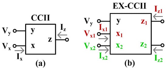
Figure 1.
Electrical symbol of (a) a conventional CCII and (b) an EX-CCII.
If the parasitic resistance at the x-terminal of the EX-CCII is considered, then the circuit becomes EX-CCCII and its parasitic resistances at the x-terminals can be used as an adjustable parameter. This is advantageous for applications such active filters and oscillators. The EX-CCCII can be used for applications such as oscillators [19,20,21,22,23], instrumentation amplifiers [24,25], immittance simulators [26], precision rectifiers [27], first-order filters [28,29,30], and universal filters [31,32,33,34]. This work focuses on the EX-CCCII based universal filter. Considering the universal filters in [31,32,33,34], these filters suffer from some drawbacks. First, in order to obtain the five filtering functions (i.e., the low-pass filter (LPF), high-pass filter (HPF), band-pass filter (BPF), band-stop filter (BSF), and all-pass filter (APF)), the filters use inverted input signals and require input matching condition [31,32,33,34]. Second, the filters use passive component matching conditions [34]. The use of a single EX-CCCII based filter, made possible through the use of the current-mode technique, is advantageous in these universal filters [31,32,33,34]. Note that the realization of signal addition and subtraction in current-mode circuits is easier than for their voltage-mode counterparts.
This work proposes a single EX-CCCII-based current-mode universal filter. It is a multiple-input and multiple-output filter providing five standard filtering functions, namely low-pass, high-pass, band-pass, band-stop, and all-pass functions, that can be obtained by selecting appropriate input and output terminals. The proposed filter offers the following advantages: (i) it uses a single EX-CCCII; (ii) it does not require inverted input signals or the fulfilment of input matching conditions to realize the five standard filtering functions; (iii) it does not require matching of passive components; (iv) it offers electronic tuning capability of a natural frequency.
2. Circuit Description
This section contains four subsections, where the first subsection introduces the second generation current-controlled current conveyor with extra-x terminal that is used for realizing the proposed filter. The second subsection introduces the proposed current-mode universal filter, while the non-ideal gain analysis and non-ideal parasitic analysis are presented in the third and fourth subsections, respectively.
2.1. Second-Generation Current-Controlled Current Conveyor with Extra-X Terminal
Figure 2a shows the electrical symbol of the EX-CCCII and Figure 2b shows the equivalent circuit. The input voltage present at the y-terminal is conveyed to the x1- and x2-terminals. Rx1 and Rx2 are the parasitic resistances at the x1- and x2-terminals, respectively, that can be controlled by the DC biasing current.
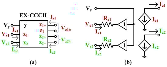
Figure 2.
EX-CCCII (a) electrical symbol, (b) equivalent circuit.
The input current at the x1- and x2-terminals is conveyed to the z1- and z2-terminals, respectively. The minus-type output of the z1- and z2-terminals can easily be obtained using a cross-coupled current mirror topology. Thus, the port relationships of the ideal EX-CCCII shown in Figure 2a can be given by
The CMOS structure of the EX-CCCII in Figure 2a is shown in Figure 3. The circuit is based on complementary source followers, current mirrors, and cross coupled current mirrors. The complementary source follower is a dual translinear loop (M1, M2, M4, M5) and (M1, M3, M4, M6) where the gate-source voltages VGS of the NMOS transistors (M1, M2 and M3) and PMOS transistors (M4, M5 and M6) are to match. In these loops, the input voltage is transferred to the outputs of the follower and precisely; if the drain currents of M1, M4 equal to the drain currents of M2, M5 and M3, M6 and vice versa, the drain current of M1, M4 is transferred precisely to M2, M5 and M3, M6 if the input and output voltages and the gate-source voltages of the respective transistors and their size are equal. The current mirrors (M9, M10, M14, M15, M21, M22, M26, M27) are used to transfer the x terminals current to their respective z+ terminals. The cross coupled current mirrors (M11–M13, M16–M18, M23–M25, M28–M30) are used to transfer the x+ terminals current to their respective negative z- terminals. The biasing circuit realized by the transistors Mb, M7, M8, M19, M20 and the biasing current source Iset provides all reference currents in the circuit.
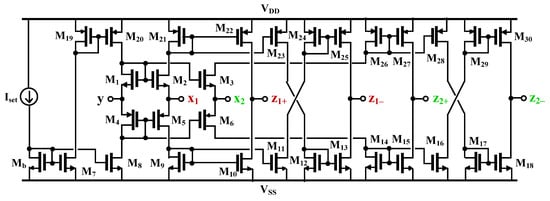
Figure 3.
CMOS structure of EX-CCCII.
Considering a dual translinear loop, the parasitic resistances Rx1 and Rx2 at the x1- and x2-terminals, respectively, can be expressed [32] by
where Iset is the biasing current, Cox is the oxide capacitance per unit area, and are the mobility of the holes and electrons, respectively, (W/L)p is the ratio of width to length of the channels of M5–M6, and (W/L)n is the ratio of width to length of the channels of M2–M3. From (2), the parasitic resistances Rx1 and Rx2 can be controlled by the biasing current Iset. These resistors have the same resistance values.
The input current at the x1-terminal is conveyed to the z1+-terminal by the current mirrors M7–M8, M19–M20, and the input current at x2 is conveyed to z2+ by the current mirrors M12–M13, M24–M24. The minus-type outputs z1− and z2− can be implemented using the cross-coupled current mirror topology. Additional copies of these z+,− outputs can be obtained using the cascade structure for these terminals.
2.2. Current-Mode Universal Filter Using EX-CCCII
Figure 4a shows the proposed current-mode universal filter, and the block diagram that corresponds to Figure 4a is shown in Figure 4b. It is based on one lossless integrator and one lossy integrator loop. It employs one EX-CCCII and two grounded capacitors. Thanks to the extra x-terminal and multiple-outputs of the EX-CCCII, the filter is realized with only one active block. The circuit has four input currents (I1, I2, I3, I4) and three output currents (Io1, Io2, Io3). Using (1) and nodal analysis, the outputs of the circuit in Figure 4a is given by
where .
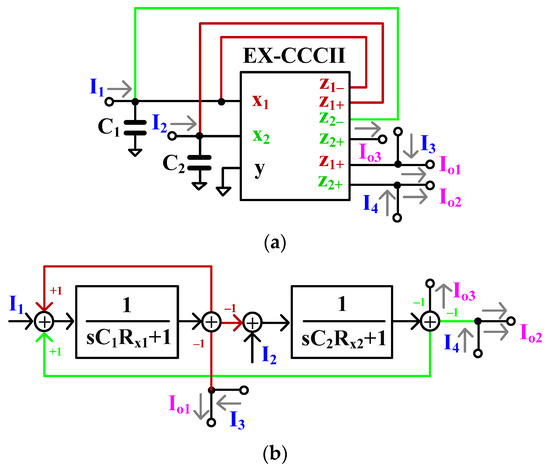
Figure 4.
(a) Proposed current-mode universal filter using EX-CCCII, (b) its block diagram.
From (3)–(5), the variant filtering functions of the low-pass filter (LPF), high-pass filter (HPF), band-pass filter (BPF), band-stop filter (BSF), and all-pass filter (APF) can be obtained, as shown in Table 1. For Table 1, it should be noted that the input terminal that is not selected to supply input signals can be floating, while the output terminal that is not selected to supply output signals should be grounded.

Table 1.
Variant filtering functions.
The natural frequency () and the quality factor () of all filter responses are given by
From Table 1, it is evident that the circuit does not need an inverted input signal, i.e., Iin, and double input signal, i.e., 2Iin, to realize all filtering functions.
From (6), we can see that the natural frequency can be controlled electronically by and through the biasing current Iset. The quality factor, as shown in (7), is given by while maintaining = .
2.3. Non-Ideal Gain Analysis
Taking the errors of the EX-CCCII into account, the relationship of the terminal voltages and currents can be written by
where is the voltage gain from y-terminal to -terminal, and is the current gain from -terminals to -terminals ( = 1, 2). Ideally, and should be equal to 1. However, in practice, these unity gains will be affected by the voltage and current tracking errors. These can be expressed by and , where is the voltage tracking error and is the current tracking error.
Taking into account the nonidealities of the EX-CCCII, the denominator of the non-ideal current-mode universal filter’s transfer functions can expressed by
The parameters and of the non-ideal filter are given by
The non-ideal gains of the EX-CCCII will slightly change the values of and .
2.4. Non-Ideal Parasitic Analysis
The non-ideal model of the EX-CCCII is shown in Figure 4. The terminals x1 and x2 have low resistances Rx2 and Rx2, respectively. The parasitic inductances in series with them are ignored. The terminals y, z1±, and z2± are shunted by parallel connections of parasitic resistances and capacitances, Ry//Cy, Rz1±//Cz1±, Rz2±//Cz2±.
Considering the EX-CCCII parasitics, the denominator of the transfer functions can be expressed by
where , , , .
Letting
which is possible if , , are very high resistances compared with , , the parameters and of the non-ideal current-mode universal filter can be expressed by
The parasitic capacitances will affect the parameters and of the filter and their impact can be minimized by choosing , .
3. Simulation Results
The proposed current-mode analog filter was designed and simulated in SPICE using TSMC 0.18 μm CMOS technology (Taiwan Semiconductor Manufacturing Company (TSMC), Hsinchu, Taiwan). The aspect ratios of the transistors are shown in Table 2. The supply voltage was ±0.5 V. The summarized performance of the designed EX-CCCII is shown in Table 3 [32].
Table 2.
Aspect ratios for the transistors in the EX-CCCII.
Table 3.
Parameters of the designed EX-CCCII.
Figure 5 shows the simulated parasitic resistance at the x-terminal (Rx) when the biasing current Iset was varied from 2 to 50 µA. When the biasing current was increased from 2 to 50 µA, the observed parasitic resistance Rx decreased from 20.32 to 2.29 kΩ.
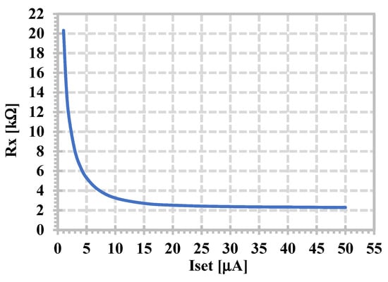
Figure 5.
Simulated parasitic resistance Rx with different Iset.
Figure 6 shows the simulated magnitude and phase frequency responses of the LPF, HPF, BPF, and BSF with C1 = C2 = 20 pF and Iset = 20 µA. Figure 7 shows the simulated magnitude and phase frequency responses of the APF. The filters offer a 3.23 MHz of the natural frequency. Thus, it is evident from Figure 6 and Figure 7 that the proposed current-mode filter can realize the five standard filtering functions in the same circuit without inverted input signal requirements.
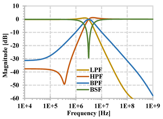
Figure 6.
Simulated magnitude and phase frequency responses of the LPF, HPF, BPF, and BSF.
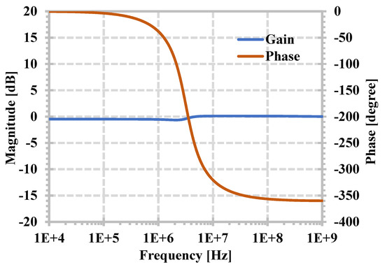
Figure 7.
Simulated magnitude and phase frequency responses of the APF.
The tuning capability of the proposed current-mode filter was tested by varying the bias current Iset. The simulated magnitude frequency response is shown in Figure 8. The natural frequency was (0.724, 1.51, 3.47) MHz when the bias current Iset was (2, 5, 40) µA, respectively.
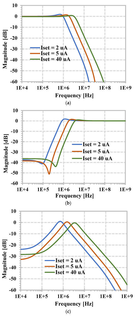
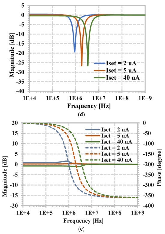
Figure 8.
Simulated magnitude frequency responses with Iset = 2, 5, 40 µA, (a) LPF, (b) HPF, (c) BPF, (d) BSF, and (e) APF.
The LPF was used to test the linearity of the proposed current-mode filter. The input signal has an in-band frequency of 10 kHz and the amplitude was varied. Figure 9 shows the simulated total harmonic distortion (THD) of the current-mode filter when the input amplitude was varied. The THD was 1.038% when the amplitude was 70 µA (140 µAp–p). Figure 10 shows the equivalent output current noise of the LPF. The integrated current noise over the bandwidth of 3.23 MHz was calculated to be 17.13 nA, giving a dynamic range of 69.2 dB.
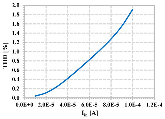
Figure 9.
Simulated THD of the LPF with different amplitudes of Iin.
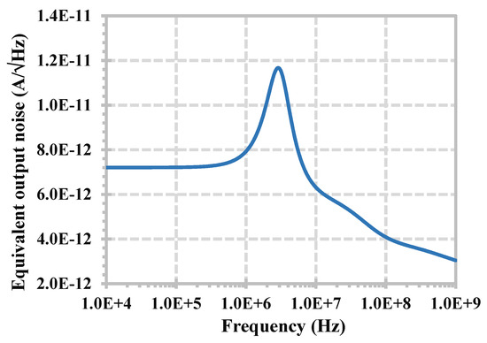
Figure 10.
The equivalent output current noise of the LPF.
Figure 11 shows the simulated frequency responses of the LPF, HPF, BPF, BSP, and APF when the temperature was set to −30, 27, and 85 °C. Figure 12 shows the simulated frequency responses of the filter when the voltage supply was set to 0.975 V, 1 V, and 1.25 V (1 V ± 5%). In both cases the curves overlapped or closed each other.
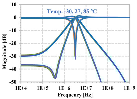
Figure 11.
The frequency response of the LPF, HPF, BPF, BSF, and APF with temperature corners.
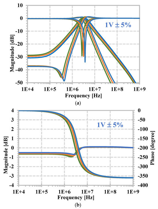
Figure 12.
The frequency response of, (a) LPF, HPF, BPF, BSF, and (b) APF, with voltage supply corners.
Figure 13 shows the simulated magnitude frequency responses of the proposed filter when the threshold voltage in CMOS process was varied by 10% (LOT tolerance), which represents a process variation. As can be seen, the curves are closed to each other.
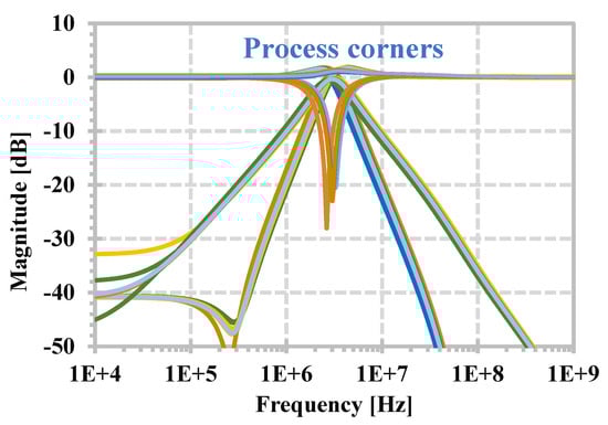
Figure 13.
Simulated magnitude responses of the proposed filter for process corners.
The proposed current-mode filter was compared with previous works, as shown in Table 4. The current-mode filters that use similar active devices, such as VD-EXCCCII [18], EX-CCCII in [31,32], and DV-EXCCCII in [33,34], were used for comparison. Compared with [31,32,33,34], the proposed current-mode filter can realize LPF, HPF, BPF, BSF, and APF without inverted and double input signal conditions. Compared with [18], the proposed current-mode filter uses an EX-CCCII of a lower complexity than the VD-EXCCII. However, the VD-EXCCII based filter in [18] can offer mixed-mode operation (i.e., VM, CM, TAM, TIM), but two resistors are required. Moreover, for the filter in [18], it is difficult to tune the natural frequency because the equation of natural frequency includes both parameters of the transconductance gm and resistance R. Thus, to tune the natural frequency without changing the quality factor, the condition gm = 1/R should be met.
Table 4.
Comparison of this work with selected analog filters.
4. Experimental Results
The EX-CCCII implementation used in this section to implement the current-mode universal filter is shown in Figure 14. The circuit is based on AD844 ICs and resistors. The resistors in the circuit are set as R1 = R2 = R3 = R4 to obtain Ix1 = Iz1+ = −Iz1− and R1c = R2c = R3c = R4c to obtain Ix2 = Iz2+ = −Iz2−. In this test, the resistors R1, R2, R3, R4, R1c, R2c, R3c, and R4c were 1 kΩ. The resistors Rx1 and Rx2 work as parasitic resistors of the EX-CCCII. The voltage-to-current (V/I) converter using AD844 and a resistor is used to convert the input voltage from a function generator to current inputs Iin (i.e., I1, I2, I3, and I4) (Iin = Vin/Rin), the example case for converting the voltage Vin to the input I1 (Iin) was shown in Figure 14. To measure the output currents, i.e., Io1, Io2, Io3, the current-to-voltage (I/V) converters are used (Vout = IoutRout), Figure 14 shows the example case for converting the current Io3 (Iout) to the output Vout. In this test, the resistors Rin and Rout were 10 kΩ. Thus, a unity voltage gain was obtained. Figure 15 shows a photo of the experimental setup. The circuits were supplied from ±5 V and 22-nF capacitances C1 and C2 were used. The measurement was performed using a Keysight DSOX1204G oscilloscope with a built-in signal generator.
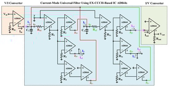
Figure 14.
Implementation of the EX-CCCII using AD844s to realize the current-mode universal filter.
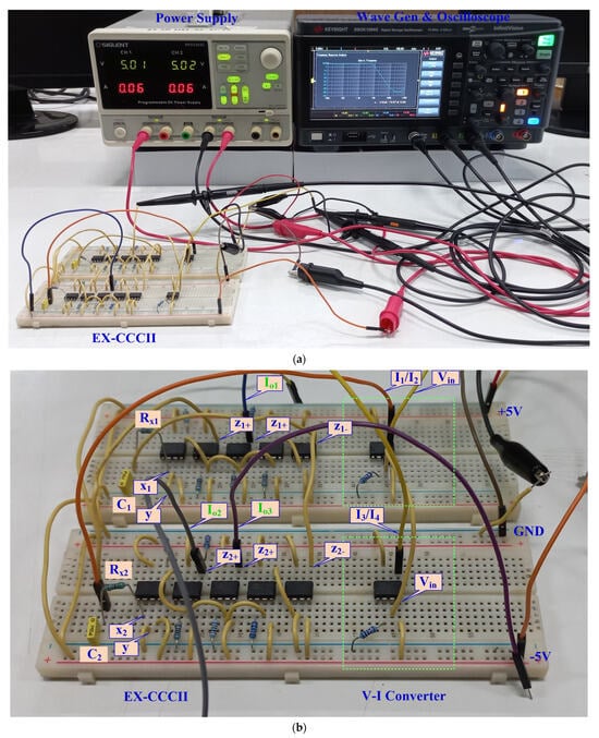
Figure 15.
(a) Experimental setup, (b) close-up of the EX-CCCII and V/I converter.
Figure 16a,b show the measured magnitude responses of the LPF, HPF, BPF, BSP, and APF with setting resistances Rx1 = Rx2 = 5 kΩ. The measured natural frequency was 1.343 kHz while the filter was designed for a natural frequency of 1.446 kHz, giving an error of 7.12%. This result confirms the workability of the proposed current-mode filter.
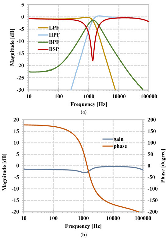
Figure 16.
Magnitude responses with setting resistances Rx1 = Rx2 = 5 kΩ for (a) LPF, HPF, BPF, BSF, and (b) APF.
Figure 17 shows the measured magnitude responses of the BPF when the resistances Rx1 and Rx2 (Rx1 = Rx2) are set to 15 kΩ (a), 10 kΩ (b), 5 kΩ (c), and 1 kΩ (d). From (6) and (7), the natural frequency can be determined using Rx1 = Rx2 while the quality factor (Q) can be selected using C1/C2. The capacitor values were fixed as C1 = C2 = 22 nF and the resistors Rx1 = Rx2 are given, resulting in Q = 1. By setting the resistor’s values from 15 kΩ, 10 kΩ, 5 kΩ, and 1 kΩ, the measured natural frequencies were found to be 0.469 kHz, 0.704 kHz, 1.343 kHz, and 6.668 kHz, respectively. The filter is designed for natural frequencies of 0.482 kHz, 0.723 kHz, 1.446 kHz, and 7.234 kHz, respectively. Thus, the errors were 2.69%, 2.62%, 7.12%, and 7.82%, respectively. This experimentation serves to confirm the tuning capability of the current-mode filter expressed in (6).
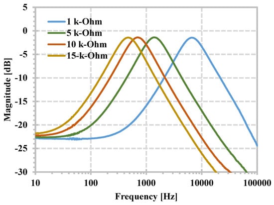
Figure 17.
Measured magnitude frequency responses of the BPF with setting resistances Rx1 = Rx2 for (1, 5, 10, 15) kΩ.
5. Conclusions
In this study, a new electronically tunable current-mode universal analog filter with multiple inputs and multiple outputs is proposed. The filter employs only one EX-CCCII and two grounded capacitors. The topology can realize five standard filtering functions of low-pass, high-pass, band-pass, band-stop, and all-pass responses without changing the internal configuration of the filter by selecting the appropriate input and output signals. The inverted input signal and input matching conditions are absent for obtaining these filtering functions. The natural frequency of all filter responses can be electronically controlled. The proposed filter was simulated by SPICE and confirmed through experimental testing using IC AD844s.
Author Contributions
Conceptualization, M.K., F.K. and T.K.; methodology, M.K., F.K. and T.K.; software, M.K. and F.K.; validation, M.K., F.K. and S.T.; formal analysis, M.K. and T.K.; investigation, M.K., F.K. and T.K.; resources, M.K.; data curation, M.K. and F.K.; writing—original draft preparation, M.K., F.K., T.K. and S.T.; writing—review and editing, M.K., F.K., T.K. and S.T.; visualization, M.K. and F.K.; supervision, M.K. and F.K.; project administration, M.K. and F.K.; funding acquisition, M.K. All authors have read and agreed to the published version of the manuscript.
Funding
This work was supported in part by the University of Defence within the Organization Development Project VAROPS.
Data Availability Statement
Data are contained within the article.
Conflicts of Interest
The authors declare no conflicts of interest.
References
- Roberts, G.; Sedra, A. All current-mode frequency selective circuits. Electron. Lett. 1989, 25, 759–761. [Google Scholar] [CrossRef]
- Toumazou, C.; Lidgey, F.J.; Haig, D.G. Analogue IC Design: The Current-Mode Approach; Peter Peregrinus: London, UK, 1990. [Google Scholar]
- Sedra, A.; Smith, K. A second-generation current conveyor and its applications. IEEE Trans. Circuit Theory 1970, 17, 132–134. [Google Scholar] [CrossRef]
- Fabre, A.; Saaid, O.; Wiest, F.; Boucheron, C. Current controlled bandpass filter based on translinear conveyors. Electron. Lett. 1995, 31, 1727–1728. [Google Scholar] [CrossRef]
- Maheshwari, S. Current conveyor all-pass sections: Brief review and novel solution. Sci. World J. 2013, 2013, 429391. [Google Scholar] [CrossRef] [PubMed]
- Maheshwari, S. Voltage-mode full-wave precision rectifier and an extended application as ASK/BPSK Circuit Using a Single EXCCII. Int. J. Electron. Commun. 2018, 84, 234–241. [Google Scholar] [CrossRef]
- Maheshwari, S. Realization of simple electronic functions using EXCCII. J. Circuits Syst. Comput. 2017, 26, 1750171. [Google Scholar] [CrossRef]
- Agrawal, D.; Maheshwari, S. Current-mode precision full-wave rectifier circuits. Circuits Syst. Signal Process. 2017, 36, 4293–4308. [Google Scholar] [CrossRef]
- Das, R.; Paul, S.K. Resistorless current mode precision rectifier using EXCCII. Analog. Integr. Circuits Signal Process. 2020, 103, 511–522. [Google Scholar] [CrossRef]
- Kapoulea, S.; Psychalinos, C.; Elwakil, A.S. Single active element implementation of fractional-order differentiators and integrators. Int. J. Electron. Commun. 2018, 97, 6–15. [Google Scholar] [CrossRef]
- George, M.A.; Bhavani, I.V.L.D.; Kamath, D.V. EX-CCII Based FOPID controller for electric vehicle speed control. In Proceedings of the 2020 IEEE International Conference on Distributed Computing, VLSI, Electrical Circuits and Robotics (DISCOVER), Udupi, India, 30–31 October 2020; pp. 47–51. [Google Scholar]
- Joshana, R.; Singh, Y.S.; Ranjan, A. An electronically tunable fractional order inductor employing VD-EXCCII. Int. J. Electron. Commun. 2023, 174, 155055. [Google Scholar] [CrossRef]
- Agrawal, D.; Maheshwari, S. Design and implementation of current mode circuit for digital modulation. Integration 2021, 78, 118–123. [Google Scholar] [CrossRef]
- Kumar, A. Single EXCCII-based analog multiplier structure. J. Circuits Syst. Comput. 2021, 30, 2150107. [Google Scholar] [CrossRef]
- Chaturvedi, B.; Kumar, A. Single EXCCII based square/triangular wave generator for capacitive sensor interfacing and brief review. VLSI Post-CMOS Electron. Devices Circuits Interconnects 2019, 2, 329–349. [Google Scholar] [CrossRef]
- Maheshwari, S.; Agrawal, D. High performance voltage-mode tunable all-pass section. J. Circuits Syst. Comput. 2015, 24, 1550082. [Google Scholar] [CrossRef]
- Maheshwari, S. Tuning approach for first-order filters and new current-mode circuit example. IET Circuits Devices Syst. 2018, 12, 478–485. [Google Scholar] [CrossRef]
- Faseehuddin, M.; Herencsar, N.; Albrni, M.A.; Sampe, J. Electronically tunable mixed-mode universal filter employing a single active block and a minimum number of passive components. Appl. Sci. 2021, 11, 55. [Google Scholar] [CrossRef]
- Agrawal, D.; Maheshwari, S. Electronically tunable mixed-mode third-order universal filter using a single EX-CCCII. Aust. J. Electr. Electron. Eng. 2022, 19, 307–323. [Google Scholar] [CrossRef]
- Banerjee, K.; Joshi, M.; Sarkar, C.; Biring, S. Low-frequency resistorless electronically tunable quadrature oscillator based on an EX-CCCII. J. Electron. Mater. 2023, 52, 1–6. [Google Scholar] [CrossRef]
- Kumari, A.; Ranjan, A. Extra-X current controlled current conveyor based resistorless current mode quadrature sinusoidal oscillator. Int. J. Appl. Eng. Res. 2018, 13, 1–5. [Google Scholar]
- Bhatt, V.; Ranjan, A.; Singh, Y.S. Resistorless Chua’s diode implementation for chaotic oscillation employing single EXCCCII. Int. J. Electron. Commun. 2022, 156, 154398. [Google Scholar] [CrossRef]
- Li, Y.; Hou, J. Pathological models of EXCCCII and its applications in oscillator synthesis. Wuhan Univ. J. Nat. Sci. 2022, 26, 115–122. [Google Scholar] [CrossRef]
- Singh, P.; Nagaria, R.K. Single EX-CCCII based electronically tunable current mode instrumentation amplifier. Eng. Rev. 2022, 42, 1–16. [Google Scholar] [CrossRef]
- Agrawal, D.; Maheshwari, S. Cascadable current mode instrumentation amplifier. Int. J. Electron. Commun. 2018, 94, 91–101. [Google Scholar] [CrossRef]
- Agrawal, D. Electronically Tunable Grounded Immittance Simulators Using an EX-CCCII. Int. J. Electron. 2020, 107, 1625–1648. [Google Scholar] [CrossRef]
- Singh, P.; Nagaria, R. Low voltage EX-CCCII based on quasi-floating gate technique and its application as precision rectifier. Int. J. Electron. Commun. 2022, 155, 154378. [Google Scholar] [CrossRef]
- Singh, P.; Varshney, V.; Kumar, A.; Nagaria, R.K. DV-EXCCCII–based electronically tunable voltage mode all-pass filter. Lect. Notes Electr. Eng. 2021, 777, 485–494. [Google Scholar] [CrossRef] [PubMed]
- Maheshwari, S.; Agrawal, D. Cascadable and tunable analog building blocks using EX-CCCII. J. Circuits Syst. Comput. 2017, 26, 1750093. [Google Scholar] [CrossRef]
- Singh, P.; Varshney, V.; Kumar, A.; Nagaria, R.K. DV-EXCCCII–based electronically tunable current mode filter. Lect. Notes Electr. Eng. 2021, 777, 235–245. [Google Scholar] [CrossRef] [PubMed]
- Agrawal, D.; Maheshwari, S. Current mode filters with reduced complexity using a single EX-CCCII. Int. J. Electron. Commun. 2017, 80, 86–93. [Google Scholar] [CrossRef]
- Agrawal, D.; Maheshwari, S. High-performance electronically tunable analog filter using a single EX-CCCII. Circuits Syst. Signal Process. 2021, 40, 1127–1151. [Google Scholar] [CrossRef]
- Singh, P.; Nagaria, R.K. DV-EXCCCII based resistor-less current-mode universal biquadratic filter. Adv. Technol. Innov. 2023, 8, 12–28. [Google Scholar] [CrossRef]
- Singh, P.; Nagaria, R.K. Electronically tunable DV-EXCCCII-based universal filter. Int. J. Electron. Lett. 2020, 9, 301–317. [Google Scholar] [CrossRef]
Disclaimer/Publisher’s Note: The statements, opinions and data contained in all publications are solely those of the individual author(s) and contributor(s) and not of MDPI and/or the editor(s). MDPI and/or the editor(s) disclaim responsibility for any injury to people or property resulting from any ideas, methods, instructions or products referred to in the content. |
© 2024 by the authors. Licensee MDPI, Basel, Switzerland. This article is an open access article distributed under the terms and conditions of the Creative Commons Attribution (CC BY) license (https://creativecommons.org/licenses/by/4.0/).