1. Introduction
Power management has become crucial in modern Systems on Chips (SOCs) with many voltage rails for several parts of the chip. Previously, power management was usually an off-chip integrated circuit (IC) on the printed circuit board (PCB) that generates the required rails. However, now, the power management unit (PMU) is integrated on the same die with one or more PMUs distributed across the chip. However, proper power delivery for several rails is proving very challenging to meet the requirements of IR drops and electromigration (EM) concerns.
Having one or more central PMUs to supply the whole chip is proving very difficult, and more localized mini regulators are now needed to provide proper rails. Linear dropout (LDO) regulators are proving popular [
1,
2]. Unfortunately, LDOs can only supply rails lower than the input supply. If a higher rail is needed, as is the case in embedded memories, switching regulators are used. Using inductor-based regulators requires the use of an external inductor which requires a pad. So, having multiple instances will be problematic and require bulky inductors that use precious PCB area. Single-inductor multiple-output (SIMO) regulators [
3,
4,
5] are gaining popularity, but still require two pads and this is very complex. The other option is to use switched-capacitor (SC) regulators.
SC regulators can use external capacitors for their flying and output capacitors [
6] or integrated capacitors [
7,
8,
9]. SC regulators usually use very large capacitors in the range of nFs, making their area very large. Some implementations distribute the area allocated for the capacitors between output and flying capacitors [
7], while others use a zero output capacitor and dedicate all the area to the flying capacitor [
10]. Usually, they use a combination of MOM + MOS capacitors [
11] and sometimes add MIM capacitors [
9]. The use of MIM capacitors usually means an extra cost due to the use of extra masks in the fabrication process. Additionally, not all fabs and technology nodes offer MIM capacitors.
Another popular technique is the multiphase operation [
10,
12], where several converter units operate out of phase or with different phases. This helps reduce the ripples on the output of the SC regulator by effectively reducing the discharge time of the output.
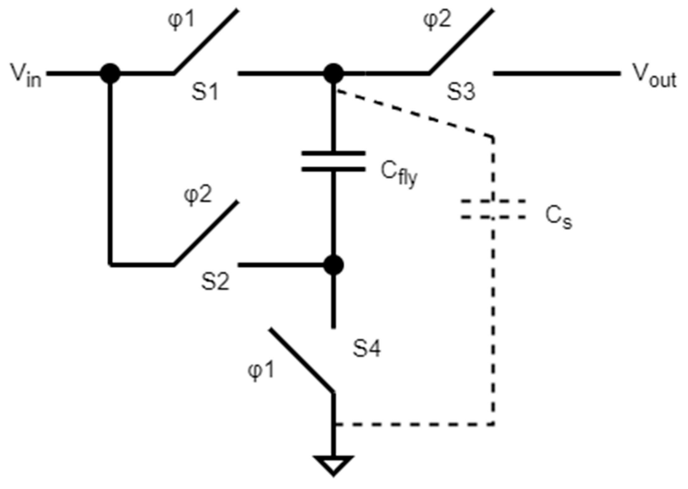
The charge pump, also known as a doubler, is among the most widely used SC circuits. The charge pump has four switches and a flying capacitor C
fly as shown in
Figure 1. The operation starts by closing S1 and S4 with one clock phase (φ1), allowing C
fly to charge to V
in. Then, S4 and S1 are opened followed by the closing of S2 and S3 using φ2. Now the capacitor C
fly is connected between V
in and V
out. Since the capacitor C
fly had an initial voltage across its terminals equal to V
in, V
out will have a voltage of 2 × V
in. The output will be lower due to losses from the stray capacitance from the top plate to the ground [
13]. V
out at zero load can be calculated as:
where L represents the losses due to the stray capacitance, which can be expressed as follows:
where α = C
s/C
fly and C
s is the stray capacitance from the top plate to the ground.
Normally, charge pumps are connected in parallel to increase the driving capability of the circuit. They are organized as tiles used as building blocks for bigger systems.
Section 2 will discuss the proposed system, circuit implementations, and the added features to the circuits, such as the soft start and the current bleeder.
Section 3 will present the simulation results, followed by
Section 4, where the results are discussed. The work is compared to the current state-of-the-art implementations and is then followed by the conclusion of the work in
Section 5.
2. Circuit Description
The proposed regulated charge pump consists of eight adaptable tiles, an always-on (AON) tile, a resistor divider to sense the output voltage using a scaled version of the output voltage VCC, a pseudo-6-bit analog-to-digital converter (ADC) whose output code controls the eight charge pump tiles, a small output capacitor, and a current bleeder as shown in
Figure 2. The circuit also has some logic used to create the soft start. A modular design approach is chosen to allow for scaling the output current by increasing the number of tiles controlled by the ADC.
2.1. Charge Pump
Each tile consists of 32 charge pump units connected in parallel. The Dickson charge pump [
14] is used in the system. Each of the 32 charge pumps operates with two complementary phases of 32 phases of a 200 MHz clock. The charge pump circuit is based on the work of [
15]. The schematic of the differential charge pump implementation is shown in
Figure 3. Cm1, Cm2, Cl1, Cl2, Cl3, and Cl4 are all implemented using PMOS devices but drawn as capacitors for simplicity. When enabled (PU is high and PUz is low), the charge pump main capacitors, Cm1 and Cm2, are charged through MN1 and MN2. The toggling of Phi1/Phi2 charges VCC1 and VCC2 to switch between VDD and 2 × VDD. Cl1 and Cl2 act as level translators and ensures that the gates of MN3, MN4, MN5, and MN6 are biased properly by switching between VDD and 2 × VDD. The logic created by the NAND gate and the two inverters ensures that MN3, MN4, MN5, and MN6 are closed before MP1, MP2, MP3, and MP4 are opened. Cl3 and Cl4 also act as level translators, properly biasing the PMOS output devices. VCC is connected to VCC1 or VCC2 when they are charged to 2 × VDD. This way, VCC stays at a 2 × VDD level during the circuit operation. MN6 and MN7 are used to discharge Cm1 and Cm2 (also Cl1, Cl2, Cl3, and Cl4) when the charge pump is turned off.
The area of this unit differential charge pump is small, 14.16 µm × 53.1 µm. The cell uses 2.5 V devices with a 3.3 V overdrive to support voltages up to 3.63 V. This device is chosen to avoid any electrical over-stress (EOS) and other reliability concerns in a boost converter.
2.2. Pseudo-ADC
The pseudo-6-bit ADC compares a scaled version of the output voltage (in this case, half the output voltage) to a reference voltage—generated internally using a reference current—and based on the difference, the ADC code changes. As the output voltage starts to droop due to leakage or high load, the error expected from the nominal value increases. As the error increases, the ADC output codes start to increase. The increase in ADC output indicates an increased error and prompts the system to use more charge pumps to reduce the error. As the error decrease, so does the number of charge pumps engaged. This method, in addition to the usage of multiphase operation, results in reduced ripples. However, the real advantage is the increased response to fast transients. As soon as the system detects a drop in the output, extra charge pumps are added online to reduce the droop, and at the same time, they are removed when the output increases to reduce the overshoot. This results in a system capable of supporting transients as fast as a 100 ps change from zero load to 6 mA, and the output voltage stays within 4% of the expected value.
The pseudo-ADC is shown in
Figure 4. The ADC has a resistor ladder that generates six levels to compare to: vref, vref—1 × least significant bit (LSB), vref—2 × LSB, vref—4 × LSB, vref—8 × LSB, and vref—16 × LSB. The iref current comes from the Bandgap (BG) circuit. The resistors should use the same unit resistor used by the BG to track its variation to get an accurate reference. There is a programable resistor that helps change the value of vref as needed through a digital code.
The value of vref is half the converter output voltage. This value is chosen to be high enough for the comparator shown in
Figure 5 to operate properly. The circuit has 32 dynamic comparators, each using one of the 32 phases. The phases and the reference value for each comparator are shown in
Figure 4. Low loads need small numbers of charge pumps. The comparators are arranged so that at very small loads, only the AON charge pumps are used, and the rest of the charge pumps are disabled.
As the current increases, the system starts adding more charge pumps. Phases of the newly added charge pumps are taken care of. When a charge pump is added, it is made out of phase with the previously enabled charge pump. When two charge pumps are added, they are driven out of phase. When four charge pumps are added, the four charge pumps are driven with a 90° phase difference. The same applies to 8 phases and 16 phases. Having the phases distributed this way ensures the output is left undriven for the least amount of time, hence the low ripples. Additionally, this distribution helps speed up the system’s response to high-speed transients. The exact phases’ distribution is shown in
Table 1. The schematic of the comparator is shown in
Figure 5 [
16].
When the CLK is high, MN1 is turned on while MP1 and MP2 are turned off. If Vinp is higher than Vinn, this will cause a higher current to pass through M2 than M3. This will make midn voltage go lower than midp. MN4/MP3 and MN5/MP4 act as cross-coupled inverters. When midn decreases, MN4 sees a higher VGS driving outn to zero, which drives outp to supply. Since the cross-coupled back-to-back inverters act as a positive feedback loop, a reset for the comparator is needed every clock cycle, which happens when the CLK is low enabling MP1 and MP2, which pulls outp and outn to the supply. An SR latch ensures that the comparator maintains its output value without being reset.
2.3. Soft Start and Current Bleeder
Because of the relatively small output capacitor, there is a potential overshoot issue. If there is a zero load and the output overshoots, it will settle on a higher-than-expected value. Output may settle on this high value and will remain there for a long period. This can happen at startup and during transitioning from maximum load to zero loads.
At startup, all tiles are engaged because the output is still low. This will result in a large overshoot. To solve this issue, the circuit starts in a mode called soft start, where all tiles are disabled, and only a small portion of the AON charge pumps are active. Only after a certain period an OK signal is asserted high. The OK signal enables all the tiles, which will not be engaged at this point because the output is not loaded yet. It is a common practice to have an OK signal that tells the SOC that the regulator is ON and ready to enable the load. Enabling the load before the OK signal might result in (1) a longer startup time, (2) may suffer from a significant droop at the output that will take longer-than-expected time to recover from, and (3) a potential wrong operation of the load if the output voltage is less than the acceptable operational range.
Figure 6 shows the schematic of the proposed OK circuit. The circuit consists of 9 D flip-flops. The first flip-flop has the Qbar connected to the D while the clock is triggered normally. The rest of the flip-flops have their clock connected to the Q output of the previous stage. This configuration is a clock divider where every flip-flop’s output has half the clock’s frequency driving it. All stages have their reset disabled except the 1st stage. At startup, the output of the last flip-flop is high. Once it is triggered low, the inverter feeds back to the first flip-fop and resets it, essentially stopping all the toggling in all the stages. This means the output will go up and stay up indefinitely or until the supply decreases to zero. The input clock is a 200 MHz which means a duration of 5 ns. To calculate the delay, the following equation is used:
where D
OK is the OK delay, T
CLK is the clock duration, and n is the number of stages. Since nine stages are used, the delay will be 5 ns × 2
(9−1) = 1.28 us. The OR gate at the end bypasses the OK circuit if needed. When the BYPASS signal is low, the OK will go high after the specified delay. When BYPASS is high, the OK is high regardless of the delay implemented and the clock used at the circuit’s input.
A similar situation occurs during transitioning from maximum load to zero when a lot of charge pumps are active. If the change from high to low is rapid, an overshoot will be observed, and the output will settle on a wrong value. A solution to this is to add a simple current bleeder circuit, shown in
Figure 7. The idea is to maintain a small amount of current that forces the output to discharge to the expected level. The current bleeder has 2 bits of programmability to control the amount of current. The current bleeder current ranges from 50 uA when config<1:0> = 11 to 12.5 uA when config<1:0> = 00 at 3 V output. The values are too small to affect the startup or cause a short between the output and the ground. For lower voltage outputs, the range changes, so the programmability is here to ensure adequate bleeded current for several ranges of outputs.
3. Results
Figure 8 shows the output ripple voltage under several loads, voltage ripples across different loads, and line regulation across different loads. Voltage ripples are less than 35 mV at maximum load.
Figure 9 shows the startup of the regulator when enabling and disabling the OK circuit. The circuit starts in less than 50 ns while the OK circuit is disabled but settles ~50 mV higher than the regulated value and increases to 80 mV across PVT. The current bleeder circuits make sure it discharges to the final value. If the current bleeder is disabled, the output will settle on the final value. With the OK circuit enabled, the circuit starts in approximately 650 ps. The OK will go high in 1.28 us, as explained earlier. The slow startup with the OK is due to having fewer charge pumps enabled during a soft start. Only 16 charge pumps are enabled during a soft start. If the soft start is disabled, 288 charge pumps are enabled at startup.
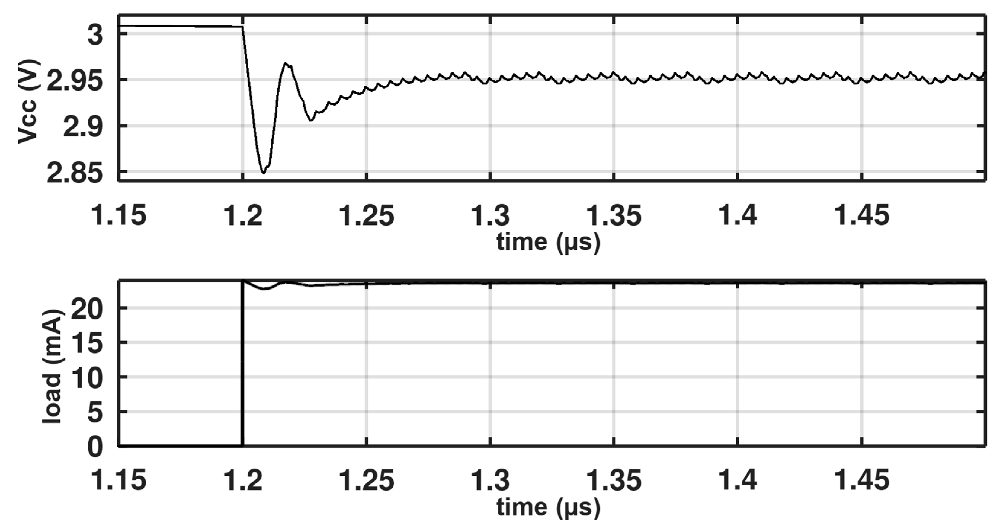
Figure 10 shows the transient response to a load step changing from 0 to 6 mA in 100 ps. The load is implemented as a 500 Ω resistor with a transistor in series acting as a switch. The transistor gate is turned from zero to 1.8 V at 100 ps. This transition is very aggressive, but the system can recover quickly and continue operating as expected.
Figure 11 shows the response going from 6 mA to zero loads.
The undershoot due to the fast transition of load from low to high is approximately 3% of the output and takes approximately 500 ns to stabilize and continue working normally. The overshoot due to the fast transition from maximum to zero load is approximately 1%, and the current bleeder ensures that the output discharges back to its nominal value. Efficiency versus several loads is shown in
Figure 12. Efficiency is calculated as P
out/P
in. P
out is our output voltage (3 V) multiplied by the load current, whereas P
in is the input voltage (1.8 V) multiplied by all the currents consumed from this supply. A peak efficiency of 44% is achieved at maximum load (6 mA). The maximum theoretical efficiency is 83.3%. The system efficiency is relatively low because of using 32 comparators for the charge pumps instead of using one comparator for all the charge pumps. Additionally, the converter uses 2.5 V devices with a 3.3 V overdrive which is large and introduces more switching losses. Another factor that degrades the efficiency is the losses in the charge pumps due to the usage of MOS capacitors to reduce the silicon area which have higher parasitic losses.
4. Results Discussion
The newly proposed method of having different reference voltages between the charge pumps, compared to the conventional method of having just one reference for all charge pumps, achieves better response and lower ripples at full load. The proposed method compared to the conventional approach is shown in
Figure 13. The proposed method has much lower ripples (3× reduction) and a fast transient response.
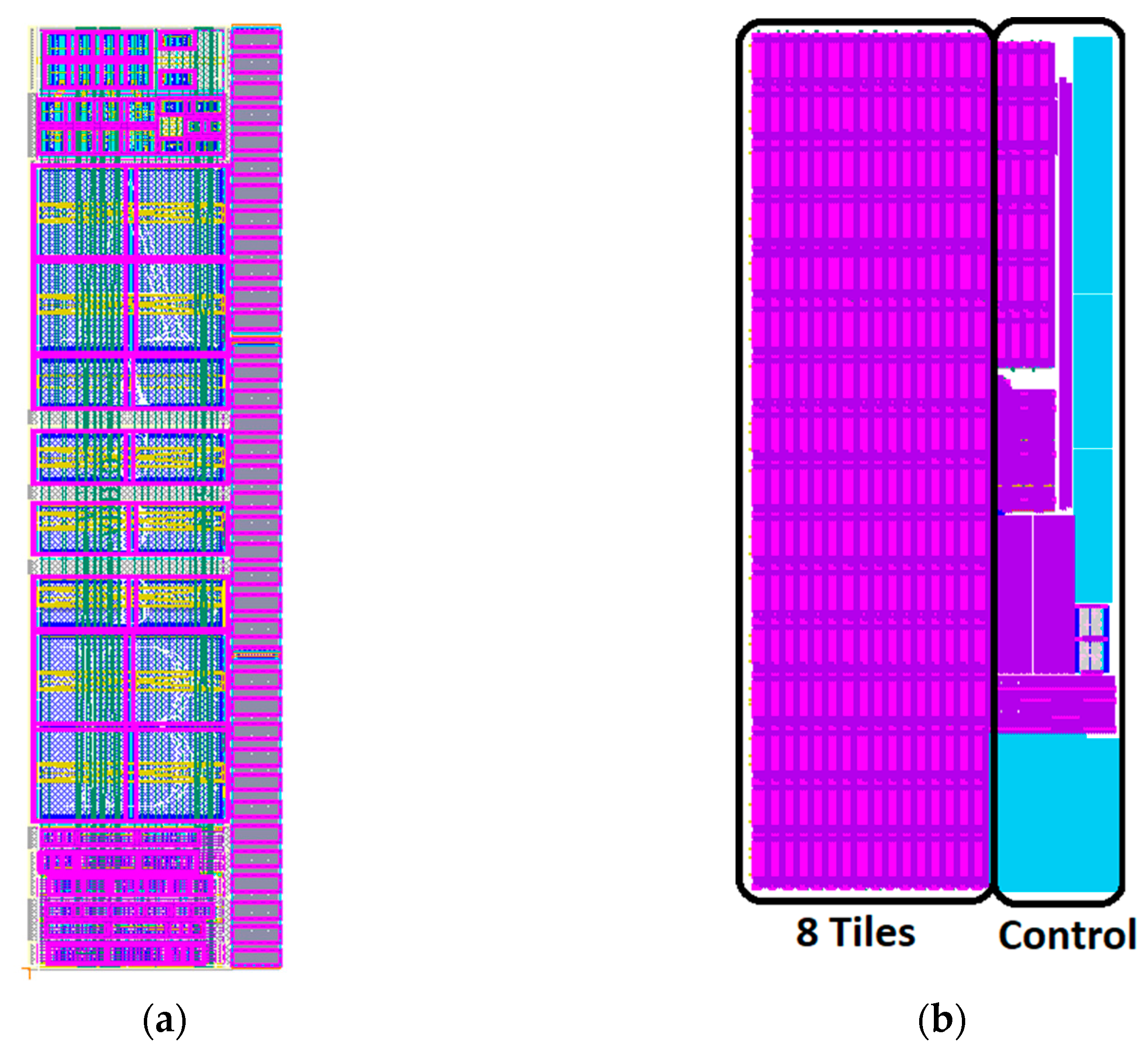
The layout of the unit charge pump is shown in
Figure 14a. The area of the unit charge pump is compact, using 14.16 µm × 53.1 µm. They can be stacked together to create large tiles as being used in the proposed design, which uses 32 units per tile.
Figure 14b shows the floorplan for the proposed system, taking an area of 337.395 µm × 881 µm.
Figure 15b shows the tiles stacked together and the control block with the AON tiles, 32 comparators, the current bleeder, the output capacitor, the resistor divider, and logic needed to control and drive the tiles.
Extra tiles can be added to increase the current on the expense of area. The added tiles share the same control and can be placed beside the control block. Adding 24 extra tiles will increase the load current to 24 mA, and the area will be 0.9726 mm
2, provided the tiles are placed as 2 ∗ 8 tiles on each side of the control block. While adding the extra tiles, a significant modification is made while connecting them; they are connected with a 90-degree phase difference. In this case, lower ripples are achieved while adding the extra tiles.
Figure 15 shows the behavior of the 32 tiles when connected as mentioned above while changing the load from 0 to 24 mA in 100 ps. The ripples are 3× lower than the normal eight tiles configuration.
Table 2 compares the proposed converter with the state-of-the-art literature.
For the switched-capacitor regulators, Figure of Merits (FOMs) were developed to compare the performance of several converters as proposed in [
12]. Still, there is no FOM to compare the transient behavior of switched-capacitor regulators. There is a FOM to compare the transient response in linear dropout (LDO) regulators proposed in [
17]. FOM
LDO is defined as follows:
where T
R is the response time and can be calculated as follows:
where C is the decoupling capacitor the LDO uses, I
Q is the quiescent current of the LDO, ΔV
OUT is the change in output due to the load change, and I
MAX is the specified max current for the LDO.
A FOM is proposed to compare the transient response of the SC regulators as follows:
where T
R is the response time, C is C
FLY + C
OUT, ΔV
OUT is the change in output due to the load change, ƞ
peak the peak efficiency, and I
MAX is the specified max current for the regulator. The scaling factor, 1E15, is to make the number easily readable. As the number decreases , the regulator has a better transient response.


