Abstract
Deep neural networks (DNNs) and Convolutional neural networks (CNNs) have improved accuracy in many Artificial Intelligence (AI) applications. Some of these applications are recognition and detection tasks, such as speech recognition, facial recognition and object detection. On the other hand, CNN computation requires complex arithmetic and a lot of memory access time; thus, designing new hardware that would increase the efficiency and throughput without increasing the hardware cost is much more critical. This area in hardware design is very active and will continue to be in the near future. In this paper, we propose a novel 8T XNOR-SRAM design for Binary/Ternary DNNs (TBNs) directly supporting the XNOR-Network and the TBN DNNs. The proposed SRAM Computing-in-Memory (CIM) can operate in two modes, the first of which is the conventional 6T SRAM, and the second is the XNOR mode. By adding two extra transistors to the conventional 6T structure, our proposed CIM showed an improvement up to 98% for power consumption and 90% for delay compared to the existing state-of-the-art XNOR-CIM.
1. Introduction
DNNs are currently the infrastructure for many AI applications including recognition and detection tasks [1,2,3]. Furthermore, CNNs are the most popular form of DNNs, because of their ability to achieve very high accuracy by applying a very deep hierarchy of layers. Moreover, a Fully Connected layer (FC) is the most popular layer in CNNs. In an FC layer, every neuron in the output feature map is a weighted sum of every input neuron in the input feature map, as shown in Figure 1, where the FC layers form from Fully Connected and non-linear layers. Thus, this results in a requirement for a massive amount of storage, and complex computation [4], both in cloud and edge. However, the superior accuracy of DNNs came with the cost of high computational complexity and memory access time. Thus, many DNN models, each having a different architecture, have been developed over the last decade to address this issue [5,6].
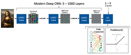
Figure 1.
Convolutional Neural Networks.
In the last decade, there has been an enormous enhancement in DNN algorithms that have exceeded human accuracy. One of these recent algorithms proposed binarizing the activations to [+1, −1], such that the Multiply-And-Accumulate (MAC) operation becomes an XNOR operation [7]. Another algorithm proposed to ternarize the activations with the weights was still binarized such that the MAC operation became an XOR, AND, Bitcount [8].The initial binarized XNOR-Net achieved and . However, the Ternary Inputs and Binary Weights (TBN-Net) outperformed the XNOR-Net by up to 5.5% on the ImageNet classification task and up to 4.4% on the PASCAL VOC object detection task. TBNs also reduce computational complexity. However, this reduction comes with the high cost of row-by-row memory access, which eventually controls the speed and energy efficiency of DNN hardware. Thus, designing hardware to support the efficient processing of DNNs and, especially, to support DNNs with ternary activations and binary weights that can increase energy efficiency and throughput without increasing the hardware cost is very critical, and a scorching research topic in the machine learning community.
The current mainstream hardware unit in the cloud is the graphical processing unit (GPU). This is due to its simplicity in programming in addition to its achieving very high accuracy. They are commonly used to train DNNs where a group of GPUs is connected, which would consume hundreds to thousands of Watts of power. Now, application-specific-integrated circuits (ASICs) or domain-specific architectures, such as Tensor-processing-unit (TPUs), to improve energy efficiency, are becoming more popular, and could, eventually, be the primary source to support both cloud and edge applications. The main operation in DNN hardware is the vector–matrix multiplication (VMM) operation between the activations (inputs) and the weights, which, eventually, becomes a MAC operation. This operation is directly correlated to the main challenge in DNN hardware design, which is the repeated movement back and forth from the memory units to the computing units. That being said, GPUs and TPUs are still not solving this problem, with the main cores or processing elements (PEs) in their design architecture still far from off-chip memory (DRAM), or even on-chip memory. Considering this, In-Memory-Computing (IMC), or Computing-in-Memory (CIM), has been proposed as a potential solid candidate to speed up the VMM operations.
2. Trends and Challenges of SRAM-CIM for AI Applications
2.1. Principle of CIM
Computing-in-Memory (CIM) is considered the best candidate to speed up the VMM operations, due to the crossbar nature of the memory sub-array, which, eventually, plays a significant role in decreasing the power consumption on the chip by decreasing the off-chip memory access (DRAM access). The popularity of CIM comes from combining two concepts of memory access and computation in one bit cell, instead of reading out every row of the bit cells, which decreases the power consumption correlated with the on-chip memory accesses. DNN layer weights are mapped into the memory bit cell as the conductance of the memory bit cells by taking advantage of the voltage already stored in the bit cell. In addition, the inputs (activations) are introduced as perpendicular rows as new voltages to the memory sub-array. Hence, this results in an introduction to the analog side inside the memory sub-array. Due to this analog computation result, the Sense Amplifier (SA) in the traditional memory designs is replaced with the analog–digital converter (ADC) to outcome a quantized multi-bit output.
2.2. Challenges of SRAM-CIM
CIM macros could be constructed with Static random-access memory (SRAM) or Embedded non-volatile memory (eNVM) (e.g., RRAM). However, from the available technological outlook, and with aggressive node scaling, it is now possible now to store almost all of the weights on-chip (e.g., 256 Mb SRAM achieved at 7 nm by TSMC [9]). As a result, SRAM-CIM is considered the strongest candidate to be implemented in AI accelerators. Nonetheless, SRAM-CIM has several design challenges. The biggest challenge that SRAM-CIM macros face is the design of ADC. Thus, choosing the best ADC architecture, that does not increase on-chip power consumption and occupy a significant portion of the die area, is very challenging. The number of rows selected simultaneously determines the analog partial sum magnitude for the output columns, which determines the resolution of the ADC. It is considered critical to design an ADC with a fixed number of bits, as every design of SRAM-CIM is considered a particular case. Moreover, ADC design for CIM does not require high resolution, as 3–6 bits would be enough for most data sets. ADC for CIM requires a large area, as each output column should be followed with one ADC to increase the VMM parallelism. Moreover, the ADC offset causes process variations, which, in return, slightly decreases the accuracy of the DNN if SRAM-CIM architecture is used [10]. Another challenge SRAM-CIM faces, that arises from aggressive shrinking of the transistor feature size in recent years, as we are currently heading into 2 nm node technology, is the single event transient (SEU) and the double-node upset (DNU). The strike of the particles, such as protons, neutrons electrons, and heavy ions, may result in change in the state of a single node or two nodes, as stated in [11], where the storage elements such SRAM memory cells and flip-flop suffer from this issue. Off-chip DRAM access is another challenge for SRAM-CIM. Although it was earlier assumed that most weights would be stored on-chip in an ideal case, this is not always so, as on-chip memory capacity is not always large enough to hold all the weights. In some cases, the DNN model size exceeds the GB level for some AI tasks, such as natural language processing. Thus, increasing the on-chip capacity means increasing the area, which might be unrealistic from a manufacturing cost perspective. Thus, if we cannot increase the die area, and most of the weights are stored off-chip (DRAM), a recent work looked into this case and reported a 40–80% decrease in performance [12]. Another potential challenge that faces SRAM-CIM, or even CIM designs in general, is reverse engineering, which comes from the fact that most of the weights can be stored on-chip, which raises a software/hardware security issue, since most DNN models need a massive amount of datasets to train, and, thus, require days to weeks, which could inspire adversaries to manipulate the chip weights.
2.3. SRAM-CIM Designs
Ref. [13] is one of the earliest SRAM-CIM designs, where the authors proposed a 6T design that used a split-wordline. Another recent work is XNOR-SRAM [14], in which the authors proposed a 12T SRAM cell that computes the ternary XNOR-and-accumulate (XAC) operations without the need for row-by-row data access. This is achieved by simultaneously turning on all 256 rows, which eventually forms a resistive voltage divider in one column. The bit cell produces the dot-product XNOR operations that are read by the bitline (RBL), and this analog voltage (RBL) is, then, digitized with a column-multiplexer 11-level flash analog-to-digital converter (ADC). The ADC plays a significant role in this design, as the authors investigated the (XAC) values and found that the results were highly concentrated around zero. With such results, they limited the quantization range to the region that covered the most data, and, then, each quantization referenced in the XAC would map to a unique (Vref) for the flash ADC. The design reported Another design is the CONV-SRAM [15], which targets the convolutional operation, where the binary weights are stored in the SRAM, and digital-to-analog converters (DAC) are used to integrate the analog wordlines. The ADC is then used to convert the results to digital form. This design reported 98.3% accuracy for the MNIST data set.
3. Proposed XNOR-SRAM Design and Optimization
3.1. XNOR-SRAM Bitcell Design
Figure 2a shows the proposed XNOR-SRAM architecture. This design can map convolutional and fully connected (FC) layers of CNNs. The design consists of a 256-by-64 custom bitcell array, a row-by-row decoder (WWL Driver), an XNOR-mode Driver, and an Analog-to-Digital Converter (ADC). Figure 2b shows the column required for a single neuron calculation. The XNOR-SRAM operates in either of two modes: the 6T Conventional Memory Mode or the XNOR Mode. In the memory mode, it performs the row-by-row digital read/write as a regular conventional 6T-SRAM. In the XNOR Mode, it performs the XNOR-and-Accumulate (XAC) as follows; first, it produces the XNOR dot-product output between the inputs (activations) coming from the XNOR-mode driver, and the weight that is already stored in the bit cell; then, this XNOR dot-product output is read by the XNOR line (XL); after that, the accumulation is done by adding the analog voltages of the XL in all the bit cells in the one column “XL” which shares all the bit cells in the one column, as shown in Figure 2b; and then this analog voltage “VXL” is read by digitizing it from the analog to digital form using the ADC. Figure 3a shows the proposed 8T-SRAM bit cell for XNOR-SRAM. T1-T6 form the 6T cell, and T7 & T8 form the XNOR-mode circuit. Table 1 below shows the transistor size and the ratio for bit cell configuration.
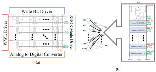
Figure 2.
(a) Proposed XNOR-SRAM Architecture. (b) Single Neuron Calculation.
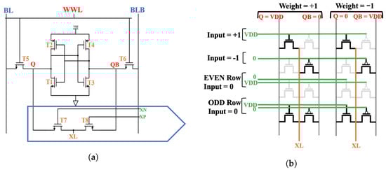
Figure 3.
(a) Proposed 8T XNOR-SRAM Bitcell (b) Transistor Behavior of the XNOR Mode.

Table 1.
Transistor size and ratio for bit cell configuration.
3.2. Proposed CIM Operation and Analysis
- Binary Weights and Binary Activations: For binary activations, the bit cell produces the XNOR dot-product output of (+1) once, with one strong PU by NMOS, and once with one strong PU by PMOS in two ways. The first is when the input is (+1), and the weight is (+1), and the second is when the input is (−1) and the weight is (−1), respectively. Firstly, the (XN) and (XP) inputs are high at VDD, and the weight stored in the Q node is also high at VDD. So, the XNOR dot-product output is generated by turning the NMOS transistor ON and, thus, driving the (XL) high to (VDD-Vth) via the Q node. Secondly, the (XN) and (XP) inputs are low at 0, and the weight stored in the Q node is also low at 0. So, the XNOR dot-product output is generated by turning the PMOS transistor ON and, thus, driving the (XL) high to (VDD-Vth) via the QB node. The bit cell produces the XNOR dot-product output of (−1) once with one strong PU by NMOS and once with a one strong PU by PMOS in two ways. The first is when the input is (+1), and the weight is (−1), and the second when the input is (−1), and the weight is (+1), respectively. Firstly, the (XN) and (XP) inputs are high at VDD, and the weight stored in the Q node is low at 0. So, the XNOR dot-product output is generated by turning the NMOS transistor ON, and thereby driving the voltage of (XL) to discharge. Secondly, the (XN) and (XP) inputs are low at 0, and the weight stored in the Q node is high at 1. So, the XNOR dot-product output is generated by turning the PMOS transistor ON, and thereby the voltage of (XL) is discharged via the QB node. This is described in rows 1–4 in Table 2, and shown in the first two rows in Figure 3b. From Table 2, it is shown that we represented the weight (+1) with (Q = VDD & Qb = 0) and we represented the Weight (−1) with (Q = 0 & Qb = VDD). For the input (+1) (XN & XP = VDD) and the input (−1) (XN & XP = 0). We presented the input (0) in two ways, either (XN = 0 & XP = VDD) or (XN = VDD & XP = 0).
Table 2. Logic map for the Product between the Input and the Weight.
- Binary Weights and Ternary Activations: To exhibit the ternary activations, we had to consider the input (activation) value of (0). For ternary activations, the bit cell produces the XNOR dot-product output of (0) in two ways. First, when the input is (0), and the weight is (+1), and second, when the activation is (0), and the weight is (−1). Now taking into consideration that the XNOR-output (0) did not contribute to the voltage of the XNOR line (XL), we still had to present it and perform the calculation of it. There are two ways to produce the XNOR dot-product output of (0). In the first method, we turned both transistors OFF by setting the inputs (XN) low at 0 and (XP) high at VDD, and we named this (0-even-rows). In the second method, we turned both transistors ON, and this was done to consider when the input combination of (XN) was high at VDD and (XP) low at 0, and we named this (0-odd-rows). We also assumed that the XNOR mode driver would distribute the input combinations of the XNOR (0) on the 255 rows evenly. This is described in rows 5–8 in Table 2, and shown in the last two rows in the Figure 3b.
- ADC Operation Description: As stated earlier, the design consisted of 256-bit cells in one column, and 64 cells for the dot-product operations. The ADC block in the design consisted of 32 cells for ADC reference and 32 cells for ADC calibration. The dot-product analog result obtained from the XL was quantized using a comparator ADC. We quantized our analog summation of the dot-product results using Equation (1) below, where N is the number of output bits. Thus, we needed 33 cycles for ADC. In 33 cycles for the ADC operation, where each cycle was an ADC reference, the cell values could be swept from (−32 to +32) for a step size of 2. The dot-product results were compared to the comparator ADC primary operation method as if the dot-product was less than the ADC reference value, it was quantized to 0, and if it was equal to, or larger than, the ADC reference value, it was quantized to 1.
4. Measurement Results
For reliable comparison and implementation, we used, for the XNOR-Mode in our proposed SRAM-CIM design, the minimum transistor size in the bit cell, and for the state-of-the-art [14], the minimum transistor size was used for everything except the transistors the authors pointed out that they used slightly bigger size. We also used the same capacitor size, voltage source, temperature, and test circuit. We used FreePDK45 nm technology for verification of the proposed structure and comparison, and the simulation was done via Synopsys Hspice, considering the power consumption and speed (Delay). Figure 4, Figure 5 and Figure 6 were obtained via Cosmoscope. Table 3 and Table 4. below are the power consumption and the delay results obtained for our one bit cell dot-product proposed design structure compared with the state-of-the-art one bit cell structure.
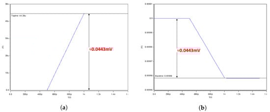
Figure 4.
Charging or Discharging range with a single SRAM bit cell (0.0443 mV). (a) Charging range for +1 result. (b) Discharging range for −1 result.
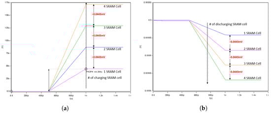
Figure 5.
Charging or Discharging range with 4× SRAM bitcells. (a) Charge range for up to +4 result. (b) Discharge range for up to −4 result.
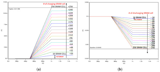
Figure 6.
Charging or Discharging range with 256× SRAM bitcells. (a) Charge range for up to +256 result. (b) Discharge range for up to −256 result.
Table 3.
Results for Power Consumption.
Table 4.
Results for Delay.
The power consumption comparison results showed an improvement from a minimum of 30%, for the case of Input (+1) & Weight (+1), up to 98% for the case of Input (0) & Weight (+1). This superior improvement for this case came from the fact that both transistors (T7 & T8) were OFF, and, as stated earlier, this was because the dot-product output 0 did not contribute (add) to the voltage value of the XNOR line (XL).
The delay between our proposed design and the state-of-the-art showed an improvement that ranged from a minimum of 30–90%. This arose from the fact that the number of transistors used in our bit cell was less than the number used in the state-of-the-art (8 vs. 12). In every case for the state-of-the-art design, 10 Transistors were ON at the same time, while in our design we had seven transistors ON in every case, except the case when both transistors T7 and T8 were OFF, when we had 6 transistors ON.
In our column-based neuron design, the charging and discharging level in the XNOR-Line (XL) for a single SRAM cell was set in the range of 0.0441–0.0446 mV, or an average of 0.0443 mV, as shown in Figure 4a,b respectively. Figure 4a shows the charging of a single SRAM cell and, hence, the XL was rising from the reference point (0.0 V). Figure 4b shows the discharging of a single SRAM cell and, hence, the XL was falling from the reference point (0.9 V). The linearity of the accumulated work increased or decreased according to the number of SRAM cells (i.e., if four SRAM cells were discharged, the XL discharge level became 0.0443 × 4 = 0.1772 mV). This is shown in Figure 5a,b respectively, where Figure 5a shows the charging of the XL of four SRAM cells, and Figure 5b shows the discharging of the XL of four SRAM cells. In other words, in our column-based design, the cell’s charging or discharging result accumulated in the XL to sum the multiplier (input × weight) result in each cell into one neuron value. We applied 0.9 V as VDD for all the bit cells to maintain the result’s linearity and support low power designs.
Figure 6a,b show the accumulation results of the multiplication results. Since our CIM had a total of 256× inputs from X[0] to X[255], the maximum value of the sum of binary multiplication results could be +256 or −256. Moreover, the charging and discharging range of a single cell ranged between 0.0441–0.0456 mV, or an average of (0.0443 mV), which could indicate −1, 0, or +1. Therefore, the sum of the multiplication results of 256× cells was 0.0443 mV × 256 = 0.0113 V, which could be charged or discharged at the reference point (0.90 V) to represent the +256 or −256. In other words, a value of −256 could be expressed as (0.90 V − 0.0113 V = 0.8887 V), and a value of +256 could be expressed as (0.0 V + 0.01141 V = 0.01141 V). The results are simulated in detail in Figure 6a,b, and it could be confirmed that our results maintained the linearity of the accumulated work.
5. Conclusions
In this paper, we proposed a novel 8T SRAM-based ultra-low-power compute-in memory (CIM) design, that directly supports XNOR-Net and TBN DNNs. To compute the vector–matrix multiplication of the ternary inputs and binary weights DNNs, we added two extra transistors to the conventional 6T SRAM structure to perform the XNOR dot-product between the inputs and the weights already stored in the bit cell. The accumulation was done by adding all the voltages from the shared XNOR line (XL) in the one column between all the cells. After that, this Analog XL was then transformed into the Digital format via the ADC. Our proposed design results showed a maximum of 98% improvement against the state-of-the-art [14] in terms of the power consumption, and up to 90% in terms of delay.
Author Contributions
Conceptualization, Data curation, Formal analysis, Investigation, Methodology, Validation, N.A.; Writing—original draft, Writing—review and editing, Y.K., J.C. and K.K.C.; Supervision, Funding acquisition, Project administration, K.K.C. All authors read and agreed to the published version of the manuscript.
Funding
This work was supported by the Technology Innovation Program of the Ministry of Trade, Industry & Energy (MOTIE, Republic of Korea). [#1415181272, Software and Hardware Development of cooperative autonomous driving control platform for commercial special and work-assist vehicles].
Acknowledgments
We thank our colleagues from KETI and KEIT, who provided insight and expertise that greatly assisted the research and greatly improved the manuscript.
Conflicts of Interest
The authors declare no conflict of interest.
Abbreviations
The following abbreviations were used in this manuscript:
| SRAM | Static Random-Access Memory |
| eNVM | Embedded-non-Volatile-Memory |
| CIM | Compute-In-Memory |
| ADC | Analog to Digital Converter |
| TBN | Ternary Binary Neural Networks |
| MAC | Multiply-And-Accumulate |
| VMM | Vector-Matrix Multiplication |
| GPU | Graphical Processing Unit |
| TPU | Tensor Processing Unit |
| SET | Single-event Transient |
| DNU | Double-node Upset |
References
- Hinton, G.; Deng, L.; Yu, D.; Dahl, G.E.; Mohamed, A.-R.; Jaitly, N.; Senior, A.; Vanhoucke, V.; Nguyen, P.; Sainath, T.N.; et al. Deep neural networks for acoustic modeling in speech recognition: The shared views of four research groups. IEEE Signal Process. Mag. 2012, 29, 82–97. [Google Scholar] [CrossRef]
- Taigman, Y.; Yang, M.; Ranzato, M.A.; Wolf, L. DeepFace: Closing the gap to human-level performance in face verification. In Proceedings of the IEEE Conference on Computer Vision and Pattern Recognition, Columbus, OH, USA, 24–27 June 2014; pp. 1701–1708. [Google Scholar]
- Fang, W.; Wang, L.; Ren, P. Tinier-YOLO: A Real-Time Object Detection Method for Constrained Environments. IEEE Access 2020, 8, 1935–1944. [Google Scholar] [CrossRef]
- Sze, V.; Chen, Y.-H.; Yang, T.-J.; Emer, J.S. Efficient Processing of Deep Neural Networks: A Tutorial and Survey. Proc. IEEE 2017, 105, 2295–2329. [Google Scholar] [CrossRef]
- Chan, T.-H.; Jia, K.; Gao, S.; Lu, J.; Zeng, Z.; Ma, Y. PCANet: A Simple Deep Learning Baseline for Image Classification? IEEE Trans. Image Process. 2015, 24, 5017–5032. [Google Scholar] [CrossRef] [PubMed]
- Abdel-Hamid, O.; Mohamed, A.-R.; Jiang, H.; Deng, L.; Penn, G.; Yu, D. Convolutional Neural Networks for Speech Recognition. Proc. IEEE/ACM Trans. Audio Speech Lang. Process. 2014, 22, 1533–1545. [Google Scholar] [CrossRef]
- Rastegari, M.; Ordonez, V.; Redmon, J.; Farhadi, A. XNOR-Net: ImageNet classification using binary convolutional neural networks. In European Conference on Computer Vision; Springer International Publishing: Cham, Switzerland, 2016. [Google Scholar]
- Wan, D.; Shen, F.; Liu, L.; Zhu, F.; Qin, J.; Shao, L.; Shen, H.T. TBN: Convolutional Neural Network with Ternary Inputs and Binary Weights. In Proceedings of the European Conference on Computer Vision (ECCV), Munich, Germany, 8–14 September 2018. [Google Scholar]
- Song, T.; Jung, J.; Rim, W.; Kim, H.; Kim, Y.; Park, C.; Do, J.; Park, S.; Cho, S.; Jung, H.; et al. A 7nm FinFET SRAM using EUV lithography with dual writedriver-assist circuitry for low-voltage applications. In Proceedings of the IEEE International SolidState Circuits Conference (ISSCC), San Francisco, CA, USA, 11–15 February 2018. [Google Scholar]
- Yu, S.; Jiang, H.; Huang, S.; Peng, X.; Lu, A. Compute-in-Memory Chips for Deep Learning: Recent Trends and Prospects. IEEE Circuits Syst. Mag. 2021, 21, 31–56. [Google Scholar] [CrossRef]
- Yan, A.; Zhou, J.; Hu, Y.; Cui, J.; Huang, Z.; Girard, P.; Wen, X. Novel Quadruple Cross-Coupled Memory Cell Designs with Protection Against Single Event Upsets and Double-Node Upsets. IEEE Access 2019, 7, 176188–176196. [Google Scholar] [CrossRef]
- Lu, A.; Peng, X.; Luo, Y.; Yu, S. Benchmark of the compute-inmemory based DNN accelerator with area constraint. IEEE Trans. VLSI Syst. 2020, 28, 1945–1952. [Google Scholar] [CrossRef]
- Si, X.; Khwa, W.-S.; Chen, J.-J.; Li, J.-F.; Sun, X.; Liu, R.; Yu, S.; Yamauchi, H.; Li, Q.; Chang, M.-F. A Dual-Split 6T SRAM-Based Computing-in-Memory Unit-Macro With Fully Parallel Product-Sum Operation for Binarized DNN Edge Processors. IEEE Trans. Circuits Syst. I Regul. Pap. 2019, 66, 4172–4185. [Google Scholar] [CrossRef]
- Yin, S.; Jiang, Z.; Seo, J.-S.; Seok, M. XNOR-SRAM: In-Memory Computing SRAM Macro for Binary/Ternary Deep Neural Networks. IEEE J. Solid State Circuits 2020, 55, 1733–1743. [Google Scholar] [CrossRef]
- Biswas, A.; Chandrakasan, A.P. CONV-SRAM: An Energy-Efficient SRAM With In-Memory Dot-Product Computation for Low-Power Convolutional Neural Networks. IEEE J. Solid State Circuits 2019, 54, 217–230. [Google Scholar] [CrossRef]
Disclaimer/Publisher’s Note: The statements, opinions and data contained in all publications are solely those of the individual author(s) and contributor(s) and not of MDPI and/or the editor(s). MDPI and/or the editor(s) disclaim responsibility for any injury to people or property resulting from any ideas, methods, instructions or products referred to in the content. |
© 2023 by the authors. Licensee MDPI, Basel, Switzerland. This article is an open access article distributed under the terms and conditions of the Creative Commons Attribution (CC BY) license (https://creativecommons.org/licenses/by/4.0/).