Article

A Kind of Optoelectronic Memristor Model and Its Applications in Multi-Valued Logic

1
School of Electronics and Information, Hangzhou Dianzi University, Hangzhou 310018, China
2
College of Electrical Engineering, Zhejiang University, Hangzhou 310027, China
3
Zhejiang Provincial Key Lab of Equipment Electronics, Hangzhou 310018, China
*
Authors to whom correspondence should be addressed.
Electronics 2023, 12(3), 646; https://doi.org/10.3390/electronics12030646
Submission received: 21 December 2022 / Revised: 15 January 2023 / Accepted: 25 January 2023 / Published: 28 January 2023
(This article belongs to the Special Issue Memristive Devices and Systems: Modelling, Properties & Applications)

Abstract

:
Memristors have been proved effective in intelligent computing systems owing to the advantages of non-volatility, nanometer size, low power consumption, compatibility with traditional CMOS technology, and rapid resistance transformation. In recent years, considerable work has been devoted to the question of how to design and optimize memristor models with different structures and physical mechanisms. Despite the fact that the optoelectronic effect inevitably makes the modelling process more complex and challenging, relatively few research works are dedicated to optoelectronic memristor modelling. Based on this, this paper develops an optoelectronic memristor model (containing mathematical model and circuit model). Moreover, the composite memristor circuit (series- and parallel-connected configuration) with a rotation mechanism is discussed. Further, a multi-valued logic circuit is designed, which is capable of performing multiple logic functions from 0–1, verifying the validity and effectiveness of the established memristor model, as well as opening up a new path for the circuit implementation of fuzzy logic.

1. Introduction

Memristors that are non-volatile and nano-sized, and that have low power consumption, compatibility with conventional CMOS technology, and variable resistance have been widely used in intelligent computing systems [1,2,3,4,5]. This novel circuit component, was first proposed by Chua L in 1971, represents the relationship between charge and flux [6]. The existence of a physical memristor was first verified by Hewlett-Packard Lab in 2008, and it was confirmed to be a nanoscale passive two-terminal circuit component [7]. The successful preparation of memristors has attracted a lot of attention among research scholars around the world, and numerous memristor devices with different structures and physical mechanisms have been prepared [8,9,10].
Owing to stringent manufacturing processes and high costs, actual memristors are difficult to prepare outside the laboratory [11,12,13]. Considerable work has been devoted to the study of mathematical and circuit models that can reproduce the complex dynamics of memristors, such as the HP model [14], the spintronic model [15], the threshold adaptive model (TEAM) [16], the voltage threshold adaptive model (VTEAM) [17], etc. However, the present modelling is mostly based on two factors: the voltage applied to the memristor and the current flowing through it, which cannot accommodate the physical memristor properties prepared with evolving materials [18,19,20]. Indeed, physical memristors are affected by multiple factors such as light, temperature, humidity, and magnetic field, increasing the complexity and difficulty of modelling [21,22,23,24], and relatively little and incomplete work has been done in this area. In order to approximate the electrical characteristics possessed by physical amnesic resistors, this paper develops a model for optoelectronic memristors affected by both optical and electrical signals.
With the exploration of the binary characteristics of memristors, the application of memristors in logic circuits has received a lot of attention [25,26,27,28]. Existing research in the field of memristor-based logic implementation is mainly aimed at binary logic (e.g., material implication, memristor-aided logic, and memristor-ratioed logic), and ternary logic (e.g., balanced ternary logic and unbalanced ternary logic) [29,30,31,32,33]. However, relatively little research has been conducted on the implementation of multi-valued logic circuits based on memristors. Multi-valued logic with more logic states is an extension of traditional binary (or ternary) logic, which has only two (or three) logical states. Compared with binary (or ternary) logic, multi-valued logic carries more information in the process of processing a large amount of data, and has a faster operational speed, smaller area and size, and lower power consumption [34,35,36]. This paper presents the design of a multivalued logic circuit based on the established optoelectronic model. The research gaps and the main contributions of this paper are summarized in Table 1.
The rest of the paper is organized as follows. Section 2 details the mathematical and PSIPCE models of a kind of optoelectronic memristor. Moreover, a series of tests and analysis on the electrical characteristics of the model is carried out in the same section. Section 3 discusses a composite circuit incorporating a rotation mechanism and proposes a multivalued logic circuit based on this circuit. The section concludes with a series of simulation experiments and analysis to verify the correctness of the proposed multi-valued logic and the validity of the model. Section 4 discusses the limitations of the designed multi-valued logic circuit and provides future research directions. Finally, Section 5 summarizes the whole work.

2. Optoelectronic Memristor Model and Electrical Characteristics Analysis

2.1. Background of Opoelectronic Memristor

Before modeling the optoelectronic memristor, the background of the optoelectronic memristor is studied in terms of both device structure and operating principles, which leads to a better understanding of the optoelectronic effects that affect the electrical characteristics of the memristor.
The modeled optoelectronic memristor device is prepared from ITO/MgO/HfO2/ITO material, where two layers of transparent conductive oxide ITO are used as the top electrode (TE) and bottom electrode (BE) of the device [21]. The wide bandwidth oxide (MgO/HfO2) introduces the optical functionality in the resistive switching device while maintaining the optical transparency, and the MgO layer increases the durability, retention performance, and resistive ON/OFF ratio of the device. The specific device structure is shown in Figure 1a.
The working principle of the device is illustrated in Figure 1b, and it can be discussed in three cases depending on the voltage and light illumination. When a positive voltage is applied at the TE terminal and the BE terminal is grounded, the positive voltage induces the breakage of the Hf-O and Mg-O bonds, and a large number of oxygen vacancies (VO) and oxygen ions (O2−) are formed. Conductive filaments (CF) are formed inside the device, which causes the device to switch from a high resistance state (HRS) to a low resistance state (LRS). Owing to the larger amount of energy required to form VO from MgO, most of the VO during the setting process is produced by HfO2. Notably, O2− is not stacked near the TE interface, but at the intersection of MgO and HfO2.
In the case that a negative voltage is applied at the TE terminal and the BE terminal is kept grounded, O2− will recombine with VO to form oxygen atoms under the negative voltage, leading to the rupture of CF. Further, the current is reset and the resistance state of the device is transformed to HRS.
In addition, the device is influenced by optical factors as well as electrical stimulation. The illumination is able to provide energy to O2−, which in turn promotes O2− and VO to achieve recombination. The effects of illumination and negative voltage on the electrical characteristics of the device are similar, and both achieve the reset function.

2.2. Modelling of Opoelectronic Memristor

In order to facilitate subsequent studies on the application of the optoelectronic memristor, the device is modeled by improving the VTEAM modelling method and employing the optoelectronic effect. Its resistance can be represented by the following mathematical equation.
M ( x ) = R on + R off R on x off x on ( x x on )
where M denotes the resistance of the optoelectronic memristor, which is limited to [Ron, Roff]. x is the state variable, with maximum and minimum values of xon and xoff, and the dynamic function of x can be described by the following equation.
d x d t = { [ k on ( V ( t ) V th 1 1 ) α on + I p ε I p max ] f ( x ) , 0 < V th 1 V ( t ) I p ε I p max f ( x ) , V th 2 < V ( t ) V th 1 [ k off ( V ( t ) V th 2 1 ) α off + I p ε I p max ] f ( x ) , V ( t ) V th 2 < 0
f ( x ) = 1 ( β x 1 ) 2 p
where kon(V(t)/Vth1 − 1)αon and koff(V(t)/Vth2 − 1)αoff are electrical effect simulation terms that achieve not only a decrease in resistance when a positive voltage is applied, but also an increase in resistance for negative voltages. kon, koff, αon, and αoff are all fitting parameters of the model, Vth1 and Vth2 denote the positive and negative threshold voltage, respectively. V(t) represents the voltage loaded onto the memristor. Ip/(εIpmax) is the light effect simulation term to realize the function of increasing the memristance upon illumination. ε denotes the parameter capable of regulating the effect of light and Ipmax is the maximum illumination power intensity. Ip indicates the optical power intensity applied to the memristor. f(x) acts as a window function for binding x to [xon, xoff]. β and p are fitting parameters of the model.
Accordingly, a SPICE model of optoelectronic memristor is proposed to perform the subsequent circuit simulation. The specific sub-circuit description is shown in Table 2.
To evaluate the accuracy of the proposed model, we fit the model based on real experimental data, as shown in Figure 2. Figure 2a shows the IV curve of the memristor in the dark environment, where the black ball indicates the real experimental data and the red solid line indicates the fitting result of the model. Notably, the memristor is initialized to a high resistance state before conducting this experiment. Figure 2b shows the IV curves of the memristor before and after applying illumination to it, where the blue and black lines with triangles indicate the real experimental data pre- and post-illumination, respectively, and the gray and red lines show the fitting results pre- and post-illumination, respectively. Notably, the resistance of the initialized memristor is a lower resistance before carrying out this experiment and the illumination is white light (390–780 nm) with an optical power intensity of 100 W/m2.
From Figure 2, the established memristor model has a good overlap with the actual memristor electrical characteristic curve. Root mean square error (RMSE) is introduced as an indicator for objective analysis, and its mathematical expression is shown below:
RMSE = 1 n ( i = 1 n ( V real , i V fit , i ) 2 V fit 2 + i = 1 n ( I real , i I fit , i ) 2 I fit 2 )
where n is the number of samples, Vreal,i and Ireal,i the voltage and current on the memristor during the testing process, and Vfit,i and Ifit,i represent the voltage and current on the model during the fitting process. Vfit and Ifit denote the Euclidean criterion for the voltage and current of the memristor model. Normally, a smaller RMSE represents a better fit.
From Figure 2a, the model can achieve the electrical setting function under positive voltage, where the model can be fitted to the measured data points with the RMSE value of 1.13%. As shown in Figure 2b, the simulated I-V curves are matched with the I-V curves in the pre- and post-illumination periods with RMSE values of 1.65% and 1.98%, respectively. When illumination is applied, the resistance of the memristor increases and the current flowing through the memristor decreases. In general, the fitting results show that the constructed optoelectronic memristor model is capable of characterizing the performance of the ITO/MgO/HfO2/ITO memristor.

2.3. Electrical Characteristics Analysis

To demonstrate the electrical characteristics of the proposed optoelectronic memristor model, a series of tests and analysis circuit simulations are performed, and the experimental results are shown in Figure 3, Figure 4 and Figure 5. The specific parameters of the memristor model are detailed in Table 2 and Table 3. Notably, the experiments are conducted on a desktop workstation equipped with Core i7-10700 processor, 32 GB RAM and Windows 10 operating system using Matlab2018 and PSpice software.
Figure 3 illustrates the electrical characteristics (volt-ampere characteristics and memristance variation rule) of the memristor under different illumination conditions. The relationship between the current flowing through the memristor model and the applied voltage is shown in Figure 3a,c, and the variation of memristance with time is shown in Figure 3b,d.
The IV characteristic curves in Figure 3a,c both show squeezed hysteresis curves at the origin, which demonstrates that the proposed memristor model conforms to the definition of a generalized memristor [37]. Notably, the model is relatively symmetrical in the positive and negative voltage regions under the condition of no illumination, whereas the area of the pinched hysteresis loop in the negative voltage region is greatly reduced upon optical stimulation, and the positive and negative regions are asymmetric. This occurs because the light stimulus increases the memristance as well as the negative voltage, weakening the effect of the negative voltage on the electrical properties of the model.
From Figure 3b, it can be observed that the electrical characteristics of this memristor model are similar to those of the VTEAM model under conditions without illumination, and the variation of its resistance with time can be described in five stages. In stage 1, the resistance keeps Roff constant when the scanning voltage increases from 0 V to Vth1; in stage 2, the resistance decreases from Roff to Ron when applying the voltage to the memristor over Vth1; in stage 3, the resistance remains unchanged as the scanning voltage decreases from Vth1 to Vth2; in stage 4, when the voltage is less than Vth2, the memristor transforms from the LRS to the HRS; and in stage 5, by the time the voltage increases from Vth2 to 0 V, the resistance characteristics are the same as in stages 1 and 3, and the HRS is maintained. Comparing Figure 3b,d, it can be found that the optical stimulation causes an alteration of the resistance variation rule in stage 3, which is the time interval from 76.91 ns to 123.2 ns. The inclusion of the optical stimulus leads to the reversal of the soft breakdown, causing an increase in the resistance of the memristor. Notably, with the low power density of the applied optical signal here, the optical stimulus has less effect on the electrical characteristics of the memristor in comparison with the electrical stimulus and does not lead to a shift in the resistance variation pattern in the remaining phases.
Figure 4 shows the results of the effect of optical stimulation with different irradiation power densities and constant voltage of different amplitudes on the variation pattern of the memristance. Figure 4a–c shows the memristor response curves upon the application of electrical stimuli of 3 V, 0 V and −3 V to the memristor model with the initial resistance Ron within the time interval [0, 300]ns at different optical power densities (i.e., 10, 50, 100, 200, 300, and 500 W/m2), respectively. Considering that the resistance state of the memristor with initial resistance Roff will not change with external electrical stimuli of −3 V and 0 V, thus only the effect of different optical power densities on the memristance under 3 V positive voltage is simulated. From Figure 4a,b, it is obvious that the higher the optical power density, the faster the rate of resistance enhancement. A summary analysis of Figure 4c,d shows that a sufficiently large optical stimulus can surpass the effect of positive voltage on the electrical characteristics of the memristor. Notably, the green, yellow, blue and red lines in Figure 4c are overlapped, and the purple and brown lines in Figure 4d are overlapped.
Figure 5 depicts the electrical characteristic curves of the memristor composite circuit (series- and parallel-connected configuration) at an optical power density of 100 W/m2. Figure 5a,c,e illustrates the resistance variation curves of two optoelectronic memristors with the same initial resistance connected in series at −5 V, 0 V and 5 V electrical stimuli, respectively, while Figure 5b,d,f represents the resistance variation curves connected in parallel.
From Figure 5, since the model parameters (including the initial memristances) of the two memristors are the same, the corresponding resistance variation pattern (which can be referred to the resistance variation pattern in Figure 3d) is also the same, as shown in the overlapping of the red dashed line and the orange solid line. When two memristors are connected in series in the same direction, the resistance state of both memristors changes to the HRS under the combined effect of negative voltage and illumination, as shown in Figure 5a. In the case of illumination separately, as shown in Figure 5c, the resistances of both memristors also increase to Roff. Notably, compared to Figure 5a, the change (growth) curve of the resistance is relatively smooth owing to the lack of the effect of the negative voltage. Under the effect of positive voltage, as shown in Figure 5e, the resistance of both memristors decreases owing to the lower power density of illumination radiation, whose effect on the optoelectronic memristors is smaller than that of positive voltage. In addition, when two memristors are connected in parallel in the same direction, as shown in Figure 5b,d,f, the resistance variation trend of the two memristors is the same as that in series in the same direction. However, when the same voltage is applied to the input, the voltage divided by the parallel memristors is larger, so the rate of resistance variation is relatively faster. Moreover, the equivalent resistance Mtotal of the series circuit is calculated as the sum of the resistance M1 and M2, i.e., Mtotal = M1 + M2, and the equivalent resistance of the parallel circuit satisfies: Mtotal = M1M2/(M1 + M2).

3. Rotation Mechanism Based Multi-Valued Logic

In this section, a composite memristor circuit (series- and parallel-connected configuration) incorporating a rotation mechanism is discussed. According to the composite circuit, a circuit capable of implementing 0–1 multiple logic functions is subsequently proposed. The specific operation procedure and simulation results are described as follows.

3.1. Rotation Mechanism Based Composite Circuit

The schematic diagram of the composite memristor circuit based on the rotation mechanism is depicted in Figure 6, where A, B, C are the ports of the connection line, and port B is the center of rotation. The rotation mechanism enables the conversion of series and parallel configuration circuits, and the circuit during the conversion contains an intermediate state in addition to the series and parallel states.

3.2. Implementation of Multi-Valued Logic

Incorporating the composite circuit based on the rotation mechanism, a circuit for implementing multi-valued logic is designed (as illustrated in Figure 7). Note that the proposed circuit contains two valid states during rotation, i.e., state I and state II.
The memristors (Ms1, Ms2, and Ms3) employed in the circuit are the proposed optoelectronic memristors, whose resistances (Rs1, Rs2, and Rs3) are varied in [Ron, Roff] by the joint effect of electrical and optical stimulation. The input voltages (A1 and A2) and the optical power densities (B1, B2, and B3) are the input state variables of the circuit. R is the regular resistor, and the voltage (Vout1 and Vout2) across it indicates the output state variable of the logic circuit.
Before executing the multi-valued logic operation, the memristor Ms1, Ms2, and Ms3 are required to be initialized to their lowest value Ron. The specific process of implementing multiple logic functions from 0 to 1 for the two states is described as follows.

3.2.1. State I for Multi-Valued Logic

For multi-valued logic operation, the electrical inputs (A1 and A2) always have two states Von and Voff, representing the logic “1” and logic “0”, respectively. Notably, the value of voltage Voff used in this section is 0 V. According to the principle of series voltage division and parallel current division, the node voltage Vout1 can be calculated with the following equation.
V out 1 = { 0 A 1 = V off , A 2 = V off R R + R s 1 / / ( R s 2 + R s 3 ) V on A 1 = V on , A 2 = V on R / / R s 1 R / / R s 1 + ( R s 2 + R s 3 ) V on A 1 = V off , A 2 = V on R / / ( R s 2 + R s 3 ) R / / ( R s 2 + R s 3 ) + R s 1 V on A 1 = V on , A 2 = V off
When A1 = A2 = Voff, the node voltage Vout1 is always 0 V, independent of whether the state of the memristor is changed or not, thus the case is not described when the optical stimulus is applied to the memristor. The optical inputs (B1, B2, and B3), which always have two states Iph and Ipl, representing the logic “1” and logic “0”, respectively, can be discussed in the following six cases.
  • Case A: When B1 = B2 = B3 = Ipl, the node voltage Vout1 can be computed as:
V out 1 = { R R + R on / / 2 R on V on A 1 = V on , A 2 = V on R / / R on R / / R on + 2 R on V on A 1 = V off , A 2 = V on R / / 2 R on R / / 2 R on + R on V on A 1 = V on , A 2 = V off
According to the resistance variation pattern of optoelectrical memristor, the low optical power density is not sufficient to trigger a change in the resistance of the optoelectrical memristor, thus the resistance of memristors (Rs1, Rs2, and Rs3) remains in the initial Ron.
  • Case B: When B1 = Ipl, B2 = Ipl and B3 = Iph (or B1 = Ipl, B2 = Iph and B3 = Ipl), the node voltage Vout1 can be computed as:
V out 1 = { R R + R on / / ( R on + R off ) V on A 1 = V on , A 2 = V on R / / R on R / / R on + R on + R off V on A 1 = V off , A 2 = V on R / / ( R on + R off ) R / / ( R on + R off ) + R on V on A 1 = V on , A 2 = V off
Here, the high optical power density has a greater effect on the resistance variation of the memristor than the positive voltage, with the memristance of Rs3 or Rs2 increasing from Ron to Roff. The memristors Ms1 and Ms2 (or Ms1 and Ms3) remain in the low resistance state.
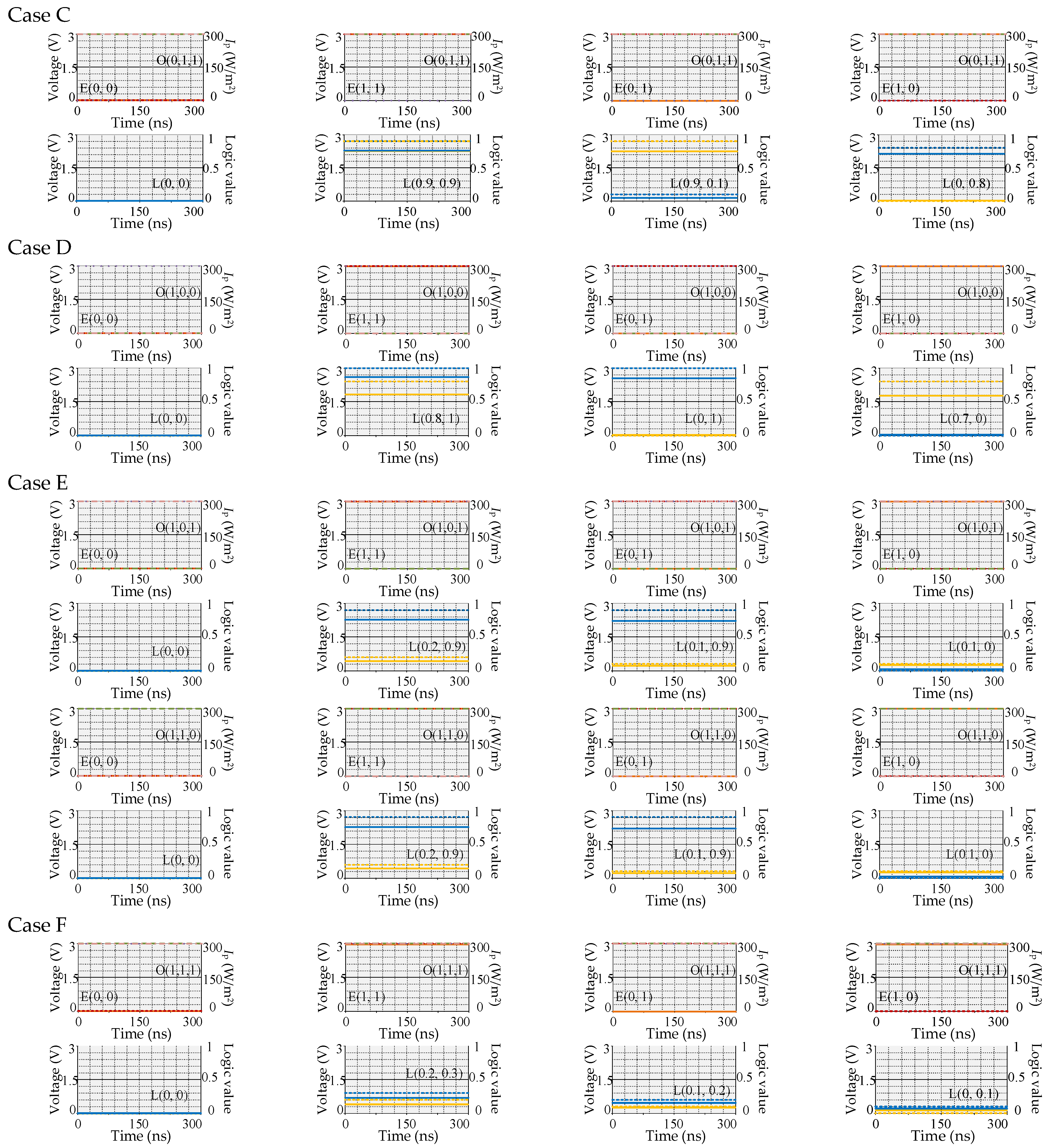
  • Case C: When B1 = Ipl and B2 = B3 = Iph, the node voltage Vout1 can be computed as:
V out 1 = { R R + R on / / 2 R off V on A 1 = V on , A 2 = V on R / / R on R / / R on + 2 R off V on A 1 = V off , A 2 = V on R / / 2 R off R / / 2 R off + R on V on A 1 = V on , A 2 = V off
Here, the memristor Ms1 remains in the initial low resistance state, and the resistances of Ms2 and Ms3 increase to the highest value Roff.
  • Case D: When B1 = Iph and B2 = B3 = Ipl, the node voltage Vout1 can be computed as:
V out 1 = { R R + R off / / 2 R on V on A 1 = V on , A 2 = V on R / / R off R / / R off + 2 R on V on A 1 = V off , A 2 = V on R / / 2 R on R / / 2 R on + R off V on A 1 = V on , A 2 = V off
Here, the memristors Ms2 and Ms3 remain in the initial low resistance state, and the resistance of Ms1 increases to the highest value Roff.
  • Case E: When B1 = Iph, B2 = Ipl and B3 = Iph (or B1 = Iph, B2 = Iph and B3 = Ipl), the node voltage Vout1 can be computed as:
V out 1 = { R R + R off / / ( R on + R off ) V on A 1 = V on , A 2 = V on R / / R off R / / R off + R on + R off V on A 1 = V off , A 2 = V on R / / ( R on + R off ) R / / ( R on + R off ) + R off V on A 1 = V on , A 2 = V off
Here, the memristors Ms2 (or Ms3) remain in the initial low resistance state, and the resistance of Ms1 and Ms3 (or Ms2) increase to the highest value Roff.
  • Case F: When B1 = B2 = B3 = Iph, the node voltage Vout1 can be computed as:
V out 1 = { R R + R off / / 2 R off V on A 1 = V on , A 2 = V on R / / R off R / / R off + 2 R off V on A 1 = V off , A 2 = V on R / / 2 R off R / / 2 R off + R off V on A 1 = V on , A 2 = V off
Here, the memristors Ms1, Ms2 and Ms3 shift to the high resistance state, and correspondingly all the memrsistances (Rs1, Rs2, and Rs3) increase to the highest value Roff.
The node voltage Vout1 in Case A is defined as logic “1” when the electrical inputs A1 = A2 = Von, and the output logic value for the rest of the cases is the ratio between the output Vout1 and the voltage corresponding to logic “1”. Assuming Roff ≥ 10 R, R ≅ 3 Ron, the truth table of state I for multi-valued logic is shown in Table 4.

3.2.2. State II for Multi-Valued Logic

The memristors Ms1 and Ms2 are rotated from series to parallel in state I, and the computational equation for the node voltage Vout2 is replaced as follows:
V out 1 = { 0 A 1 = V off , A 2 = V off R R + R s 1 / / ( R s 2 / / R s 3 ) V on A 1 = V on , A 2 = V on R / / R s 1 R / / R s 1 + ( R s 2 / / R s 3 ) V on A 1 = V off , A 2 = V on R / / ( R s 2 / / R s 3 ) R / / ( R s 2 / / R s 3 ) + R s 1 V on A 1 = V on , A 2 = V off
In the same way as state I, which implements multi-valued logic, the node voltage Vout2 can be further specified into the following six cases according to the optical inputs.
  • Case A: When B1 = B2 = B3 = Ipl, the variation of resistance Rs1, Rs2, and Rs3 is the same as that of Case A in state I, thus the node voltage Vout2 can be computed as:
V out 2 = { R R + R on / / ( R on / / R on ) V on V 1 = V on , V 2 = V on R / / ( R on / / R on ) R / / ( R on / / R on ) + R on V on V 1 = V off , V 2 = V on R / / R on R / / R on + R on / / R on V on V 1 = V on , V 2 = V off
  • Case B: When B1 = Ipl, B2 = Ipl and B3 = Iph (or B1 = Ipl, B2 = Iph and B3 = Ipl), the variation of resistance Rs1, Rs2, and Rs3 is the same as that of Case B in state I, thus the node voltage Vout2 can be computed as:
V out 2 = { R R + R on / / ( R on / / R off ) V on V 1 = V on , V 2 = V on R / / ( R on / / R off ) R / / ( R on / / R off ) + R on V on V 1 = V off , V 2 = V on R / / R on R / / R on + R off / / R on V on V 1 = V on , V 2 = V off
  • Case C: When B1 = Ipl and B2 = B3 = Iph, the variation of resistance Rs1, Rs2, and Rs3 is the same as that of Case C in state I, thus the node voltage Vout2 can be computed as:
V out 2 = { R R + R on / / ( R off / / R off ) V on V 1 = V on , V 2 = V on R / / ( R off / / R off ) R / / ( R off / / R off ) + R on V on V 1 = V off , V 2 = V on R / / R on R / / R on + R off / / R off V on V 1 = V on , V 2 = V off
  • Case D: When B1 = Iph and B2 = B3 = Ipl, the variation of resistance Rs1, Rs2, and Rs3 is the same as that of Case D in state I, thus the node voltage Vout2 can be computed as:
V out 2 = { R R + R off / / ( R on / / R on ) V on V 1 = V on , V 2 = V on R / / ( R on / / R on ) R / / ( R on / / R on ) + R off V on V 1 = V off , V 2 = V on R / / R off R / / R off + R on / / R on V on V 1 = V on , V 2 = V off
  • Case E: When B1 = Iph, B2 = Ipl and B3 = Iph (or B1 = Iph, B2 = Iph and B3 = Ipl), the variation of resistance Rs1, Rs2, and Rs3 is the same as that of Case E in state I, thus the node voltage Vout2 can be computed as:
V out 2 = { R R + R off / / ( R on / / R off ) V on V 1 = V on , V 2 = V on R / / ( R on / / R off ) R / / ( R on / / R off ) + R off V on V 1 = V off , V 2 = V on R / / R off R / / R off + R off / / R on V on V 1 = V on , V 2 = V off
  • Case F: When B1 = B2 = B3 = Iph, the variation of resistance Rs1, Rs2, and Rs3 is the same as that of Case F in state I, thus the node voltage Vout2 can be computed as:
V out 2 = { R R + R off / / ( R off / / R off ) V on V 1 = V on , V 2 = V on R / / ( R off / / R off ) R / / ( R off / / R off ) + R off V on V 1 = V off , V 2 = V on R / / R off R / / R off + R off / / R off V on V 1 = V on , V 2 = V off
As in the previous section, the ratio between the node voltage Vout2 and the voltage value Vout1 is defined as the corresponding output logic state variable. Assuming Roff ≥ 10 R, R ≅ 3 Ron, the correlation between the inputs (electrical inputs and optical inputs) and the output of state II is also shown in Table 4.
From Table 4, it can be shown that the proposed multi-valued logic circuit (including state I and state II) can implement 10 logic functions in 0–1. In addition, since the output state variables are voltages, the circuit is easy to cascade for implementing circuits with more complex functions.

3.3. Circuit Smulations and Analysis

To verify the effectiveness of the designed multi-valued logic circuit, a series of simulation experiments was performed on the same workstation as in the previous section. At the device level, the circuit uses three identical memristors, and the specific parameter configurations of the devices are detailed in Table 2. Notably, in addition to the memristors, the circuit needs to be configured with a resistor with a resistance of 0.3 kΩ, satisfying R = 3 Ron. At the circuit level, different input variables (the electrical input variables and the optical signal variables) are necessary for implementing the multi-valued logic, configuring Von = 3 V, Voff = 0 V, Iph = 300 W/m2, and Ipl = 0 W/m2.
Figure 8 shows the simulation results of the multi-valued logic circuit (including states I and II). A1 (the orange solid line) and A2 (the red dashed line) indicate the input electrical signals, which are represented in the figure as the first column E(0, 0), the second column E(1, 1), the third column E(0, 1), and the last column E(1, 0) for four electrical writing cases. B1 (the purple dotted line), B2 (the green dashed line), and B3 (the pink dashed line) indicate whether or not an optical signal is applied to the memristor, written by O(i, j, z), and correspond to the optical case in the previous section. Vout1 and Vout2 of state I and II are indicated by the yellow solid and the blue dashed lines, respectively. The logical state variables are represented by the yellow dashed and blue solid lines, respectively, denoted as L(m, n).
As in the theoretical analysis, the simulation results are classified into Case A–Case F depending on whether or not illumination is applied to the memristors. Under Case A, Case C, Case D, and Case F, the simulation results are further divided into four cases according to whether the voltage is applied at the input ports, corresponding to the first row, the fourth row, the fifth row, and the last row in Figure 8. In addition, Case B (Case E) contains two cases, B2 = Ipl, B3 = Iph and B2 = Iph, B3= Ipl, for which the simulation results in Figure 8 contain eight small diagrams. From the first column of Figure 8, the voltage is not available at the output regardless of whether there is a light input or not, which corresponds to logic “0”, since there is no voltage at the input. From Figure 8, the relationship between the input logic state variables and the output logic state variables obtained from the simulation corresponds to the truth table (Table 4), demonstrating that the circuit is capable of implementing multiple logic functions from 0–1, as well as verifying the validity of the constructed optoelectronic memristor model.
Then, the proposed multi-valued logic method is compared with five existing logic methods (i.e., material implication logic [29], memristor-aided logic [30], memristor ratioed logic [31], balanced ternary logic [32], and unbalanced ternary logic [33]). The comparison results including input variable, output variable, memristor type, computation form, need of resistors or transistors, initialization, cascading capacity and logic values are shown in Table 5.
In Table 5, the proposed logic method differs from the other five logic methods in terms of input logic state variables by adding illumination variables that can affect the electrical characteristics of the device. The proposed logic circuit is easy to cascade because light is accessible and the output logic state variable is voltage. The memristor-aided logic has the simplest circuit structure and requires no additional circuit components other than the memristors. However, this method is calculated in series as in material implication logic, and the calculation process is more complicated. The proposed method requires initialization compared to the memristor ratioed logic, which increases the operation cost. In addition, the proposed method is able to implement multi-valued logic, while the other methods are restricted to binary and ternary logic.

4. Discussion

Currently, most of the research in the field of memristor logic implementation is aimed at binary logic and ternary logic. Nevertheless, relatively little research has been done to implement multi-valued logic circuits based on memristors, and there are abundant opportunities and challenges. The proposed multi-valued logic circuit cannot implement “0.5” in logic 0–1, and the circuit structure will be further improved to achieve complete logic functions in the future. Since the discrete logic output of the designed circuit cannot realize the affiliation function, continuous logic output will be explored in the future to build fuzzy systems.

5. Conclusions

This paper focuses on the modelling method of optoelectronic memristors. Specifically, the mathematical and circuit models of the optoelectronic memristor are developed using the optoelectronic effect that affects the electrical characteristics of such devices. Notably, the modelling approach is based on an improvement of the popular VTEAM modelling method. Moreover, the electrical characteristics (referring to the volt-ampere characteristics and memristance variation rule) of a single memristor and its series-parallel circuit under different illumination conditions and different voltages are tested. Furthermore, a rotation mechanism is introduced to realize the conversion between series and parallel circuits, and a multi-valued logic circuit containing two states (state I and state II) is designed. Simulation results demonstrate that the designed circuit is capable of implementing 10 logic functions from 0–1, which verifies the effectiveness of the established optoelectronic memristor model as well as providing a new approach to the circuit implementation of fuzzy logic.

Author Contributions

Methodology, J.W.; software, Y.L. and C.H.; writing—original draft preparation, J.W. and S.Z.; conceptualization, J.W. and S.G.; writing—review and editing, J.W. and Y.L.; visualization, M.Y.; supervision, Y.Y.; funding acquisition, G.M. All authors have read and agreed to the published version of the manuscript.

Funding

This research was supported by G.M. and Y.Y., and it was funded by National Natural Science Foundation of China grant numbers 62001149 and 62001416, Fundamental Research Funds for the Provincial Universities of Zhejiang grant number GK229909299001-06, and Natural Science Foundation of Zhejiang Province grant number LQ21F010009.

Data Availability Statement

Not applicable.

Acknowledgments

The authors would like to thank the editorial board and reviewers for the improvement of this paper.

Conflicts of Interest

The authors declare no conflict of interest.

References

  1. Yang, X.; Taylor, B.; Wu, A.; Chen, Y.; Chua, L.O. Research progress on memristor: From synapses to computing systems. IEEE Trans. Circuits Syst. I: Regul. Pap. 2022, 69, 1845–1857. [Google Scholar] [CrossRef]
  2. Ji, X.; Dong, Z.; Lai, C.S.; Qi, D. A brain-inspired in-memory computing system for neuronal communication via memristive circuits. IEEE Commun. Mag. 2022, 60, 100–106. [Google Scholar] [CrossRef]
  3. Zhong, Y.; Tang, J.; Li, X.; Liang, X.; Liu, Z.; Li, Y.; Xi, Y.; Yao, P.; Hao, Z.; Gao, B.; et al. A memristor-based analogue reservoir computing system for real- time and power-efficient signal processing. Nat. Electron. 2022, 5, 672–681. [Google Scholar] [CrossRef]
  4. Zhong, Y.; Tang, J.; Li, X.; Gao, B.; Qian, H.; Wu, H. Dynamic memristor-based reservoir computing for high-efficiency temporal signal processing. Nat. Commun. 2021, 12, 1–9. [Google Scholar] [CrossRef] [PubMed]
  5. Dong, Z.; Ji, X.; Zhou, G.; Gao, M.; Qi, D. Multimodal neuromorphic sensory-processing system with memristor circuits for smart home applications. IEEE Trans. Ind. Appl. 2022. [Google Scholar] [CrossRef]
  6. Chua, L. Memristor-the missing circuit element. IEEE Trans. Circuit Theory 1971, 18, 507–519. [Google Scholar] [CrossRef]
  7. Strukov, D.B.; Snider, G.S.; Stewart, D.R.; Williams, R.S. The missing memristor found. Nature 2008, 453, 80–83. [Google Scholar] [CrossRef]
  8. Liao, K.; Lei, P.; Tu, M.; Luo, S.; Jiang, T.; Jie, W.; Hao, J. Memristor based on inorganic and organic two-dimensional materials: Mechanisms, performance, and synaptic applications. ACS Appl. Mater. 2021, 13, 32606–32623. [Google Scholar] [CrossRef]
  9. Dong, Z.; Ji, X.; Lai, C.S.; Qi, D.; Zhou, G.; Lai, L.L. Memristor-based hierarchical attention network for multimodal affective computing in mental health monitoring. IEEE Consum. Electr. Mag. 2022. [Google Scholar] [CrossRef]
  10. Shen, Z.; Zhao, C.; Zhao, T.; Xu, W.; Liu, Y.; Qi, Y.; Mitrovic, I.Z.; Yang, L.; Zhao, C.Z. Artificial synaptic performance with learning behavior for memristor fabricated with stacked solution-processed switching layers. ACS Appl. Electron. Mater. 2021, 3, 1288–1300. [Google Scholar] [CrossRef]
  11. Ji, X.; Lai, C.S.; Zhou, G.; Dong, Z.; Qi, D.; Lai, L.L. A flexible memristor model with electronic resistive switching memory behavior and its application in spiking neural network. IEEE Trans. Nanobioscience 2022, 22, 52–62. [Google Scholar] [CrossRef]
  12. Ji, X.; Dong, Z.; Lai, C.S.; Zhou, G.; Qi, D. A physics-oriented memristor model with the coexistence of NDR effect and RS memory behavior for bio-inspired computing. Mater. Today Adv. 2022, 16, 100293. [Google Scholar] [CrossRef]
  13. Khalid, M. Review on various memristor models, characteristics, potential applications, and future works. Trans. Electr. Electron. Mater. 2019, 20, 289–298. [Google Scholar] [CrossRef]
  14. Li, J.; Dong, Z.; Luo, L.; Duan, S.; Wang, L. A novel versatile window function for memristor model with application in spiking neural network. Neurocomputing 2020, 405, 239–246. [Google Scholar] [CrossRef]
  15. Li, T.; Duan, S.; Liu, J.; Wang, L.; Huang, T. A spintronic memristor-based neural network with radial basis function for robotic manipulator control implementation. IEEE Trans. Syst. Man Cybern. Syst. 2015, 46, 582–588. [Google Scholar] [CrossRef]
  16. Kvatinsky, S.; Friedman, E.G.; Kolodny, A.; Weiser, U.C. TEAM: Threshold adaptive memristor model. IEEE Trans. Circuits Systems I Regul. Pap. 2012, 60, 211–221. [Google Scholar] [CrossRef]
  17. Kvatinsky, S.; Ramadan, M.; Friedman, E.G.; Kolodny, A. VTEAM: A general model for voltage- controlled memristors. IEEE Trans. Circuits Syst. II 2015, 62, 786–790. [Google Scholar] [CrossRef]
  18. Wang, X.; Li, P.; Jin, C.; Dong, Z.; Iu, H.H. General modeling method of threshold-type multivalued memristor and its application in digital logic circuits. Int. J. Bifurcat. Chaos 2021, 31, 2150248. [Google Scholar] [CrossRef]
  19. Dong, Z.; Ji, X.; Lai, C.S.; Qi, D. Design and implementation of a flexible neuromorphic computing system for affective communication via memristive circuits. IEEE Commun. Mag. 2022. [Google Scholar] [CrossRef]
  20. Dong, Z.; Qian, Z.; Zhou, G.; Ji, X.; Qi, D.; LAI, J. Memristor-based full-function pavlov associative memory circuit design, implementation and analysis. J. Electron. Inf. Techn 2021, 43, 1–13. [Google Scholar]
  21. Berco, D.; Ang, D.S.; Kalaga, P.S. Programmable photoelectric memristor gates for in situ image compression. Adv. Intell. Syst. 2020, 2, 2000079. [Google Scholar] [CrossRef]
  22. Zhou, J.; Li, W.; Chen, Y.; Lin, Y.-H.; Yi, M.; Li, J.; Qian, Y.; Guo, Y.; Cao, K.; Xie, L.; et al. A monochloro copper phthalocyanine memristor with high-temperature resilience for electronic synapse applications. Adv. Mater. 2021, 33, 2006201. [Google Scholar] [CrossRef] [PubMed]
  23. Zhang, X.; Zhao, X.; Shan, X.; Shan, X.; Tian, Q.; Wang, Z.; Lin, Y.; Xu, H.; Liu, Y. Humidity effect on resistive switching characteristics of the CH3NH3PbI3 memristor. ACS Appl. Mater. Inter. 2021, 13, 28555–28563. [Google Scholar] [CrossRef] [PubMed]
  24. Cao, J.; Zhang, X.; Cheng, H.; Qiu, J.; Liu, X.; Wang, M.; Liu, Q. Emerging dynamic memristors for neuromorphic reservoir computing. Nanoscale 2022, 14, 289–298. [Google Scholar] [CrossRef]
  25. Liu, G.; Shen, S.; Jin, P.; Wang, G.; Liang, Y. Design of memristor-based combinational logic circuits. Circ. Syst. Signal Pr. 2021, 40, 5825–5846. [Google Scholar] [CrossRef]
  26. Xu, N.; Park, T.; Yoon, K.J.; Hwang, C.S. In-memory stateful logic computing using memristors: Gate, calculation, and application. Phys. Status Solidi Rapid Res. Lett. 2021, 15, 2100208. [Google Scholar] [CrossRef]
  27. Liu, B.; Zhao, Y.; Verma, D.; Wang, L.A.; Liang, H.; Zhu, H.; Li, L.-J.; Hou, T.-H.; Lai, C.-S. Bi2O2Se-based memristor-aided logic. ACS Appl. Mater. Inter. 2021, 13, 15391–15398. [Google Scholar] [CrossRef] [PubMed]
  28. Song, Y.; Wu, Q.; Wang, X.; Wang, C.; Miao, X. Two memristors-based XOR logic demonstrated with encryption/decryption. IEEE Electron Device Lett. 2021, 42, 1398–1401. [Google Scholar] [CrossRef]
  29. Sun, B.; Ngai, J.H.; Zhou, G.; Zhou, Y.; Li, Y. Voltage-controlled conversion from CDS to MDS in an azobenzene-based organic memristor for information storage and logic operations. ACS Appl. Mater. Inter. 2022, 14, 41304–41315. [Google Scholar] [CrossRef]
  30. Wang, Z.; Wang, L.; Duan, S. Memristor ratioed logic crossbar-based delay and jump-key flip-flops design. Inter. J. Circuit Theory Appl. 2022, 50, 1353–1364.2. [Google Scholar] [CrossRef]
  31. Dong, Z.; Qi, D.; He, Y.; Xu, Z.; Hu, X.; Duan, S. Easily cascaded memristor-CMOS hybrid circuit for high-efficiency boolean logic implementation. Int. J. Bifurcat. Chaos 2018, 28, 1850149. [Google Scholar] [CrossRef]
  32. Jha, C.K.; Thangkhiew, P.L.; Datta, K.; Drechsler, R. IMAGIN: Library of IMPLY and MAGIC NOR based approximate adders for in-memory computing. IEEE J. Explor. Solid-St. Compu. Devices Circuits 2022, 8, 68–76. [Google Scholar] [CrossRef]
  33. Zhang, H.; Zhang, Z.; Gao, M.; Luo, L.; Duan, S.; Dong, Z.; Lin, H. Implementation of unbalanced ternary logic gates with the combination of spintronic memristor and CMOS. Electronics 2020, 9, 542. [Google Scholar] [CrossRef] [Green Version]
  34. Wang, X.Y.; Dong, C.T.; Wu, Z.R.; Cheng, Z.Q. A review on the design of ternary logic circuits. Chin. Phys. B 2021, 30, 128402. [Google Scholar] [CrossRef]
  35. Zhang, Z.; Xu, A.; Li, C.; Liu, G.; Cheng, X. Mathematical analysis and circuit emulator design of the three-valued memristor. Integration 2022, 86, 74–83. [Google Scholar] [CrossRef]
  36. Yang, J.; Lee, H.; Jeong, J.H.; Kim, T.; Lee, S.H.; Song, T. Circuit-level exploration of ternary logic using memristors and MOSFETs. IEEE Trans. Circuits Syst. I Regul. Pap. 2021, 69, 707–720. [Google Scholar] [CrossRef]
  37. Dong, Z.; Lai, C.S.; Qi, D.; Xu, Z.; Li, C.; Duan, S. A general memristor-based pulse coupled neural network with variable linking coefficient for multi-focus image fusion. Neurocomputing 2018, 308, 172–183. [Google Scholar] [CrossRef]
Figure 1. The schematic diagram of the optoelectronic memristor showing (a) device structure; and (b) working principle.
Electronics 12 00646 g001
Figure 2. The fitting result of the model showing (a) IV curve of the memristor in the dark environment; and (b) IV curves of the memristor before and after applying illumination.
Electronics 12 00646 g002
Figure 3. Simulation results under sine-wave voltage showing (a,b) IV and Mt curves without illumination; and (c,d) IV and Mt curves at optical radiation intensity of 20 W/m2.
Electronics 12 00646 g003
Figure 4. Simulation results at different optical power densities under constant voltages showing (ac) Mt curves of the memristor with initial resistance Ron at −3 V, 0 V, 3 V; and (d) Mt curve of the memristor with initial resistance Roff at 3 V.
Electronics 12 00646 g004
Figure 5. Electrical characteristic curves of the memristor composite circuit at the optical power density of 100 W/m2 showing (a,c,e) Mt curves of the series circuit at −5 V, 0 V, 5 V; and (b,d,f) Mt curves of the parallel circuit at −5 V, 0 V, 5 V.
Electronics 12 00646 g005aElectronics 12 00646 g005b
Figure 6. The circuit diagram of rotation mechanism.
Electronics 12 00646 g006
Figure 7. The diagram of multi-valued logic circuit based on rotation mechanism.
Electronics 12 00646 g007
Figure 8. The simulation results of multi-valued logic circuit (including states I and II).
Electronics 12 00646 g008aElectronics 12 00646 g008b
Table 1. The research gaps and the main contributions.
Research GapsContributions
  • Most of the existing memristor models are based on voltage and current factors, which fail to closely approximate the physical memristors that are affected by multiple factors.
  • The illumination factor is introduced as a variable for modelling optoelectronic memristor, which provides a new idea for modelling memristors affected by multiple factors such as temperature, humidity, and magnetic field.
  • The electrical characteristics of physical memristors are less unstable owing to vulnerability to the external environment.
  • The electrical characteristics of the optoelectronic memristor and its composite circuit are analyzed from the perspective of the model.
  • Existing research on memristor-based logic implementation mainly focuses on binary logic and ternary logic.
  • A multi-valued logic circuit with 10 logic functions from 0–1 is proposed, which demonstrates the validity of the model and offers the possibility to explore fuzzy logic in the future.
Table 2. PSPICE sub-circuit of optoelectronic memristor model.
* Optoelectronic Memristor Model
.SUBCKT optoelectronic memristor model Plus Minus PARAMS:
+ xon=0 xoff=3E−9 Alphaon=0.1 Alphaoff=0.1 Ron=100 Roff=3E3 kon=−1 koff=1 Ip=100
+ Epsilon=0.6 Ipmax=500 p=1 Beta=6.6666E8 Vth1=2 Vth2=−2 xinit=3E−9
******* Differential equation modelling*******
Gx 0 x value={f(V(x), V(Plus, Minus), kon, koff, Alphaon, Alphaoff, Vth1, Vth2, Epsilon,
+ Beta, p, Ip, Ipmax)}
Cx x 0 1 IC={xinit}
R x 0 1 T
**************************Ohm’s Law********************
Emem Plus Aux value={I(Emem)*(Roff-Ron)*(V(x)-xon)/(xoff-xon)}
Rs aux Minus {Ron}
Emx Mx 0 value={(Roff-Ron)*(V(x)-xon)/(xoff-xon)+Ron}
**************************Functions************************
.func f(x, v, kon, koff, Alphaon, Alphaoff, Epsilon, Ip, Ipmax, Beta, p)=
+ {If(v>Vth1, f1(x, v, kon, Vth1, Alphaon, Epsilon, Ip, Beta, Ipmax, p),
+ If(v<Vth2, f2(x, v, koff, Vth2, Alphaoff, Epsilon, Ip, Beta, Ipmax, p),
+ f3(x, Epsilon, Ip, Beta, Ipmax, p))}
.func f1(x, v, kon, Vth1, Alphaon, Epsilon, Ip, Beta, Ipmax, p)=
+ {(kon*(v/Vth1−1)^Alphaon+Ip/(Epsilon*Ipmax))*(1-(Beta*x−1)^(2*p))}
.func f2(x, v, koff, Vth2, Alphaoff, Epsilon, Ip, Beta, Ipmax, p)=
+ {(koff*(v/Vth2−1)^Alphaoff+Ip/(Epsilon*Ipmax))*(1-(Beta*x−1)^(2*p))}
.func f3(x, Epsilon, Ip, Beta, Ipmax, p)={Ip/(Epsilon*Ipmax)*(1-(Beta*x−1)^(2*p))}
.ENDS optoelectronic memristor
Table 3. Parameters for the electrical characteristics analysis.
Optical Power Density (W/m2)Electrical Stimulation (V)Initial Value of Memristor (kΩ)
Figure 3a,bIp = 0V = 3 sin(107πt)3
Figure 3c,dIp = 20V = 3 sin(t)3
Figure 4aIp = 10, 50, 100, 200, 300, 500V = −30.01
Figure 4bV = 00.01
Figure 4cV = 30.01
Figure 4dV = 33
Figure 5aIp = 100V = −51.5, 1.5
Figure 5bV = −51.5, 1.5
Figure 5cV = 01.5, 1.5
Figure 5dV = 01.5, 1.5
Figure 5eV = 51.5, 1.5
Figure 5fV = 51.5, 1.5
Table 4. Truth table of multi-valued logic circuit.
Electronical
Inputs
Optical InputsOutput of
state I
Output of
state II
A1A2CasesB1B2B3Vout1Vout2
00-×××00
11Case A00011
Case B00/11/00.91
Case C0110.90.9
Case D1000.81
Case E10/11/00.20.9
Case F1110.20.3
01Case A0000.70.7
Case B00/11/00.90.5
Case C0110.90.1
Case D10001
Case E10/11/00.10.9
Case F1110.10.2
10Case A0000.30.4
Case B00/11/000.5
Case C01100.8
Case D1000.70
Case E10/11/00.10
Case F11100.1
Table 5. Comparison results of the proposed multi-valued logic circuits with other logic circuits.
Proposed LogicMaterial Implication LogicMemristor-Aided LogicMemristor Ratioed LogicBalanced Ternary LogicUnbalanced Ternary Logic
Input
Variable
Voltage, illuminationM1M1VoltageVoltageVoltage
Output variableVoltageM1M1VoltageVoltageVoltage
Memristor typeOptoelectronicHPTEAMVTEAMVTEAMSpintronic
Computation formParallelSerialSerialParallelParallelParallel
Need of resistors or transistors×
Initialization×
Cascading capacitypossibledifficultdifficultpossiblepossiblepossible
Logic valuesMulti-valuedBinaryBinaryBinaryTernaryTernary
1 M represents the memristance.
Disclaimer/Publisher’s Note: The statements, opinions and data contained in all publications are solely those of the individual author(s) and contributor(s) and not of MDPI and/or the editor(s). MDPI and/or the editor(s) disclaim responsibility for any injury to people or property resulting from any ideas, methods, instructions or products referred to in the content.

