Abstract
In this paper, we proposed an improved (Indum-Galum-Zinc-Oxide) IGZO-Filler (IF) structure that can be used in a Cell-On-Peri (COP) structure by improving the excellent erase performance of the IGZO-Pillar (IP) structure. The IP structure mentioned above is a structure that we announced in a previous study, and this structure overcomes the poor hole carrier characteristics of IGZO when the IGZO channel was used in the early 3D NAND Flash structure and enables hole erase operation. The proposed structure showed that, despite the very poor hole carrier characteristics of IGZO, hole erase operation is sufficiently possible even if only a few hole carriers exist in a thin pillar of 5 nm thickness. Simulation results show that the proposed structure exhibits a fast erase rate of 100 μs, similar to that of the existing structure, while maintaining the low leakage current properties inherent in the IGZO material. Therefore, the proposed structure is expected to maintain the excellent characteristics of the IGZO channel even in the 3D NAND Flash of the COP structure, which enables erasure operation while overcoming leakage current and temperature stability problems of existing polysilicon channels.
1. Introduction
After Toshiba first announced BiCS (Bit Cost Scalable) [1], a vertical channel 3D NAND flash technology, in 2007, Samsung’s TCAT (Terabit Cell Array Transistor) [2] and SK Hynix’s SMART (Stacked Memory Array Transistor) [3] were announced in 2009, 3D NAND Flash appeared in the world. Since then, the pace of development and application of 3D NAND Flash has grown tremendously. In particular, vertical channel stacks are expected to have a high-stack structure of 1536 or more layers in 2037 [4].
This growth rate is due to recent advances in the Artificial Intelligence (AI) sector, smartphones, and the growth of the solid state disk (SSD) market. For this reason, the size of the 3D NAND flash market can be expected to continue to make great progress in the future, and the usefulness of the vertical channel 3D NAND architecture that enables this development is undoubtedly unquestionable. It is also true that continuous performance improvement is difficult due to various shortcomings in realistic operating environments. Among the many known problems (too harsh etching process difficulty, mechanical stress, etc.), the biggest problem is the increase in leakage current due to the internal trap of polysilicon, a channel material, the scattering of threshold voltages, and changes in operating current according to temperature [5,6]. As described above, various studies are being conducted to solve various problems that occur in polysilicon channels because they are fatal to the operation of 3D NAND flash. Among them, a solution that has recently attracted attention is to change channel materials such as Indum-Galum-Zinc-Oxide (IGZO), which are resistant to the leakage current and temperature changes.
IGZO has been extensively studied as a TFT channel material for displays due to its wide bandgap (~3.1 eV) capable of preventing leakage current and high carrier mobility (over 10 cm2/V) capable of securing large operating current, among many oxide semiconductor materials [7,8]. In addition, it was expected that the formation of crystalline oxide semiconductors would be very easy because it could be crystallized in a specific direction (C-AXIS) depending on the process method [9,10,11].
These advantages allow IGZO to be used as a channel material in a 3D NAND structure to reliably address leakage current and temperature changes in existing PolySilicon channels. Unfortunately, however, 3D NAND structures using IGZO channels have a problem, which is that hole erasure cannot be used due to the poor hole carrier characteristics of IGZO. Specifically, the hole-effective mass of IGZO is known to be more than 100 times heavier than silicon, and for this reason, hole mobility is also known to be very slow at 0.01 levels. Therefore, these problems will be an absolutely fatal weakness when using IGZO as a channel in 3D NAND Flash [12].
In order to overcome the aforementioned problem of the erase operation of IGZO channels, our group has published a study on IGZO-Nitride-Pillar(INP) and IGZO-Pillar (IP) structures through previous research [13]. The proposed structure uses a “pillar” structure formed of P+ polysilicon instead of macaroni oxide (M-oxide) located in the center of the string in the zone 3D NAND flash structure. Since this pillar structure can supply abundant hole carriers present in the lowest bulk region of the IGZO channel to the channel, it has been demonstrated that the proposed structure can perform the same hole erase operation as the bulk erase method.
However, INP and IP structures have recently been found to be difficult to use in the Cell-On-Peri (COP) structure [14], which is mostly used in 3D NAND Flash devices. More specifically, in the currently-used manufacturing process, a peripheral circuit(peri circuit) area was first formed at the top of the P-type crystalline silicon sub, and a memory cell area was formed only after passivation by the insulating layer, making it virtually impossible to directly contact memory strings and the crystal sub-area. In order to solve this problem, there is a method of forming a p-type sub-region made of polysilicon on the top of the peri circuit, but in the polysilicon grain system, the voltage rise time is known to be very slow due to resistance caused by internal traps. For this reason, it was thought that a new structure was needed to apply our idea to the recent 3D NAND flash of the COP structure.
In order to address the issue, our research team first proposed a new structure for improving erase speed in a COP structure-based 3D NAND flash structure using polysilicon channels. And this structure was verified through TCAD simulation that applying this structure can have a much faster operating speed than the existing Gate Induced Drain Leakage (GIDL) erase method [15]. However, the proposed Silicon-Nitride-Pillar (SNP) structure and Silicon-Pillar(SP) structure had a problem that the peri circuit region had to be partially sacrificed to deliver the hole carriers present in the lowest bulk region to the channel through the “filler”. Therefore, this paper proposes a structure and operation method that enables a smooth erase operation without sacrificing the area of the Peri circuit area using the specificity of the IGZO material (mainly related to hole carrier characteristics) and verifies it by simulation.
2. Details of the Proposed Structures
First, we decided to change the previously used name “pillar” to “filler” in this paper, as this side is more accurate in meaning. Figure 1 describes the structures proposed in this study. First, the IGZO-Filler (IF) structure explained by (Figure 1a,b) is based on previous studies [13,15]. However, unlike the previous structure, as the COP device is applied, there is a difference in that the SUB contact for the erase operation and the metal electrode for connecting it are located at the upper part of the peri circuits area. In addition, in the actual process, a thin passivation layer with a thickness of 1 nm or less may be inserted between the filler and the IGZO channel as in the previous study [15].
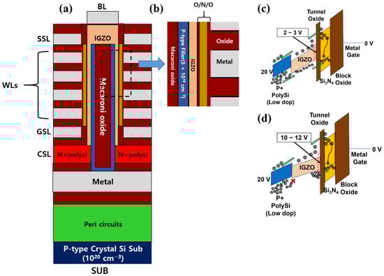
Figure 1.
Comparison of the proposed structures. Schematics of (a) are single strings of the IGZO-Filler (IF) structure in the COP device. (b) shows the details of the proposed structures. Finally, figures (c,d) describe the overall operation including the movement of the hole carrier during the erase operation in the IF structure.
Figures from (Figure 1c–d) illustrate the movement of electrons and holes by the erase operation (20 V) for each structure. The (Figure 1c) shows the band structure and the movement of each carrier at the time when 20 V, which is the erase operating voltage, is just applied (~1 μs) in the IF structure. The important point here is that due to the hole-related parameter characteristics of IGZO, unlike polysilicon channels, only a small amount of hole carriers are transferred to the channel. Next, as (Figure 1d) shows, when the voltage of the IGZO channel rises slightly (10–12 V) by a small number of hole carriers transmitted to the channel, the poor hole-related characteristics of the IGZO channel are overcome and the high voltage difference (~20 V) that the hole carriers could move disappears. After all, the hole carriers used for the erase operation in the IGZO channel are a small number of hole carriers that moved in the initial time when the erase voltage was applied.
In the IF structure, there is no need to forcibly transfer hole carriers in the crystal sub-area at the expense of the Peri circuit area as we proposed in previous studies [16]. Of course, this result is due to the low hole-related characteristics of IGZO, but in the case of using an IGZO channel, as shown in (Figure 1a), it is expected that the erase operation could be performed by adding only metal electrodes for voltage application to the upper region of the Peri circuit while keeping the lower structure the same as the existing 3D NAND structure. The fabrication process of this structure is basically the same as that mentioned in our previous paper [15]. However, as described above, the proposed structure does not require a passage to move hole carriers from the lowermost Crystal si sub-area, that is, an area created at the expense of the peri circuits area, and thus can fully preserve the Peri circuits area as shown in the figure. This structure is possible because, as will be described in the next chapter, the use of IGZO channels basically does not require many hole carriers.
3. Simulation Results and Discussion
3.1. Simulated Structures, Models, and Parameters
In this paper, we used a Synopsys Sentaurus TCAD devices simulator [16] to validate the proposed structure. First, the Structural Editor tool was used to design the proposed structure in Figure 2 below. In particular, the cylindrical command of the Sentaurus tool (Rotate 360 degrees) was able to form a virtual gate-all-around (GAA) structure based on half the 2D structure in device simulation. Using these features, we were able to simulate the entire vertical channel 3D NAND string and validate and analyze the overall behavior of the proposed devices. Next, the configuration of each contact point will be explained. First, the SUB contact at the bottom controls the voltage of the filler located inside the channel, and the CSL (Common-Source-Line) contact serves as the ground for the entire string. And the GSL (Ground-Select-Line) contact located on it controls the contact between CSL and the channel, and the 10 WL (Word Line) controls the operation of each memory cell. Finally, the source-select-line (SSL) bit line (BL) controls the contact between the channel, and the top BL acts as a drain.
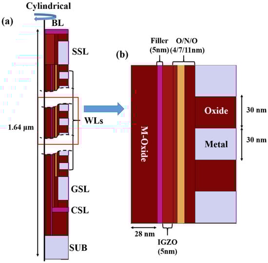
Figure 2.
Details of the simulated device. (a) Schematic of the 10 stacked memory cells, word lines WL0 to WL9, and select transistors, GSL, SSL, BL, and CSL. (b) Expanded view of the simulated structure with dimensions of the constituent parts.
Figure 2b shows an enlarged view of the dimensions of the elements used in the simulated device. The oxide, nitride, and block oxide layers of the tunnel were maintained at 4, 7, and 11 nm, respectively. In addition, as verified in previous studies, regardless of the thinness of the filler, and even if the thickness becomes too thin to deliver the hole carrier, it is confirmed that the erase operation can be performed up to 5 nm through the 2-step erase method [15]. Therefore, in this study, the thickness of the filler was set to 5 nm and the remaining area was filled with M-oxide. Thus, the total diameter of the simulation device is 100 nm. The word line gate length and the interval between successive word lines were fixed at 30 nm. While device simulation is in progress, the doping concentration dependence, high field saturation, and trap scattering mobility models were used. In addition, Shockley-Read-Hall [17], Auger [18], and Hurkx band-to-band recombination models [19] were also used to simulate the operation of the transistor in a V-NAND structure. In addition, the Poole–Frenkel model [20] and the nonlocal tunneling model [16] were used to model the electron and hole transport in silicon nitride.
Figure 3 shows the doping concentration of the formed structure and additional information on the SSL and GSL regions. First, in the case of the SSL region shown in (a), the length of the SSL gate is set to 100 nm, and this is also the case for the GSL in (b). This is for suppression of leakage current flowing to the BL and CSL, respectively, and enhancement of gate control capability. It is known that such a structure or a plurality of gates is used in the actual 3D NAND structure. Second, the doping concentration of the pillar was set to a lower concentration (5 × 1018 cm−3). This is in consideration of the difficulties in the process and the change of the threshold voltage due to the increase of the doping concentration. Lastly, as illustrated in Figure 2, unlike the SP structure of previous research [16], the lower SUB area is composed of pure metal electrodes.
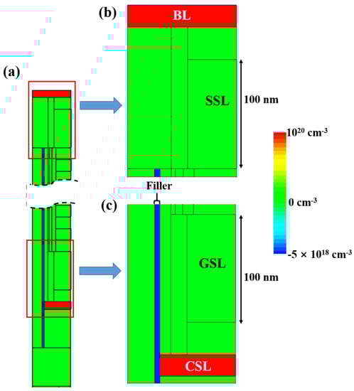
Figure 3.
Details of the doping concentration. Schematic of (a) the overall doping distribution, (b) the SSL region, and (c) the GSL and sub-region.
These changes can be expected to sacrifice the Peri circuit region in the previous SP structure and solve temperature problems that may occur during the process. Of course, this is also a possible structure because it is ironically difficult to deliver a large number of hole carriers in IGZO channels.
In addition, the parameters described in Table 1 were applied to polysilicon and silicon nitride for each material trap, and Table 2 shows the voltages applied to each operation. (Parameters other than the indicated trap parameters were basically applied from referenced papers [13,15,16]). Additionally, Figure 4 shows the result of simulating the actual measurement results of ref [21] (Figure 5a, VDS = 0.1 V) with simulated elements of the same scale by applying the parameters described above. As you can see, there are some differences, but we can see that the results are similar overall. These results show the reliability of the IGZO parameter used in this paper.

Table 1.
Trap parameters of each material.
Table 2.
The applied voltage for each operation.
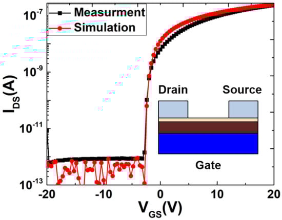
Figure 4.
IDS–VGS results between actual measurement and simulation in the TFT device.
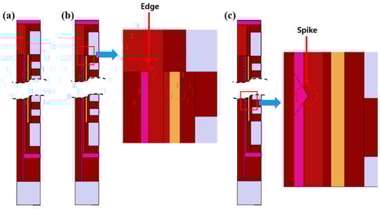
Figure 5.
Description of the three possible cases when the proposed IF structure is fabricated. (a) shows the most ideal process is assumed, and (b) shows the structure in which the filler structure edger is formed extremely sharply as a result of the top Chemical Mechanical Polishing (CMP) process being extremely well done. Finally, (c) shows the form in which spikes are formed on the contact surface between the filler and the IGZO channel due to various realistic problems occurring in the manufacturing process.
3.2. Simulation Results and Analysis When Applying IF Structure in COP Structure
First of all, we predicted that the following three situations will occur in the erase operation when real IGZO channels and filler structures are used in 3D NAND Flash memory through a more detailed simulation study. Figure 5 shows an explanation of the three possibilities mentioned above: First, as shown in (Figure 5a), if the filler and IGZO channels are not defective or problematic, the low hole characteristics of IGZO materials may not be overcome and the hole carriers may not be transferred to the IGZO channel. Of course, if a voltage much higher than the erase voltage currently in use (~30 V or more) is applied, the hole carriers may be transferred, but such an operation may be a great problem for both the channel and the filler.
Next, as shown in (Figure 5b), the uppermost end of the filler will be once the filler is formed and then planarized by the CMP process. However, in this process, if the CMP process goes very or extremely well, a very sharp edge will be formed as shown in the red circle in the figure. At these edges, even if the same voltage is applied, a much larger electric field will be formed, and thus the transfer of the hole carrier may be possible beyond the barrier due to the material characteristics of IGZO. Of course, there is a prerequisite that the quality of the CMP process must be very good in order to achieve this, but this assumption can also be considered because the current development speed of the CMP process is very fast. Finally, as shown in (Figure 5c), it is unlikely that the contact between the filler and the IGZO channel is absolutely flat and vertical, and rather there is a possibility that spikes may occur in the direction of the IGZO channel or in the opposite direction due to nonuniformity in the etching process or deposition process. These spikes may generate an electric field much stronger than other regions when an erase voltage is applied like the edge described above (Figure 5b), and through this, hole carriers may be transmitted to the IGZO channel. Therefore, this study will evaluate and analyze the influence of the erase operation on these three possibilities.
Figure 6 shows the results of the erase operation according to the interface state between the IGZO channel and the filler. First, when the interface state of the two materials is the most ideal, ironically, it shows the slowest erase operation speed. This result means that the hole carriers were not transferred to the IGZO channel through the filler at all, and the erase operation was purely an emission of electrons by the E-field. Next, where only one edge is present at the tip of the filler by the CMP process, it shows a faster operating speed than the previous result. Therefore, in this result, it can be confirmed that a small amount of hole carriers were supplied to the IGZO channel through a slight hole emission at the tip of the filler. Finally, the result of 1 edge + 6 spikes is the result of forming 6 spikes at arbitrary positions in the structure (Figure 5c) and performing the erase operation.
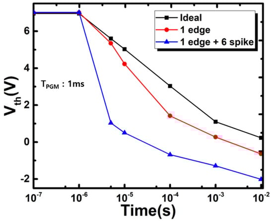
Figure 6.
Erase operation performance change according to filler state change (Vth: Threshold voltage).
Simulation results show the fastest erase operation speed as expected, and this result shows that hole carriers are discharged due to the same phenomenon in spikes as well as at the tip of the filler, and the erase operation is performed through it. Therefore, based on these results and the contents of Figure 1, the interface state between the filler and the IGZO channel would be ideal in the case where the erase speed in the 3D NAND flash memory with the IGZO channel and filler structure was the slowest, and in the case of the fastest, 1 edge +, it can be assumed that it will be in the state of 6 spikes. Of course, in the actual device, many more spikes may be formed than the simulation result, thereby releasing many hole carriers.
However, if a certain level of hole carrier is filled in the channel, the voltage of the channel will increase, and the E-field will be weakened due to the voltage difference between the filler and the IGZO channel so that the hole carriers cannot move. Therefore, increasing the spikes does not increase the erase rate indefinitely and it will eventually stagnate.
The results in Figure 7 can specifically explain the previously assumed content. First, in (Figure 7a–c), it can be observed that the interface where many spikes are generated delivers more hole carriers to the IGZO channel than the ideal interface. However, this does not mean that all hole carriers are filled in the channel like the Polysilicon channel, and as shown in the cross-sectional result (Figure 7c), the density at which hole carriers can actually transmit voltage is filled to only 2 nm near 40 nm, which is the interface with the tunnel oxide. Therefore, as shown in the voltage distribution from (Figure 7d–f), the voltage drop is of course very severe in the ideal interface state, but even in the presence of spikes, the voltage rise increased by only 6.3 V. Therefore, it can be seen that the channel voltage at this time, specifically the voltage at the tunnel oxide contact surface, is 13.7 V, and the difference from the filler voltage of 18 V is only about 4.3 V. In other words, when such a small voltage difference is formed, it can be confirmed that the hole carriers can no longer overcome the low hole characteristics of IGZO and cannot be transmitted to the channel.
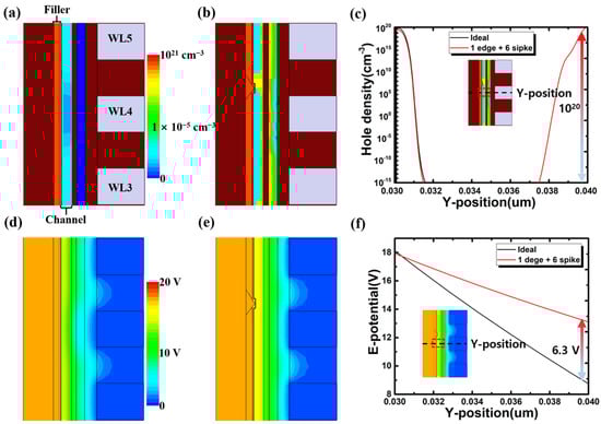
Figure 7.
Comparison of Hole Density and Electric potential (E-potential) Change among the erase operation characteristics according to the state of the interface in the proposed IF structure. (a,b) show the hole carrier density when the erase operation proceeds to 10 μs. (c) shows cross-sectional results on the channel. Next, (d,e) show the voltage distribution at the same erase operation time. And (f) shows cross-sectional results.
These results indicate, as we explained earlier, that it is meaningless to form many spikes to increase the erase operation efficiency, and also why it is not necessary to supply the hole carrier from the crystal sub to the filler at the expense of the peri circuit area. Simply put, hole carriers that can be transferred to the IGZO channel or necessary hole carriers can only fill a thickness of 1–2 nm at the interface between the tunnel oxide and the channel, and these filled hole carriers increase the voltage of the channel but at the same time reduce the voltage difference between the filler and the channel. This reduced voltage difference eventually makes it impossible to transfer the hole carrier to the channel, and the increase in the hole carrier density of the channel becomes stagnant. Thus, the interface state of the filler and IGZO channels in the proposed structure should not be an unconditional ideal state, but it also does not require numerous spikes for hole carrier transmission. Currently, it is difficult to control the process for forming these spikes due to process limitations, but if process technology develops thereafter, it will be possible to precisely control the proper formation of the spike and secure maximum erasing efficiency.
Through the previous results, we confirmed that even if realistic process conditions are applied, the proposed structure overcomes the adverse hole-related characteristics of IGZO in the 3D NAND flash memory structure to which the IGZO channel is applied and enables a fast erase operation. Next, we will examine the points that may be of concern with respect to the application of the IGZO channel and the filler structure. The first thing to be considered before applying the proposed IF structure is whether the leakage current increases. This is because, although considered and verified in the IP structure of previous studies, when the pillar and the channel are in direct contact, the pillar itself becomes a pass for the leakage current and there is a possibility of increasing the leakage current.
First, as illustrated in Figure 8a, the leakage current in the reading operation is about 10−15 A, which is well maintained at low leakage current characteristics. This is one of the advantages of IGZO materials, compared to the existing 3D NAND Flash structure using the PolySilicon channel that is about 10−13 A [15]. In particular, a leakage current to the SUB contact is 10−20 A, which is actually 0, and if the filler thickness is sufficiently thin, it is expected that the leakage current would not occur in this direction regardless of the filler doping concentration.
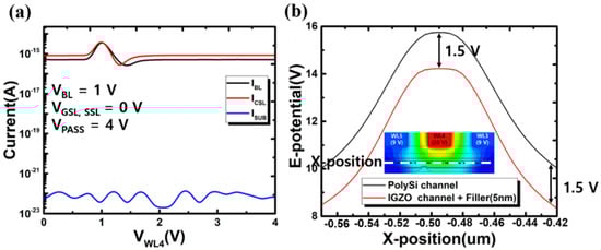
Figure 8.
Verification results of problems that may arise when the IF structure performs operations other than erase operation. (a) Analysis results of the correlation between leakage current passing through the filler in the read operation and another leakage current of BL, CSL and SUB. (b) It shows that the channel potential is increased through self-boosting in certain cell strings that are in the program inhibited Mode.
Next, the channel potential change shown in (b) represents a channel-boosting performance change to inhibit programming behavior on an unselected string when the program operation is performed on the selected string in the 3D NAND structure [22]. This “self-boosting” technique is an operation of increasing a channel voltage within a string sharing the same BL among strings to be programmed to suppress programming behavior [22].
Assuming the string to which the corresponding action is applied, it can be observed that when the filler thickness is 5 nm in the proposed IGZO channel + IF structure, the channel potential is 1.5 V lower than the general 3D NAND structure. This phenomenon is thought to be affected by the channel potential directly connected to the column because the sub-contact connected to the column is in the ground state. On top of that, since the IGZO channel itself has a weak N-type characteristic and an average carrier density of about 1017 cm−3, it is considered that an additional voltage drop occurs. However, even in the IGZO channel + Filler structure, the channel voltage could be raised to 14.2 V through the self-boosting technique, and at this voltage, the difference from the program operating voltage of 20 V is only 5.8 V, so it seems that the original role of preventing program operation can be sufficiently performed.
Finally, Table 3 shows the results of comparing the typical 3D NAND with the strengths and weaknesses of the proposed structure. First, in the case of program operation speed, it is expected that all three structures to be compared will be almost the same. This is because the voltage of the channel in the program operation is fixed in the GND state, so the factors that affect the program operation performance are the type and quality of the ONO layer and WL metal, and basically, all three structures are the same structure and process. Second, in the case of erase operation speed, it can be seen that the proposed IF structure is absolutely excellent. In particular, these advantages will be able to stably solve the problem of erasure speed degradation that may occur when gate stacks of 300 to 500 or more are used due to future technological advances. This is because the filler that supplies hole carriers in the proposed IF structure is basically doped with P-type, so it is hardly affected by the increase in height. Third, the leakage current, which was feared to be a problem of directly coupling the filler to the channel, confirmed a very small leakage current of 10−15 A by properly controlling the doping concentration of the filler in addition to the inherent low leakage current characteristics of the IGZO material. This can be expected to dramatically reduce standby power consumption, one of the most important considerations, especially for mobile devices. Forth, it has been confirmed that the self-boosting performance is about 1.5 V lower than that of a typical 3D NAND flash structure. However, this lowered channel boosting voltage is only a 5.8 V difference from the program voltage, so it is expected that the original role of preventing the program from operating will be performed without any problems.
Table 3.
Various comparison results between previously announced structures and the proposed structure.
Finally, if you compare the three structures in terms of the manufacturing process, the SP structure proposed in the previous study first needs to deliver hole carriers to the filler from the crystal sub-area at the bottom, so two types of filler structures are required for this. Therefore, there was a problem that the Peri circuit area was sacrificed and the process cost was greatly increased compared to the existing 3D NAND structure. However, in the case of the new IF structure proposed this time, the erase operation is possible with only a small amount of hole carriers by reversely using the material properties of IGZO, so the cost of increasing the process can be minimized because only one filler adjacent to the channel is sufficient.
4. Conclusions
In this paper, we proposed an improved IF structure that can be used for 3D NAND structures with recent COP structures based on IP structures that could supply holes in channels in crystal bulk regions such as TCAT published in previous studies and validated and analyzed them through device simulations. In particular, despite IGZOs very poor hole-related properties, the proposed structure shows that hole carriers present in the filler can be delivered to the channel through spikes that can occur in a realistic process, and it has been confirmed that hole carriers can be delivered to the channel without sacrificing the area of the peri circuit. At this time, the hole erase operation speed of the IF structure is about 100 μs, and the erase operation is performed only by the filler adjacent to the channel. In addition, the leakage current characteristics of the IGZO channel can be maintained without being affected by the filler, and the channel voltage is reduced by 1.5 V compared to the existing structure, but the difference from the program voltage is only 5.8 V, so the original purpose of preventing the program operation can be fully achieved. In conclusion, the proposed IF structure is judged to be the optimal solution for using IGZO material as a channel for 3D NAND Flash memory. In particular, we believe that this structure is the best approach because it can overcome the poor hole carrier properties of IGZO and deliver hole carriers essential for the erase operation of CTF memory. Therefore, if the structure proposed in this paper is applied to the 3D NAND Flash structure, IGZO channels that were not available in the 3D NAND Flash structure can be used, which will solve problems (leak current, temperature instability, etc.) in the current 3D NAND Flash structure at once.
Author Contributions
Methodology, paper writing, investigation, conceptualization, and validation, S.C.; review, M.K.; funding acquisition, supervision, and editing, Y.-H.S. All authors have read and agreed to the published version of the manuscript.
Funding
This work was supported by the National Research Foundation of Korea (NRF) grant funded by the Korean government (MSIT) (grant No. 2021R1A2C2093415) and was supported by Samsung Electronics through the Future Non-Volatile Memory Cluster Academia Collaboration Program. Also, this work was supported by the Technology Innovation Program (20016366) funded By the Ministry of Trade, Industry and Energy (MOTIE, Republic of Korea).
Data Availability Statement
Not applicable.
Conflicts of Interest
The authors declare no conflict of interest.
References
- Tanaka, H.; Kido, M.; Yahashi, K.; Oomura, M.; Katsumata, R.; Kito, M.; Fukuzumi, Y.; Sato, M.; Nagata, Y.; Matsuoka, Y.; et al. Bit Cost Scalable Technology with Punch and Plug Process for Ultra High Density Flash Memory. In Proceedings of the Symposium on VLSI Technology, Kyoto, Japan, 12–14 June 2007; pp. 14–15. [Google Scholar] [CrossRef]
- Jang, J.; Kim, H.S.; Cho, W.; Cho, H.; Kim, J.; Shim, S.L.; Jang, Y.; Jeong, J.H.; Son, B.K.; Kim, D.W.; et al. Vertical Cell Array usingTCAT (Terabit Cell Array Transistor) Technology for UltraHigh Density NAND Flash Memory. In Proceedings of the Symposium on VLSI Technology, Kyoto, Japan, 15–17 June 2009; pp. 192–193. [Google Scholar]
- Choi, E.S.; Park, S.K. Device Considerations for High Density and Highly Reliable 3D NAND Flash Cell in Near Future. In Proceedings of the IEDM Electron Devices Meeting, San Francisco, CA, USA, 10–13 December 2012; pp. 211–214. [Google Scholar] [CrossRef]
- International Roadmap for Devices and Systems™. 2022. Available online: https://irds.ieee.org/editions/2022 (accessed on 3 May 2023).
- Wang, B.; Gao, B.; Wu, H.; Qian, H. A drain leakage phenomenon in poly silicon channel 3D NAND flash caused by conductive paths along grain boundaries. Microelectron. Eng. 2018, 192, 66–69. [Google Scholar] [CrossRef]
- Tang, B.; Luque, M.T.; Zhang, W.D.; Bosch, G.V.; Degraeve, R.; Zhang, J.F.; Houdt, J.V. Statistical characterization of vertical poly-Si channel using charge pumping technique for 3D flash memory optimization. Microelectron. Eng. 2013, 109, 39–42. [Google Scholar] [CrossRef]
- Nomura, K.; Ohta, H.; Takagi, A.; Kamiya, T.; Hirano, M.; Hosono, H. Room-temperature fabrication of transparent flexible thin-film transistors using amorphous oxide semiconductors. Nature 2004, 432, 488–492. [Google Scholar] [CrossRef] [PubMed]
- Kamiya, T.; Hosono, H. Material characteristics and applications of transparent amorphous oxide semiconductors. NPG Asia Mater. 2010, 2, 15–22. [Google Scholar] [CrossRef]
- Kimizuka, N.; Yamazaki, S. Physics and Technology of Crystalline Oxide Semiconductor CAAC-IGZO: Fundamentals; Wiley: New York, NY, USA, 2016; p. 232. [Google Scholar]
- Honda, R.; Suzuki, A.; Matsuda, S.; Saito, S.; Shima, Y.; Koezuka, J.; Yamazaki, S. Electrical Characteristics of Dual-Gate CAAC-IGZO FET with Self-Aligned Top Gate. SID Symp. Dig. Tech. Pap. 2016, 47, 1132–1135. [Google Scholar] [CrossRef]
- Wu, S.H.; Jia, X.; Li, X.; Shuai, C.C.; Lin, H.C.; Lu, M.C.; Wu, T.H.; Liu, M.Y.; Wu, J.Y.; Matsubayashi, D.; et al. Performance Boost of Crystalline In-Ga-Zn-O Material and Transistor with Extremely Low Leakage for IoT Normally-off CPU Application. In Proceedings of the on VLSI Circuits, Kyoto, Japan, 5–8 June 2017; pp. 166–167. [Google Scholar] [CrossRef]
- Kim, J.; Kang, S.; Jang, Y.; Lee, Y.E.; Kim, K.; Kim, W.; Lee, W.; Hwang, C. Investigating the Reasons for the Difficult Erase Operation of a Charge-Trap Flash Memory Device with Amorphous Oxide Semiconductor Thin-Film Channel Layers. Phys. Status Solidi 2020, 15, 2000549. [Google Scholar] [CrossRef]
- Choi, S.; Kim, B.; Jeong, J.K.; Song, Y.H. A Novel Structure for Improving Erase Performance of Vertical Channel NAND Flash with an Indium-Gallium-Zinc-Oxide Channel. IEEE Trans. Electron Devices 2019, 66, 4739–4744. [Google Scholar] [CrossRef]
- Lim, J.; Chung, S.; Ko, D.-H.; Sung, S.-K.; Noh, K.; Ahn, S.; Song, J. Development of 7th generation 3D VNAND Flash Product with COP structure for Growing Demand in Storage Market. In Proceedings of the 2020 International Conference on Electronics, Information, and Communication (ICEIC), Jeju, Republic of Korea, 6–9 February 2022. [Google Scholar] [CrossRef]
- Choi, S.; Kim, B.; Jeong, J.K.; Song, Y.H. Innovative structure to improve erase speed in 3D NAND flash memory with Cell-On-Peri (COP) applied. IEEE Trans. Electron Devices 2022, 69, 4883–4888. [Google Scholar] [CrossRef]
- Synopsys, Inc. Sentaurus Device User Guide; Version J-2014.9; Synopsys, Inc.: Mountain View, CA, USA, 2014. [Google Scholar]
- Fossum, J.G.; Mertens, R.P.; Lee, D.S.; Nijs, J.F. Carrier Recombination and Lifetime in Highly Doped Silicon. Solid-State Electron. 1983, 26, 569–576. [Google Scholar] [CrossRef]
- Huldt, L.; Nilsson, N.G.; Svantesson, K.G. The temperature dependence of bandto-band Auger recombination in silicon. Appl. Phys. Lett. 1979, 35, 776–777. [Google Scholar] [CrossRef]
- Hurkx, G.A.M.; Klaassen, D.B.M.; Knuvers, M.P.G. A New Recombination Model for Device Simulation Including Tunneling. IEEE Trans. Electron. Devices 1992, 39, 331–338. [Google Scholar] [CrossRef]
- Colalongo, L.; Valdinoci, M.; Baccarani, G.; Migliorato, P.; Tallarida, G.; Reita, C. Numerical Analysis of Poly-TFTs under off Conditions. Solid-State Electron. 1997, 41, 627–633. [Google Scholar] [CrossRef]
- Kwon, J.Y.; Jeong, J.K. Recent progress in high performance and reliable n-type transition metal oxide-based thin film transistors. Semicond. Sci. Technol. 2015, 30, 024002–024017. [Google Scholar] [CrossRef]
- Sim, J.M.; Kang, M.; Song, Y.H.K. A Novel Program Operation Scheme with Negative Bias in 3-D NAND Flash Memory. IEEE Trans. Electron. Devices 2021, 68, 6112–6117. [Google Scholar] [CrossRef]


Disclaimer/Publisher’s Note: The statements, opinions and data contained in all publications are solely those of the individual author(s) and contributor(s) and not of MDPI and/or the editor(s). MDPI and/or the editor(s) disclaim responsibility for any injury to people or property resulting from any ideas, methods, instructions or products referred to in the content. |
© 2023 by the authors. Licensee MDPI, Basel, Switzerland. This article is an open access article distributed under the terms and conditions of the Creative Commons Attribution (CC BY) license (https://creativecommons.org/licenses/by/4.0/).