Abstract
A Ka-band low-profile and low-loss tile-type four-beam network based on high-density interconnection printed circuit board (PCB) technology is proposed, which integrates a power supply network, serial peripheral interface (SPI) control network, and four-beam radio frequency (RF) feeding network. In order to realize the fast optimal design, an integrated multi-beam network topology and fast optimization methods are established. The proposed feed networks can be integrated with antenna array structures directly, which not only realizes low-profile, light, and miniaturized design but also achieves efficient heat dissipation and low-loss interconnection. The designed multi-beam network has an amplitude balance better than ±0.5 dB and a phase balance better than ±6° in the Ka-band with a 4 GHz working bandwidth. A prototype was fabricated and measured, and good performance was observed.
1. Introduction
With the rapid growth of mobile broadband multimedia services and the urgent need to build high-throughput satellites and low-orbit mobile Internet satellites that need higher data transmission capacity and transmission rates, multi-beam phased array antennas with features of wide bandwidth, high gain, small size, light weight, and wide beam coverage are preferred [1,2,3].
As a key component of multi-beam phased array antennas, multi-beam antennas operating at higher frequency and greater beam numbers are a very hot research topic in the antenna and microwave community. Due to the high-density integration of power supply, SPI control, and RF multi-beam feed networks in the very limited space, crosstalk between digital and radio frequency signals is difficult to suppress. In addition, it is very time-consuming to design and optimize the network with traditional 3D full-wave electromagnetic field simulation software. Phased array antennas based on printed circuit board (PCB) multi-layer board technology are introduced in [4,5,6,7,8,9,10], while it only works in one beam and the network can be realized using one layer of strip-line. At the same time, the specifications and types of buried blind holes involved are relatively small with a relatively simple stacked structure. Multi-beam networks based on low-temperature co-fired ceramics (LTCC) technology are introduced in [11,12]. However, it is a brick structure, and the traditional subminiature push-on (SMP) connector is used to feed the antenna. Therefore, it is bulky and expensive. In [13,14], there is an introduction to the feed network based on PCB multi-layer boards. However, the maximum beam number is two, and there are no details on the fast optimization design method.
A Ka-band low-profile tile-type four-beam network based on the HDI PCB (high-density interconnect printed circuit board) process, which integrates power supply, SPI control, and an RF four-beam feeding network, is proposed. By establishing a multi-beam integrated network topology and a rapid optimization method, the optimal design of the network is realized. The proposed feeding networks can be integrated with antenna array structures directly, which not only realizes low-profile, light, and miniaturized design but also achieves efficient heat dissipation and low-loss interconnection.
2. Proposed Design of the Multi-Beam Network
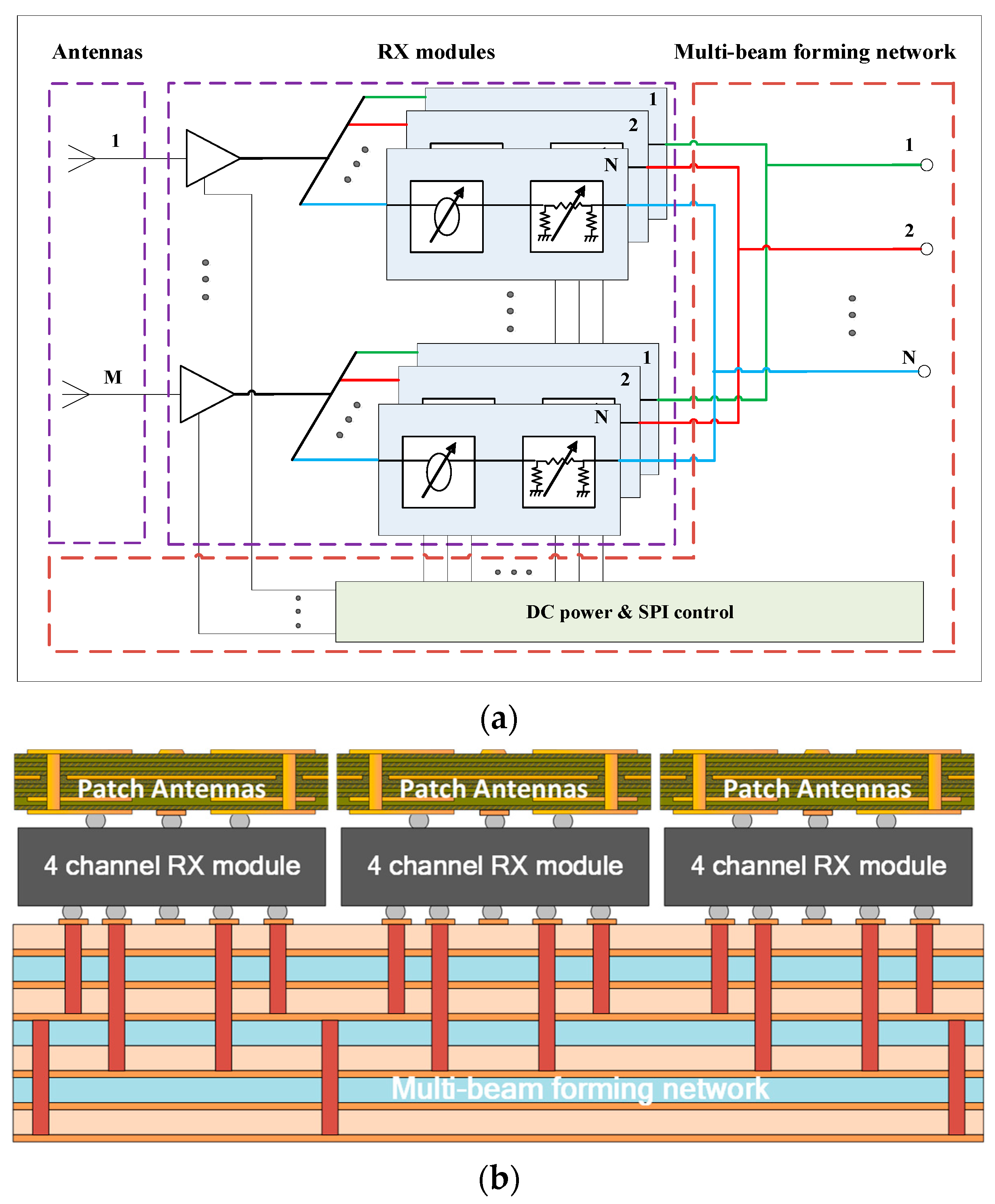
2.1. Architecture of the Multi-Beam Phased Array Antenna
A schematic diagram of a typical receiving multi-beam network is shown in Figure 1a. It consists of M (M denotes the number of antenna elements) input and N (N denotes the number of beams) output ports, so the number of power distribution networks is M × N, which is very difficult in limited space, especially in millimeter waves.
Figure 1.
Architecture of the multi-beam phased array antenna: (a) schematic diagram of the typical multi-beam receiving phased array antenna and (b) the proposed architecture.
An architecture with features of low loss, low profile, and low cost for a multi-beam phased array antenna is proposed in this paper, as shown in Figure 1b. The entire antenna consists of three layers. The first layer is the passive antenna array. Each sub-array antenna consists of four antenna elements arranged in 2 × 2 and realized by a PCB board. The second layer is the multi-beam module, which is packaged in ceramics and mainly integrates a low-noise amplifier, a beam power division network, and a multi-function chip (MFC). The input ports and output ports are located on the front and back side of the component, respectively. The upper layer is interconnected with the antenna array while the down layer is interconnected with the multi-beam network. Both of them are interconnected with BGA solder balls to reduce loss. The third layer is a multi-beam network, which is implemented by a high-precision microwave multi-layer PCB board, which integrates a DC power supply, SPI control, and an RF multi-beam network.
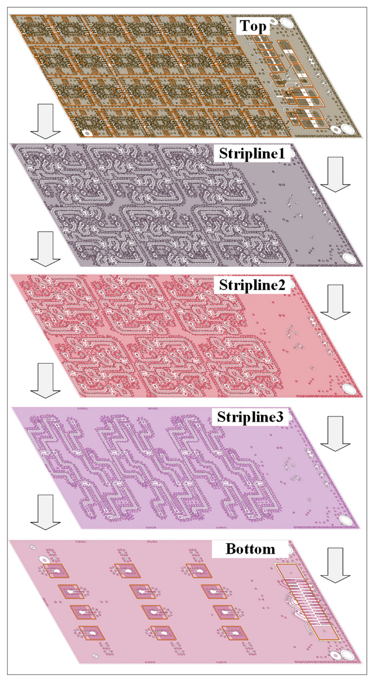
2.2. Multi-Beam Network Design Based on Multilayer PCB Stack-Up
Since there are multiple sets of power divider networks and many types of interconnection signals, multi-layer strip-lines and different types of internal buried blind visas are required for implementation. They are difficult to fabricate due to the limited number of multilayer PCB board laminations and the back drilling process.
A four-beam network operated at Ka-band is proposed in this paper. The laminated structure of the multi-layer PCB board used for the proposed network is 19 layers, as shown in Figure 2. The thickness of the core board is 5 mil and 10 mil, while the thickness of the prepreg layer is 5 mil. The RF transmission lines are ball grid array (BGA) pads, a grounded co-planar waveguide, and a strip-line, which are respectively distributed on the 1st, 7th, 11th, 15th, and 19th layers. The power supply control signal lines are distributed on the second, third, and fourth layers. Signal isolation and shielding are realized through the ground layer between the RF and low-frequency signal lines.
Figure 2.
Proposed multi-beam network layer distribution on PCB technology.
There are five specifications of buried blind holes. They connect the BGA pads of the receive components to the first and second strip-line layers, the first strip-line layer to the third strip-line layer, the second strip-line layer to the third strip-line layer, and the third strip-line layer to the bottom small subminiature push-on (SSMP) connectors. In addition, the fifth layer is set as a copper-based metal layer, which improves the heat capacity of the network and facilitates better heat dissipation.
The RF layout of the proposed design is shown in Figure 3. The networks of beam 1 and beam 3 are distributed in the first strip-line layer (strip-line 1), and the networks of beam 2 and beam 4 are distributed in the second strip-line layer (strip-line 2). The 1:2 power dividers of these four beams are distributed in the third strip-line layer (strip-line 3). Input ports are placed on the top layer while the output ports are placed on the bottom layer.
Figure 3.
Layered diagram of the radio frequency layout for the four-beam network.
Due to the high density of the circuit layout, three-dimensional vertical interconnection in the Z-direction space of the multi-layer board is employed to satisfy the space requirement and reduce the heavy signal crosstalk. Shielding ground vias are set on both sides of the strip-lines of each layer and between the lines. The via spacing is generally less than one-twentieth of the wavelength under the premise of meeting the processing capability of the process. In order to ensure a better shielding effect, a double row of staggered vias is used. Considering that the working frequency is the Ka-band, which is sensitive to the process parameters, it is necessary to accurately model according to the process realization capability and conduct tolerance analysis on the detailed parameters. For example, the length of the via stub formed via back drilling, the minimum distance between the transmission line and the shielding ground, the size of the via plates in different layers, and the size of the anti-pad of each layer, etc.
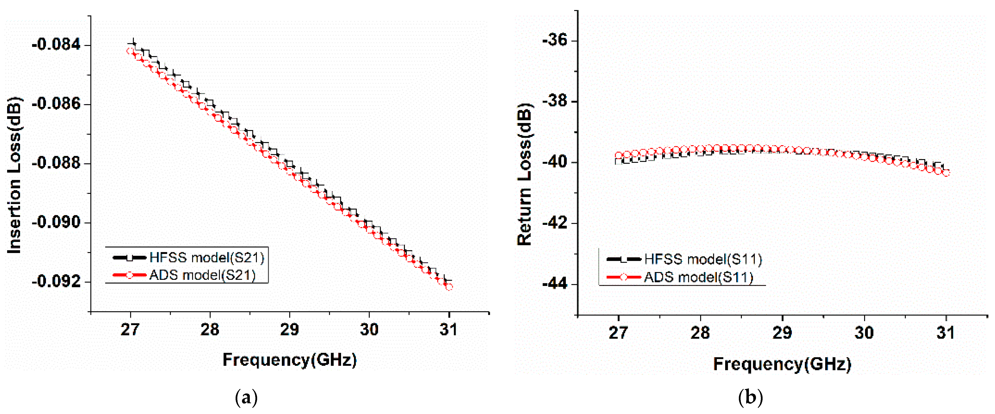
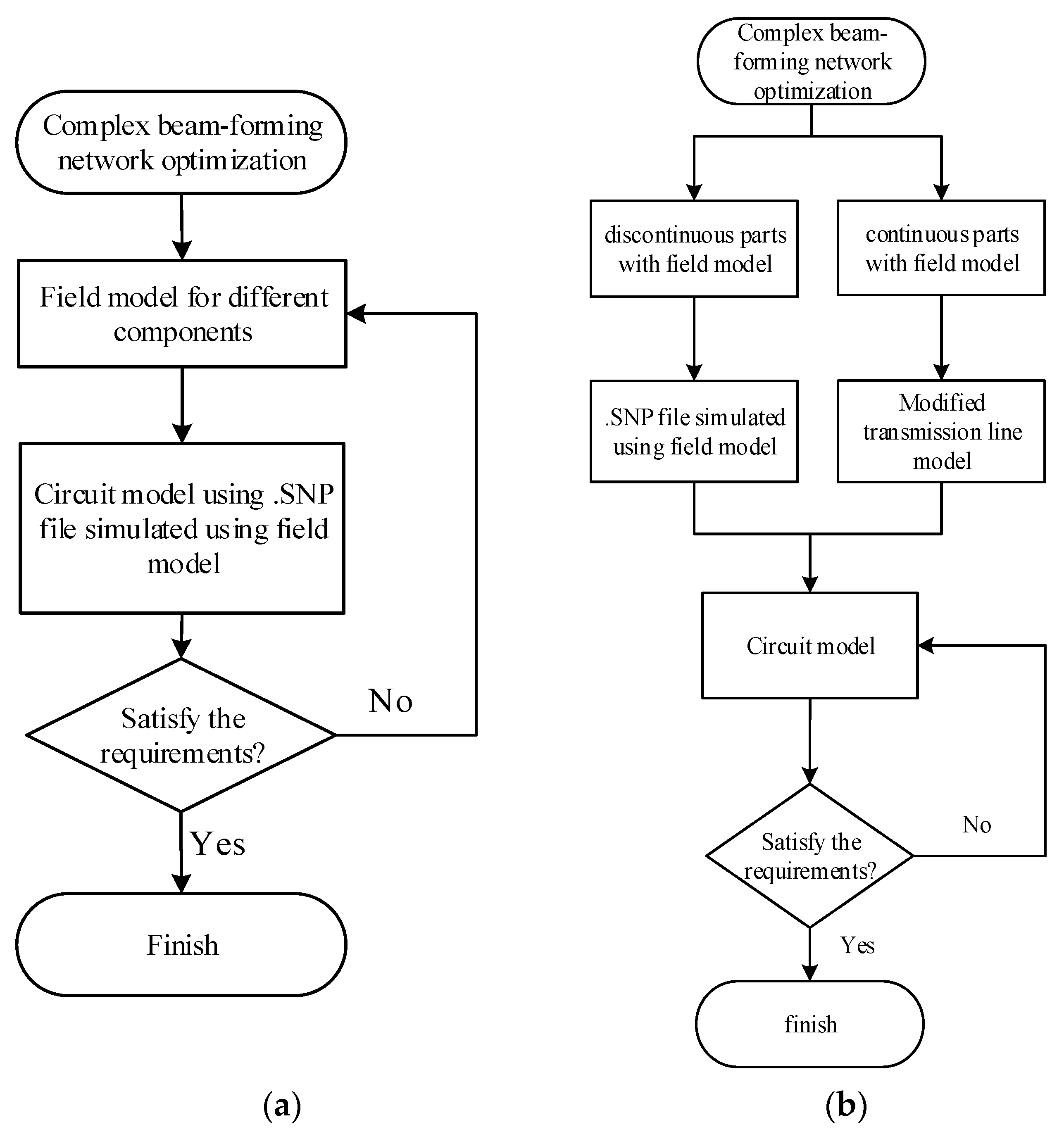
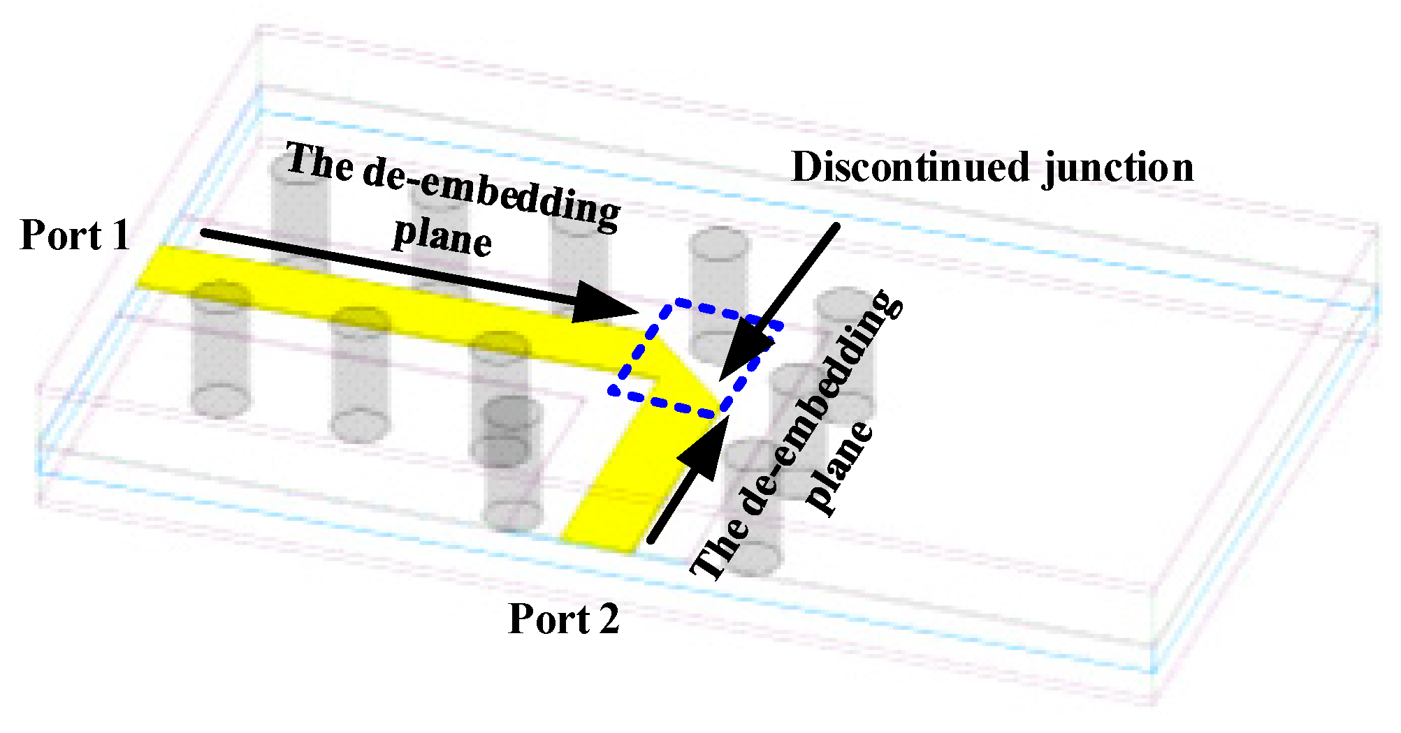
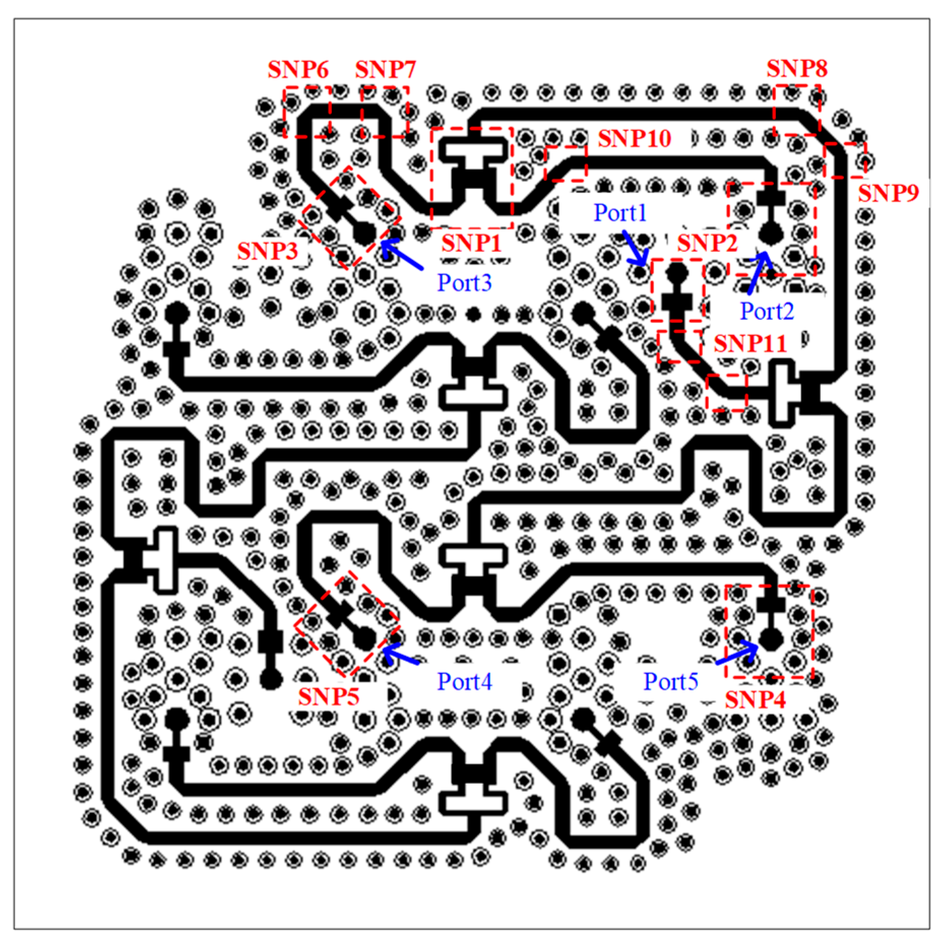
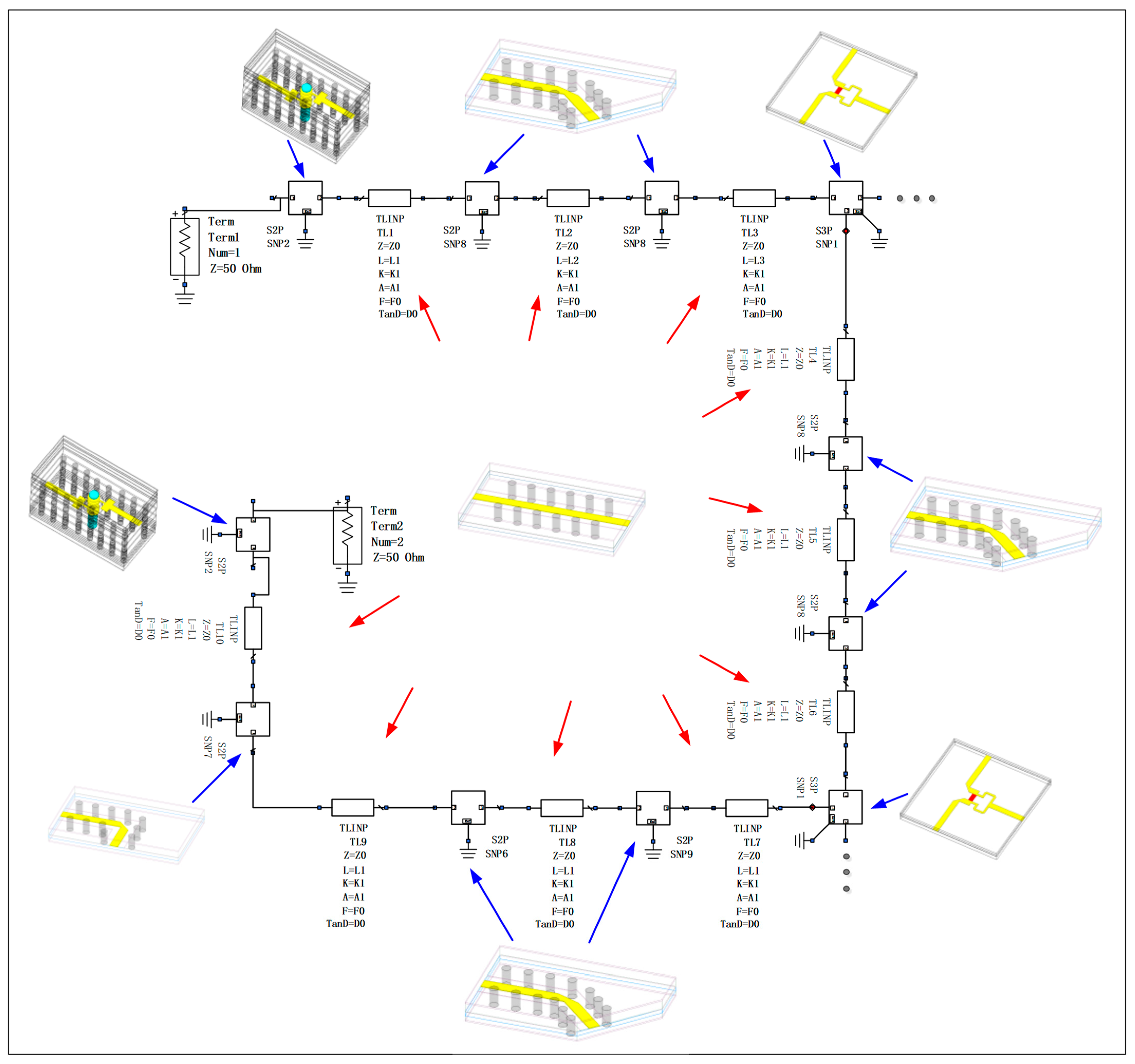
2.3. Multi-Beam Network Simulation Optimization
Due to the complex circuit distribution, it is difficult and almost impossible to simulate the proposed multi-beam network using the traditional 3D full-wave electromagnetic wave method, while if the traditional transmission line model is used, it is not accurate because the effects of via holes and the non-uniformity of the substrate (realized by the multilayer structure with prepreg) are not considered.
The transmission line model in ADS software is shown in Figure 4; its performance is characterized by parameters Z, L, K, A, and TanD. Z is the characteristic impedance, L is the length, K is the equivalent dielectric constant, A is the transmission loss per unit length, and TanD is the loss tangent. All of the parameters are obtained using the theoretical formula for the traditional method, while they are obtained with the curve fitting method in our paper. With the modified parameters, good agreement between the circuit model (ADS software) and field model (HFSS software) is observed, as shown in Figure 5. Therefore, the modified transmission line model proposed in this paper addresses the issues between accuracy and efficiency.
Figure 4.
Circuit model of the shielding strip-line.
Figure 5.
Performance comparison of the circuit model with the field model with the modified transmission line model: (a) insertion loss and (b) return loss.
The flow chart of our proposed method and existing design methods is shown in Figure 6. For the traditional field-circuit collaborative optimization method, it is time-consuming and requires large computer memory because the parameters are tuned in the field model, while for the proposed method, it has the advantages of fast and accuracy because the parameters are tuned in the circuit model. In order to establish an equivalent circuit model, the proposed multi-beam network circuit is divided into two parts. For the discontinuous parts of the circuit, such as the strip-line to strip-line transitions of different layers, transformation junctions with right-angle cut corners, etc. Equivalent circuit models are very complex (thousands of capacitors and inductors), so full wave simulation is employed to obtain the S parameters (.SNP data file) of the discontinuous parts. For the continuous part of the circuit, such as the grounded coplanar waveguide transmission line, the shielded cavity strip-line, etc., the parameters can be obtained with the above-modified transmission line theory.
Figure 6.
Flow chart of the traditional field-circuit collaborative optimization method and the proposed method: (a) traditional field-circuit collaborative optimization method and (b) the proposed method.
In addition, de-embedding technology is used for the three-dimensional model, as shown in Figure 7. For the three-dimensional field model of the discontinuous part of the transformation junction, a certain distance is de-embedded when setting the reference plane, so that the port and the discontinuity have a certain distance so that the parasitic high-order modes can be sufficiently attenuated and disappear. The same method is also applicable to other discontinuous parts in the multi-beam network circuit, such as the matching transformation junction of high- and low-impedance lines, etc.
Figure 7.
Schematic diagram of the reference surface setting of the right-angle chamfer model.
Based on the proposed method, the equivalent circuit of a 1:4 power divider shown in Figure 8 can be established in Advanced Design System (ADS) software. The equivalent circuit model is shown in Figure 9 and the simulated results are shown in Figure 10. Good agreement is observed between the proposed method and the full wave simulation method.
Figure 8.
The 1:4 power divider layout.
Figure 9.
The 1:4 power divider equivalent circuit model.
Figure 10.
Results comparison of the 1:4 power divider using the proposed method and the full wave solver: (a) insertion loss and (b) return loss.
Table 1 shows the comparison of two optimization methods for the multi-beam network model (with shielding vias) that is shown in Figure 3. The field-circuit collaborative optimization method proposed in this paper has great advantages in terms of computer memory requirements and simulation time.
Table 1.
Comparison of the two simulation optimization methods.
Table 2 shows the performance comparison of the proposed network with other recently published works. The proposed network has the highest beam numbers, better gain imbalance, and phase imbalance while maintaining the advantages of being lightweight and low cost.
Table 2.
Performances comparison of the proposed network with other recently published works.
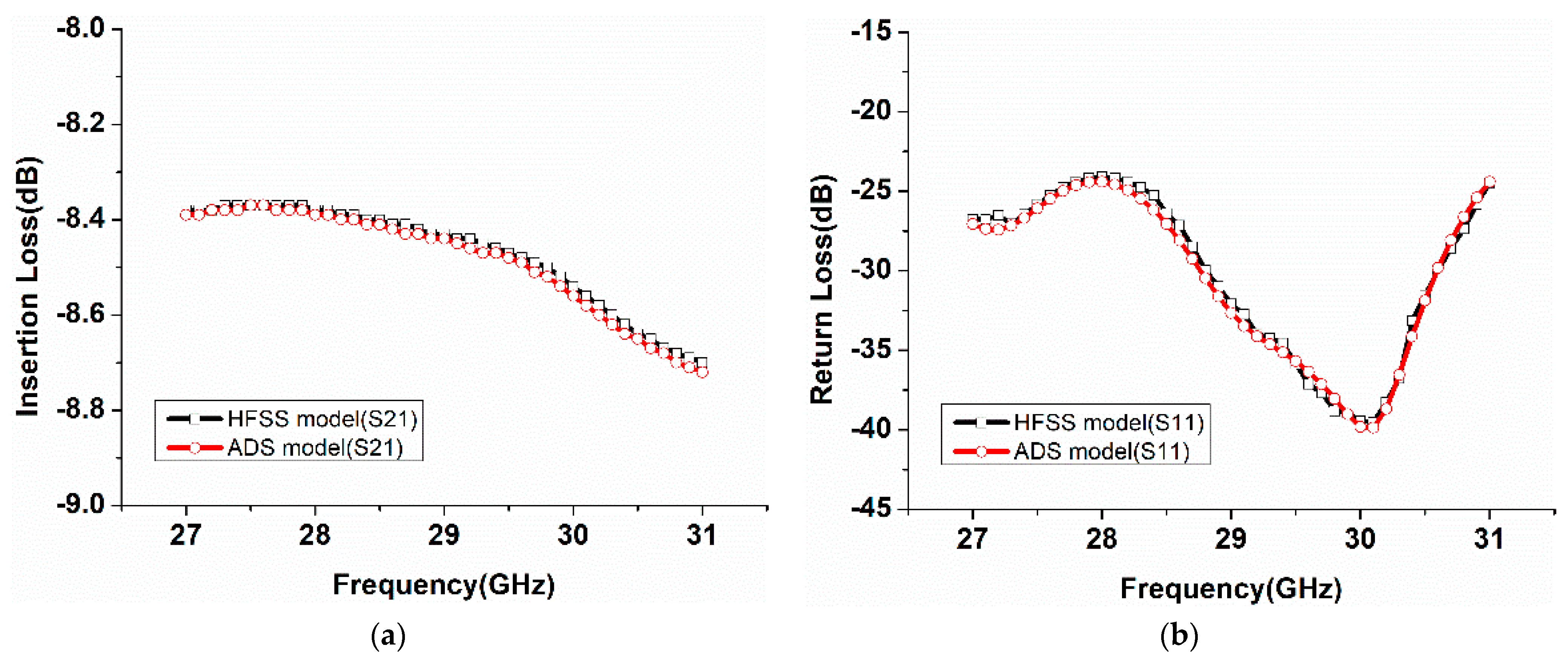
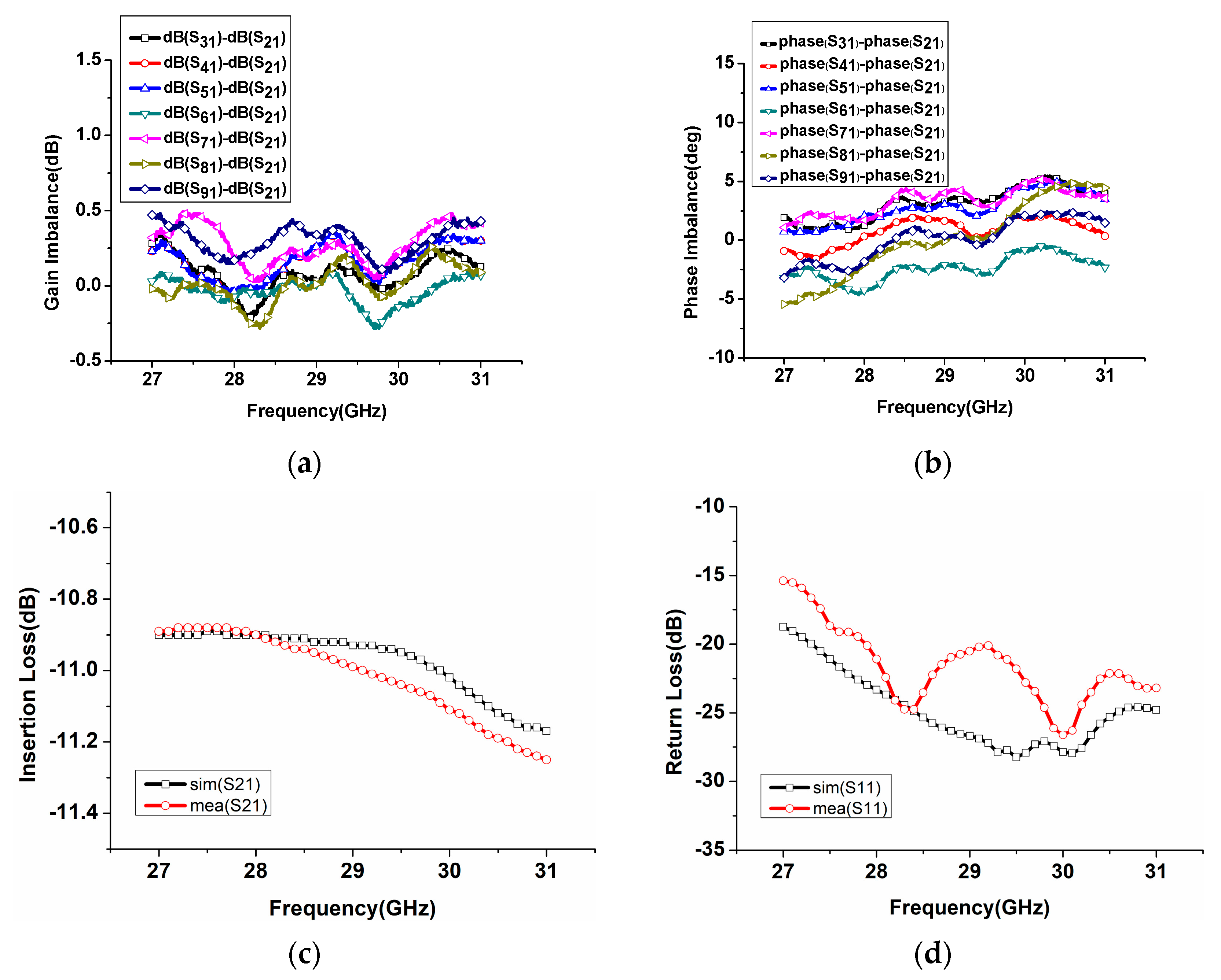
3. Fabricated Prototype and Measured Results
A TSM-DS3 dielectric substrate and FR28-0040 prepreg were selected to design and fabricate the proposed four-beam network. The dielectric constant and loss tangent of TSM-DS3 are 3.0 and 0.0025, respectively, while the dielectric constant and loss tangent of FR28-0040 are 2.8 and 0.0020, respectively. As shown in Figure 11, the size of the board is 84 mm × 42 mm × 4 mm. The input ports of the networks are placed on the front side, which is used to connect the BGA flip chip beam formers component, while the output ports of the networks are placed on the back side, which are used to connect the antenna arrays.
Figure 11.
Photograph of the four-beam network: (a) front side and (b) back side.
Agilent N5224A PNA which covers 10 MHz~43.5 GHz was used to measure the proposed network. The working band is set to 27~31 GHz, and the SOLT (short, open, through, and load) calibration method was employed. The measured result is shown in Figure 12. As illustrated in Figure 8, the amplitude balance is in the range of +/−0.5 dB, and the phase balance is in the range of ±6°. Good agreement is observed between the simulated and measured return loss and insertion loss, which verifies the proposed design.
Figure 12.
The measured results of the four-beam network: (a) amplitude imbalance; (b) phase imbalance; (c) insertion loss; and (d) return loss.
4. Conclusions
The architecture topology of the Ka-band multi-beam network which is the core component of the multi-beam phased array antenna is presented in this paper. The field-circuit collaborative method is employed to optimize the proposed design. The fabricated four-beam network is tested. The measured results show that the amplitude balance is better than ±0.5 dB, while the phase balance is better than ±6° within the whole 4 GHz working bandwidth. The proposed method can be extended to the design of other multi-beam networks, which has important theoretical guidance and can promote the development of low-profile tile-type multi-beam phased array antennas for wireless communication systems.
Author Contributions
Conceptualization, X.Y.Z., J.Y., Y.L. and B.Z.; methodology, X.Y.Z., M.L. and X.R.Q.; validation, X.R.Q.; writing—original draft preparation, X.Y.Z.; writing—review and editing, X.Y.Z., R.X.L. and Y.L.; supervision, J.Y., Y.L. and B.Z. All authors have read and agreed to the published version of the manuscript.
Funding
This research was supported by the National Key Research and Development Program of China under No. 2019YFB1803200.
Data Availability Statement
Not applicable.
Conflicts of Interest
The authors declare no conflict of interest.
References
- Lambard, T.; Lafond, O.; Himdi, M.; Jeuland, H.; Bolioli, S.; Le Coq, L. Ka-band phased array antenna for high-data-rate SATCOM. IEEE Antennas Wirel. Propag. Lett. 2012, 11, 256–259. [Google Scholar] [CrossRef]
- Portillo, I.D.; Cameron, B.G.; Crawley, F. A technical comparison of three low earth orbit satellite constellation systems to provide global broadband. Acta Astronaut. 2019, 159, 123–135. [Google Scholar] [CrossRef]
- Lee, K.M.; Edie, J.; Krueger, R.; Weber, J.; Brott, T.; Craig, W. A low profile X-band active phased array for submarine satellite communications. In Proceedings of the IEEE International Conference on Phased Array Systems and Technology, Dana Point, CA, USA, 21–25 May 2000; pp. 231–234. [Google Scholar]
- You, D.; Takahashi, Y.; Takeda, S.; Moritani, M.; Hagiwara, H.; Koike, S.; Lee, H.; Wang, Y.; Li, Z.; Pang, J.; et al. A Ka-Band 16-Element Deployable Active Phased Array Transmitter for Satellite Communication. In Proceedings of the 2021 IEEE/MTT -S International Microwave Symposium (IMS), Virtual Event, 20–25 June 2021; pp. 799–802. [Google Scholar]
- Abdel-Wahab, W.M.; Al-Saedi, H.; Alian, E.H.M.; Raeis-Zadeh, M.; Ehsandar, A.; Palizban, A.; Ghafarian, N.; Chen, G.; Gharaee, H.; Nezhad-Ahmadi, M.R.; et al. A Modular Architecture for Wide Scan Angle Phased Array Antenna for K/Ka Mobile SATCOM. In Proceedings of the 2019 IEEE MTT-S International Microwave Symposium (IMS), Boston, MA, USA, 2–7 June 2019; pp. 1076–1079. [Google Scholar]
- Navarro, J.A. Heterogeneously- Integrated Phased-Array Antennas for Line—of—Sight (LOS) Communications and Sensor Applications. In Proceedings of the 2018 IEEE/MTT-S International Microwave Symposium (IMS), Philadelphia, PA, USA, 10–15 June 2018; pp. 776–778. [Google Scholar]
- Navarro, J. Affordable, Multi-Function Flight-Worthy Airborne Phased-Array Sensor. In Proceedings of the 2020 IEEE/MTT -S International Microwave Symposium (IMS), Los Angeles, CA, USA, 4 August–30 September 2020; pp. 829–832. [Google Scholar]
- Aljuhani, A.H.; Kanar, T.; Zihir, S.; Rebeiz, G.M. A scalable dual-polarized 256-element ku-band phased-array SATCOM receiver with ±70° beam scanning. In Proceedings of the IEEE MTT-S International Microwave Symposium Digest, Philadelphia, PA, USA, 10–15 June 2018; pp. 1203–1206. [Google Scholar]
- Low, K.K.W.; Nafe, A.; Zihir, S.; Kanar, T.; Rebeiz, G.M. A scalable circularly-polarized 256-element ka-band phased-array SATCOM trans-mitter with ±60° beam scanning and 34. 5 dBW EIRP. In Proceedings of the EEE MTT-S International Microwave Symposium Digest, Boston, MA, USA, 2–6 June 2019; pp. 1064–1067. [Google Scholar]
- Low, K.K.W.; Zihir, S.; Kanar, T.; Rebeiz, G.M. A Scalable Switchable Dual-Polarized 256-Element Ka-Band SATCOM Transmit Phased-Array with Embedded RF Driver and ±70° Beam Scanning. In Proceedings of the 2020 IEEE/MTT-S International Microwave Symposium (IMS), virtual event, 12–14 October 2020; pp. 821–824. [Google Scholar]
- Kassner, J.; Kulke, R.; Uhlig, P.; Rittweger, M.; Waldow, P. Highly Integrated Power Distribution Networks on Multilayer LTCC for Ka-band Multiple-Beam Phased Array Antennas. In Proceedings of the IEEE MTT-S CDROM, Seattle, WA, USA, 2–7 June 2002; pp. 51–54. [Google Scholar]
- Butz, J.; Spinnler, M.; Christ, J.; Mahr, U. Highly integrated RF-modules for Ka-band multiple-beam active phased array antennas. In Proceedings of the IEEE MTT-S CDROM, Seattle, WA, USA, 2–7 June 2002; pp. 61–64. [Google Scholar]
- Nafe, A.; Sayginer, M.; Kibaroglu, K.; Rebeiz, G.M. 2 × 64 Dual-Polarized Dual-Beam Single-Aperture 28 GHz Phased Array with High Cross-Polarization Rejection for 5G Polarization MIMO. In Proceedings of the 2019 IEEE MTT-S International Microwave Symposium (IMS), Boston, MA, USA, 2–6 June 2019; pp. 484–487. [Google Scholar]
- Nafe, A.; Sayginer, M.; Kibaroglu, K.; Rebeiz, G.M. 2 × 64-element dual-polarized dual-beam single-aperture 28-GHz phased array with 2 × 30 Gb/s links for 5G polarization MIMO. IEEE Trans. Microw. Theory Technol. 2020, 68, 3872–3884. [Google Scholar] [CrossRef]
Disclaimer/Publisher’s Note: The statements, opinions and data contained in all publications are solely those of the individual author(s) and contributor(s) and not of MDPI and/or the editor(s). MDPI and/or the editor(s) disclaim responsibility for any injury to people or property resulting from any ideas, methods, instructions or products referred to in the content. |
© 2023 by the authors. Licensee MDPI, Basel, Switzerland. This article is an open access article distributed under the terms and conditions of the Creative Commons Attribution (CC BY) license (https://creativecommons.org/licenses/by/4.0/).