1. Introduction
Although silicon is still the dominant semiconductor material in microelectronics, its physical limitations are more and more visible, keeping the parameters of manufactured devices from meeting the current expectations of the market. Therefore, new semiconductor materials are sought-after to solve the problem. Particularly, the investigations are focused on wide bandgap (WBG) semiconductors, whose physical parameters exceed the silicon ones. Generally, they are characterized by larger band gaps, higher melting temperatures, better heat conductivity, a larger electron saturation velocity and greater critical electric field strength. In WBG materials, one can distinguish between the group of technologically-mature semiconductors (SiC and GaN) and the group of promising semiconductors currently under research (Ga
2O
3, III-Ns) [
1,
2].
The above parameters allow for the manufacturing of devices characterized by unattainable or very difficult-to-attain ratings when manufactured with silicon or other semiconductors. The large critical electric field strength enables the attainment of high-voltage p-n junctions with a breakdown voltage larger than 10 kV [
3,
4,
5,
6]. The large band gap makes possible the manufacturing of low-noise devices or devices working at high temperatures exceeding even 700 °C [
6,
7,
8], as well as optoelectronics devices for “blue optoelectronics” [
9,
10]. The large saturation electron velocity makes them an excellent candidate for high-frequency devices with possible maximal frequencies reaching THz [
11,
12]. Good thermal conductivity is very crucial from a reliability point of view (thermal stresses) and for thermal-management problems [
7].
This paper deals with the problems of silicon carbide technology. The basic obstacle in the practical use of silicon carbide in electronics consists of different, very often extreme, demands concerning the technology processes in comparison to the processes of silicon technology. This causes the technology processes and characterization procedures that are well known in silicon technology to often be inappropriate in the case of silicon carbide. Research on silicon-carbide-based semiconductor devices has been carried out in a number of scientific centers for many years [
13,
14,
15]. As a result, rapid progress in the quality of fabricated SiC single crystals, as well as semiconductor devices built in that material, can be observed. Moreover, a demonstration of practically all types of SiC discrete semiconductor devices has already been presented. However, this situation does not transfer into the wide availability of these devices on the market. The commercial offer of silicon carbide devices is currently limited mainly to Schottky diodes, MESFETs, MOSFETs, JFETs and some optoelectronic devices. The main difficulties standing in the way of the practical use of silicon carbide in modern electronics are different, and often extreme, requirements for technological processes as compared to silicon. As a result, the technological processes and characterization methods developed for silicon turn out to be not fully suitable or not adaptable to new needs. For instance, those processes must be carried out at much higher temperatures due to the higher melting point of silicon carbide (~2100 °C) as compared to silicon (1410 °C), since the initiation of any crystal relaxation processes and dopant diffusion requires significantly higher temperatures than in the case of silicon. This had a significant influence on the adaptation of doping methods from silicon technology to SiC ones. Due to their similarities, the adaptation of epitaxy processes was rather easy and, at present, is dominant in SiC technology [
16]. The adaptation of ion implantation has also been, to some extent, completed. It required the modification of the ion gun and the high-temperature annealing processes to reduce radiation damage and to position the impurity atoms at electrically-active lattice sites [
17]. The thermal diffusion method, however, being the basic one in Si technology, is still under development in the case of SiC technology [
18,
19].
Critically high temperatures are required during post-implantation annealing and doping via the thermal diffusion of dopants in SiC. In the case of doping, temperatures exceeding 1800 °C are indispensable to ensure the effectiveness of this process. At such temperatures, silicon sublimation occurs and leads to gradual degradation of SiC crystal surface layers, making this process technologically challenging. Due to the significantly higher temperature, it requires different technological, controlling and measuring equipment than in the case of diffusion processes in silicon. On the other hand, it also requires the maintenance of process atmosphere conditions that would act against the negative effects of sublimation. For those reasons, although thermal diffusion is considered the cheapest and most welcome technology, particularly in power device manufacturing, there were not many attempts to adapt the diffusion technology to the needs of SiC [
18,
19,
20], and the published results so far are not satisfactory. The lack of such a technology was an impetus to undertake research on the development of an effective technology for doping in SiC substrates for the research group from the Department of Semiconductor and Optoelectronic Devices at Lodz University of Technology [
21,
22], where an experimental unit quipped with a graphite reactor built on the basis of a modified Degussa VLS10/18 furnace has been used.
The starting point for the undertaken research was the assumption that the occurrence of uncontrolled processes during the annealing of silicon carbide can be significantly reduced by maintaining the processed wafers in a state of equilibrium between sublimation and epitaxial growth, as a result of the creation of an atmosphere containing a gaseous form of SiC. The implementation of this solution requires maintaining a homogeneous temperature in the reactor during annealing and placing an additional source of carbon and silicon vapors in the vicinity of the annealed SiC substrate. In order to create such process conditions, a closed graphite cassette was introduced into the reactor chamber, where the processed silicon carbide structure was placed in the vicinity of the SiC powder acting as the source of volatile Si, C, Si
2C and SiC
2 gases, saturating the atmosphere inside the cassette and blocking the degradation of the surface of the SiC substrate being heated. The conducted experiments produced promising effects in terms of the blocking of the sublimation process in the annealed SiC substrates, and proved that it is possible to carry out effective experiments of thermal diffusion of selected impurities in silicon carbide [
23].
The transfer of the processed silicon carbide structure into the closed graphite cassette made direct in situ pyrometric measurement of its temperature through the inspection window impossible. Such a measurement was only possible for the upper surface of the graphite cassette that covered up access to the processed structure. Since the monitoring of the SiC sample temperature is critically important for the proper diffusion process flow, it was decided to introduce an indirect method involving the use of the CAD approach to estimate the sample temperature on the basis of a pyrometric measurement of the temperature on the surface of the cassette. For this purpose, a numerical model of phenomena occurring in the Degussa furnace reactor was developed. Such a model was created on the basis of the commercial ANSYS 11.0 package [
24], allowing simulation of thermal fields under given heat-dissipation conditions in the modeled area and in the presence of gaseous and liquid media participating in heat exchange and transport.
It is worth noting that although CAD tools are commonly used in microelectronics technology to support the design of devices [
25], their manufacturing processes [
26,
27,
28,
29] or the investigation of semiconductor features [
30], their use as an element of measuring set-up that controls the technology process is presented here, probably for the first time. This paper presents the construction details of the Degussa furnace reactor with an additional cassette for SiC processing, which was the starting point for the creation of a numerical model of the phenomena occurring in the reactor during high-temperature processes, as well as the subsequent stages of CAD model development and verification of taken assumptions. The effectiveness of the worked-out model is presented as well.
2. Materials and Methods
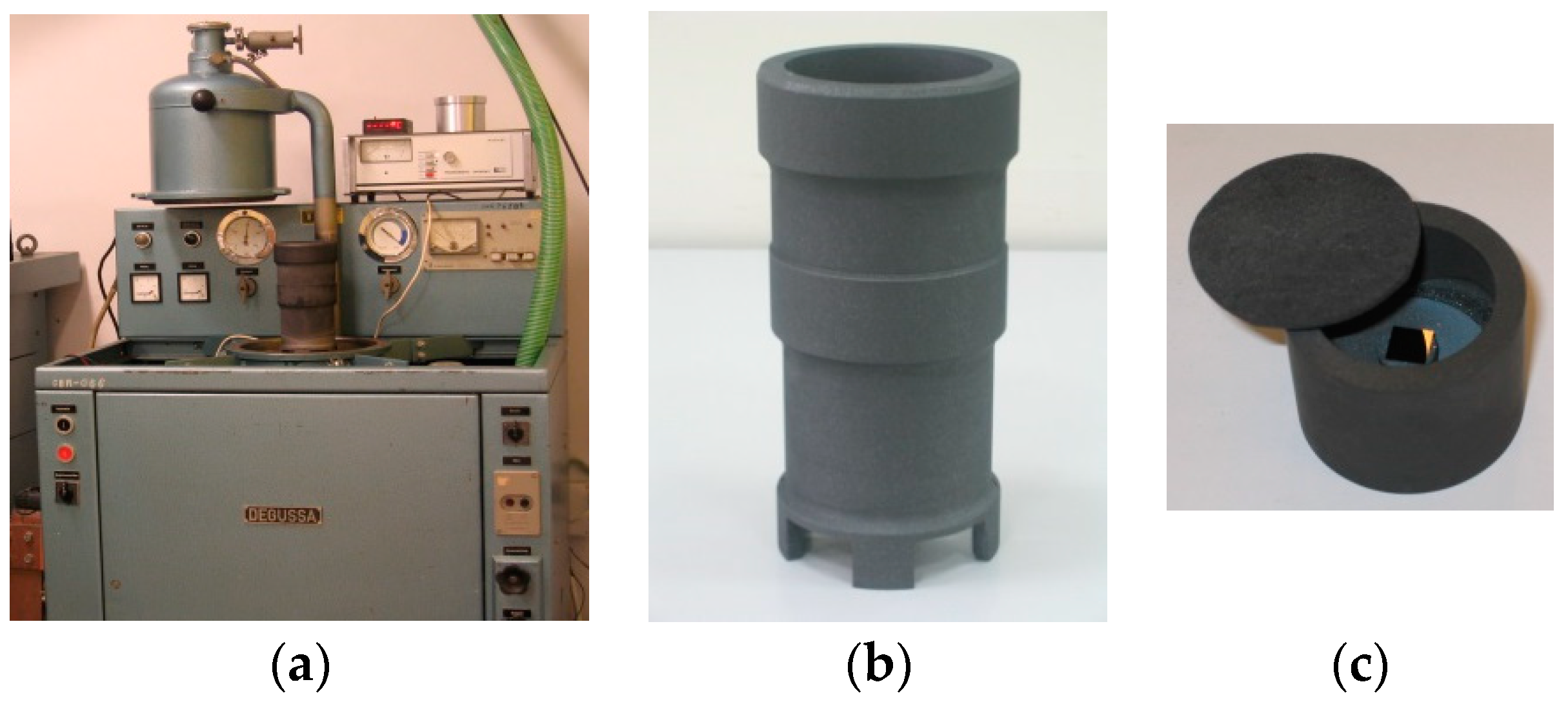
In general, there are serious problems with the availability of processing equipment dedicated to SiC technology, in particular those enabling realization of annealing processes at temperatures up to 2000 °C. Therefore, it was decided to adapt for these purposes the VSL10/18 industrial furnace from Degussa Wolfgang, shown in
Figure 1a. The furnace was originally intended for the sintering, annealing, brazing and melting processes at both reduced and elevated pressures relative to atmospheric pressure. It is equipped with heating elements made of molybdenum, chromium-nickel, graphite, tantalum or tungsten, which allow it to obtain different maximal temperatures. Using a graphite reactor (
Figure 1b), which was chosen for the processing of SiC structures, it is possible to reach temperatures up to 2200 °C, which are sufficient for the high-temperature silicon carbide technology. Its basic operating parameters are also suitable for research in this area. It is equipped with a 20 kW power supply system, a vacuum system with a low (rotary) and high (diffusion) vacuum pump, a liquid cooling system and the ~20 L reactor chamber. Additionally, it is possible to measure the temperature by means of a thermocouple, or by optical methods through an inspection window made of quartz glass in the furnace. The pressure in the reactor chamber can be measured by means of pressure sensors with standardized vacuum joints.
The adaptation of the VLS10/18 furnace to conduct high-temperature processes in silicon carbide technology required a number of adjustments. They included the introduction of a non-invasive pyrometric temperature measurement system for the reactor’s interior through an inspection window, a pressure measurement system, as well as a gas supply with flow controls for both inert shielding gases and working gases. The most important element of these adjustments, however, was to create conditions preventing the occurrence of uncontrolled processes during the annealing of silicon carbide by maintaining the processed samples in a state of equilibrium between sublimation and epitaxial growth. This was achieved by introducing an additional closed graphite cassette, shown in
Figure 1c, into the reaction chamber. In this cassette, the processed silicon carbide structure was placed in the vicinity of the SiC powder, which acted as a source of volatile Si, C, Si
2C and SiC
2 gases saturating the atmosphere inside the cassette and blocked the degradation of the surface of the heated SiC substrate.
Obtaining the conditions enabling the reduction in uncontrolled processes during the annealing of silicon carbide requires maintaining the processed SiC samples in a state of equilibrium between sublimation and epitaxial growth, and in particular, ensuring a uniform temperature in the graphite cassette placed in the reactor. Unfortunately, the ability to control the temperature changes in the reactor is limited to the pyrometric measurement of the temperature Tp at the bottom of the reactor in the absence of the cassette and the temperature Td of the cover of the cassette when it is placed inside the reactor.
During the adjustments to the reactor, measurements of these temperatures were made using a Raytek MR1SC pyrometer installed above the inspection window of the steel chamber of the reactor, as shown in
Figure 2. They were made under the conditions expected during the foreseen high-temperature SiC processes, i.e., at a pressure of 1 Pa in the reactor and with 9 kW power dissipated in the heater, which correspond to the temperature of about 1700 °C in the working area of the furnace at steady state. The results of those measurements are presented in
Table 1. They show that the difference in these temperatures, when carrying out the annealing process, is too large to assume that the temperature T
d equals the temperature of the processed structure positioned inside the cassette; another method of control is needed. For this purpose, it was decided to use the CAD approach to estimate this temperature. This required the development of a steady-state numerical model for the SiC structure annealing process in the cassette placed in the reactor, accurate enough to enable both the verification of the temperature homogeneity in the cassette and the determination of the SiC structure temperature based on the measurement of the T
d temperature. The research leading to this model is presented in the following chapters.
3. Basic Model of Reactor
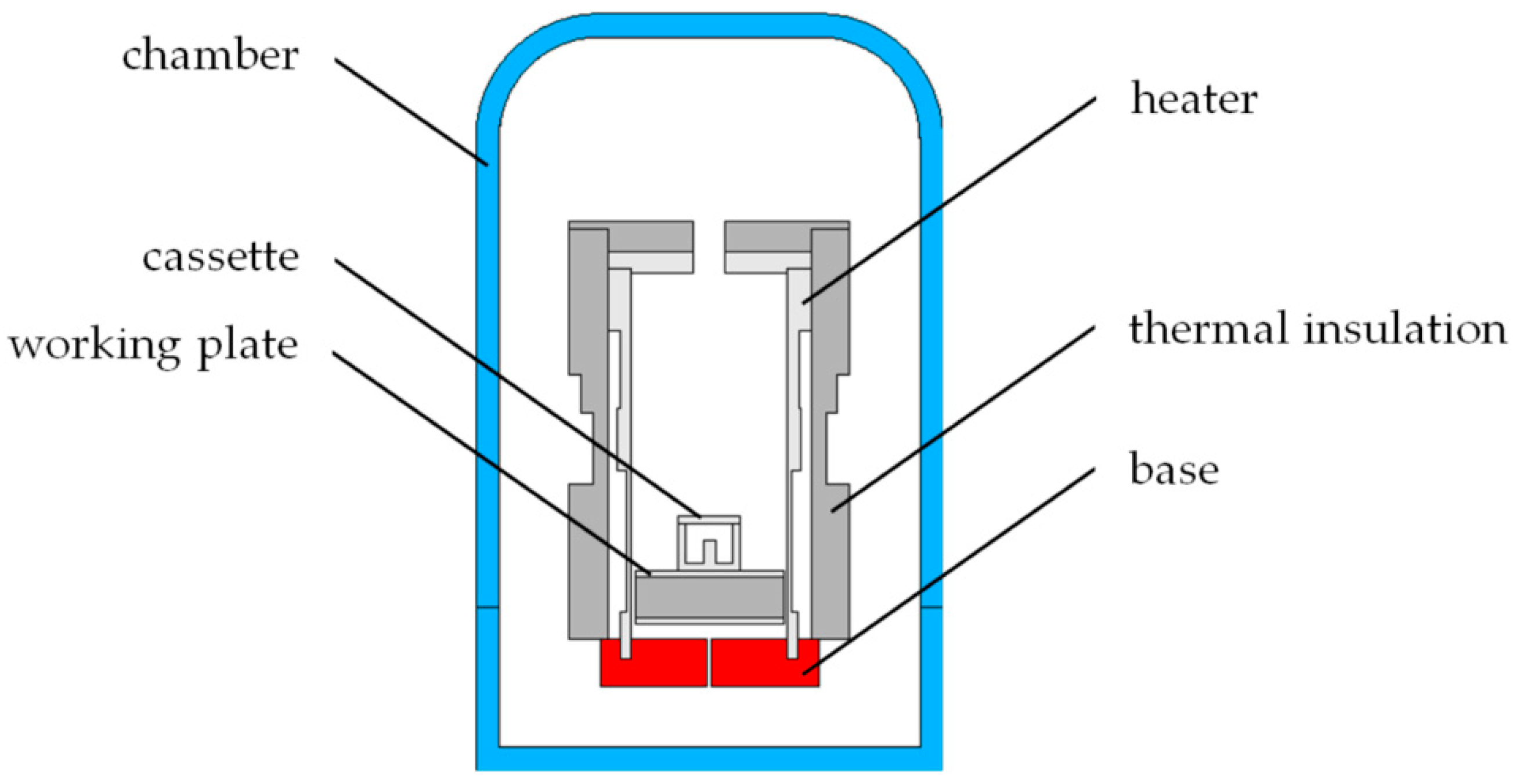
The first step of the numerical research was to create a numerical model of the reactor using the ANSYS package employing the finite element method to numerically solve the heat transport equations. This model, defined as the K1 model, covers the space limited to the furnace’s chamber, as shown in
Figure 3. It includes a steel cover, a copper base (acting also as an electrode delivering current to the heater), a graphite heater with thermal insulation made of carbon fiber and a graphite plate constituting the working plate in the reactor.
In the model, it is assumed that:
The working chamber has axial symmetry, which allows the phenomena to be considered two-dimensional in cylindrical coordinates;
The steel chamber is a cylinder topped with an upper part shaped like a flattened hemisphere;
The graphite heater has a cylinder shape with a constant internal radius of 50 mm and a variable external radius;
In the model, the graphite heater is formed by five rings with different outer radii, which results in different heat-dissipation densities at the same constant current;
Table 2 summarizes the outer radii of these rings and the heat dissipation density occurring at a supplying power of 9 kW, as recommended in
Section 2;
The developed model is a precise geometric reflection of the actual structure of the reactor; the only difference concerns the omitted mounting elements, such as screws and inlet and outlet connections to the chamber used for argon flow;
The existence of a liquid cooling system in the copper base and in the steel chamber was taken into account by introducing the boundary condition of the constant temperature of external surfaces, corresponding to the typical temperature of the coolant (by default T = 30 °C was assumed);
The furnace operates at a significantly reduced pressure in the working chamber; therefore, it has been assumed that there is no heat transport in it as a result of convection, and the only effective heat flow paths are diffusion heat flow in the area of solids and heat exchange by radiation;
It was assumed that copper surfaces do not participate in heat exchange by radiation in the reactor chamber due to their location;
The emissivity factor for all internal surfaces of the steel chamber was assumed to be 0.20, while the emissivity factor for graphite surfaces was 0.80 [
31];
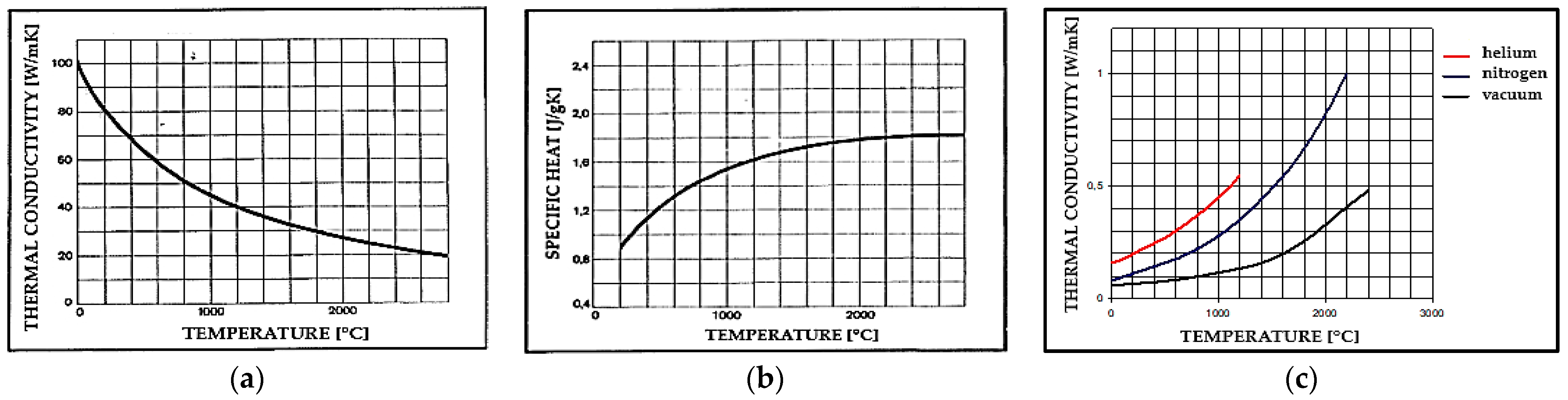
The physical parameters of the materials used for the individual elements adopted in the model are summarized in
Table 3; some of them have been assumed to be temperature-dependent and are described by the non-linear functions presented in
Figure 4.
For the above assumptions, the ANSYS software generated a discretization mesh, presented in
Figure 5, for simulations using the finite element method. Its characteristic feature is that it only consists of elements with diffusive heat flow. The space between these elements is treated as a vacuum in which only radiative heat flow can occur, and therefore no mesh nodes are present here.
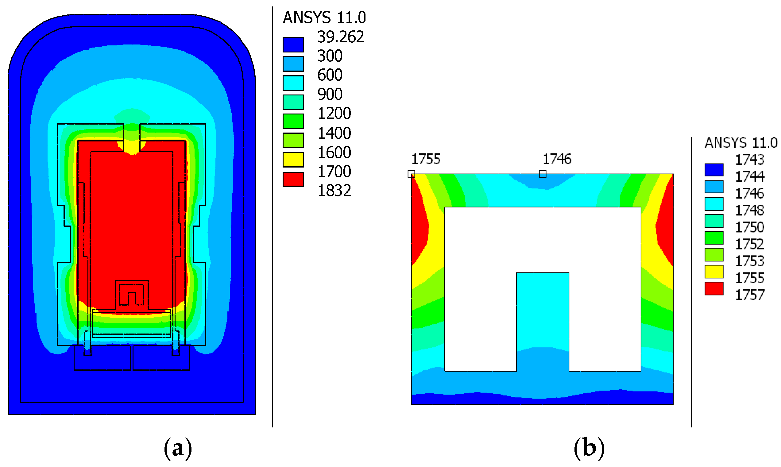
The temperature distribution inside the Degussa furnace reactor and in the graphite cassette obtained for the input power 9 kW are shown in
Figure 6. The temperature gradient between the upper and bottom sides of the cassette equals 14 °C, as shown in
Figure 6b, while between the graphite bar and the bottom of the cassette, it does not exceed 3 °C, which is a desirable situation during the high-temperature SiC doping process. However, the temperature of the upper surface of the cover equals 1770 °C, which is a value 38 °C higher than the values measured by the pyrometric method in real processing at the same input power. This difference corresponds to 2.2% of the measured value, which from a metrological point of view is an unacceptably large estimation error. In order to obtain a smaller discrepancy between the experimental data and the obtained result of the simulation estimation, it was decided to modify the numerical model of the reactor.
4. Advanced Model of Reactor
In order to simplify the simulations, the K1 model assumed that there was no gas in the reactor chamber. In real conditions, high-temperature SiC annealing processes are usually carried out in an atmosphere of an inert gas with a pressure typically ranging from 1 to 1000 Pa. Therefore, in the modified K2 model, the presence of working gas has been taken into account. It required modification of the model by the introduction of additional assumptions concerning the presence of convective heat transport in a gaseous environment:
A convective boundary condition set on the surface of the steel chamber, the surface of the heater elements and the bottom surface of the copper base (for the convection heat exchange on the surface of elements inside the model domain, the coefficients were settled by ANSYS package on the basis of delivered material data);
A protective argon atmosphere with a pressure ranging from 1 Pa to 100 kPa present in the reactor chamber.
The first effect of this change was a new discretization mesh generated by the ANSYS software, presented in
Figure 7, which now covers the entire space of the modeled reactor area.
The simulations carried out using the K2 model were aimed at taking into account the presence of the protective argon atmosphere and its pressure on the temperature field, as well as the heat-transport mechanisms in the analyzed chamber of the furnace. An example of the temperature distribution in the reactor obtained for the input power 9 kW and with pressure reduced to 1 Pa is presented in
Figure 8.
It can be noticed that appropriate thermal insulation provides more uniform heating in the part of the furnace chamber where the graphite cassette is placed. The estimated temperature of the upper surface of the cassette cover equals 1746 °C, which differs from the temperature measured pyrometrically by less than 1%. It means that taking into account convective heat transport has led to a significant improvement in the convergence of simulation and experimental results.
In the case of a vacuum environment, as in the K1 model, the heat exchange between the different surfaces of the furnace only occurs through radiation. With the use of the K2 model, it is possible to estimate the influence of the protective atmosphere in the reactor chamber on heat conduction.
Figure 9 shows the percentage share of radiation in the heat exchange occurring as a result of all transport mechanisms as a function of the pressure maintained in the Degussa furnace. In the case of pressure changes ranging from 0 to 1000 Pa, radiation is the dominant heat-transfer mechanism in the modeled structure. Up to 1000 Pa, 99.3% of the heat is exchanged by radiation. Above 1000 Pa, the percentage of radiation in the amount of heat exchanged with the use of all transport mechanisms drops, reaching 97.9% for atmospheric pressure.
These results are consistent with the results of temperature measurements inside the furnace reactor, which showed that the presence of the atmosphere during the annealing process had a significant impact on the reactor temperature obtained for pressures of 10 kPa and higher (see measurement vs. simulation results in
Table 4).
5. Discussion
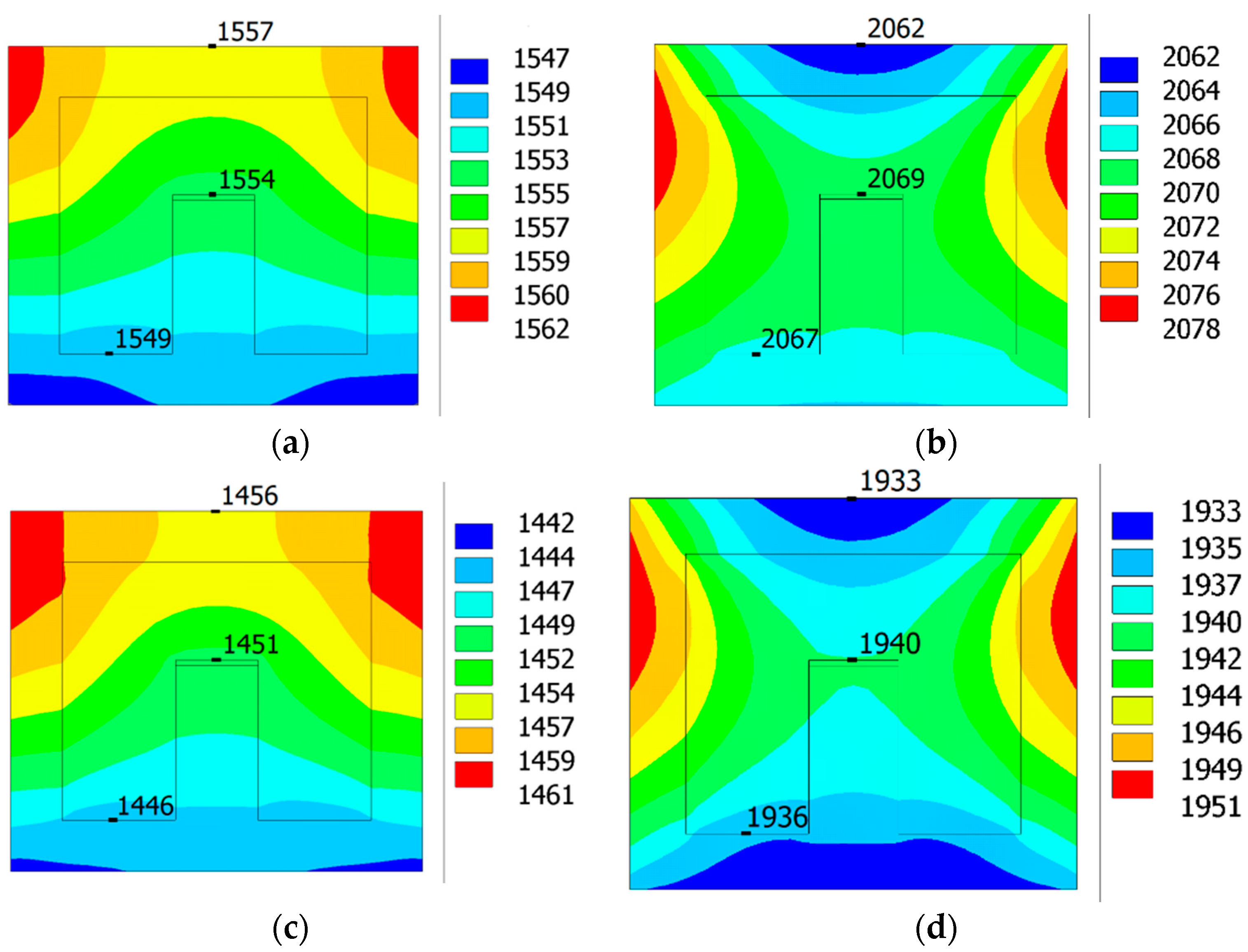
The implementation of the Degussa furnace model, reflecting the details of its construction and the presence of heat transport and exchange phenomena during high-temperature processes, allowed for analysis of the heat distribution in the graphite cassette in the range of the considered pressures and temperatures. In order to use the model for real annealing processes of SiC substrates and the thermal diffusion of dopants in this material, a 10 × 10 mm silicon carbide sample has been introduced to the model in the central part of the graphite cassette. It was modeled assuming ideal thermal contact with heat flux continuity and a lack of heat dissipation. The numerical simulations made on the basis of this model allowed studying the homogeneity of the temperature in the annealed SiC substrate, as well as determining the relationship between the temperature in the most important points of the graphite cassette. Particularly, the relationship between the temperature on the upper surface of the cassette cover, where in real conditions the pyrometric measurement is carried out, and the temperature on the SiC sample placed on the top of the cassette’s bar, were examined. Examples of the results of these simulations are shown in
Figure 10.
The relationship between the simulated temperature T
2 (SiC samples) and the simulated and measured temperature T
1 (upper surface of the cassette) for the operating pressures 1 Pa and 10 kPa is shown in
Table 4. During the actual silicon carbide annealing process, it enables the use of the developed K2 model of the furnace to maintain the temperature of the SiC sample at the assumed level, even though it is not possible to directly measure the temperature of the sample with a pyrometer.
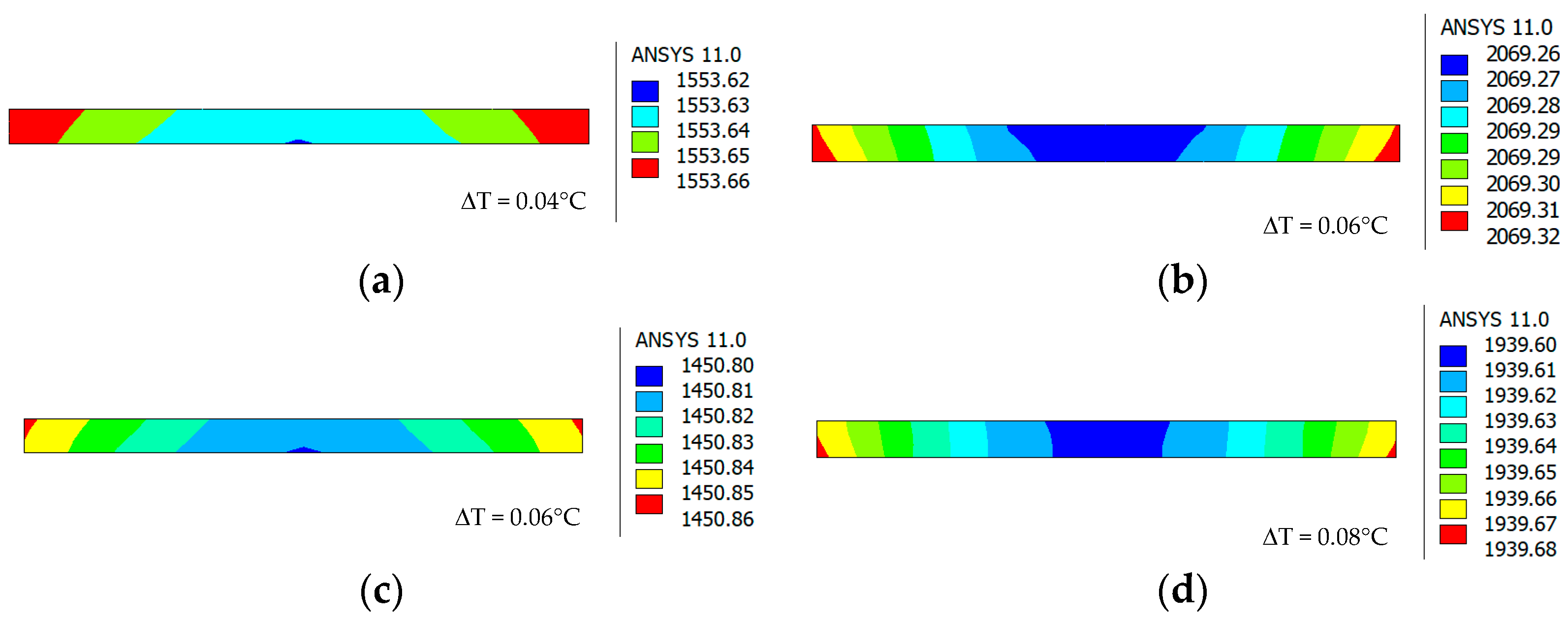
Conducted simulations allowed for the verification of the temperature distribution inside the SiC substrate placed in a closed graphite cassette for different conditions in the annealing process. Exemplary temperature distributions in the SiC sample for low and high temperatures of the cassette, as well as low and high pressure of the surrounding atmosphere, are shown in
Figure 11.
These distributions demonstrated a high homogeneity of temperature over the entire volume of the annealed SiC substrate. The observed temperature differences between the external and central areas of the sample do not exceed the value of 0.1 °C. Obtained results prove that the physical phenomena occurring during the annealing of silicon carbide are of the same nature and intensity on the entire surface of the processed SiC sample and make the results of the applied characterization methods independent from the location of the measurement point.


