
Reconfigurable Low-Density Parity-Check (LDPC) Decoder for Multi-Standard 60 GHz Wireless Local Area Networks


Abstract
:1. Introduction
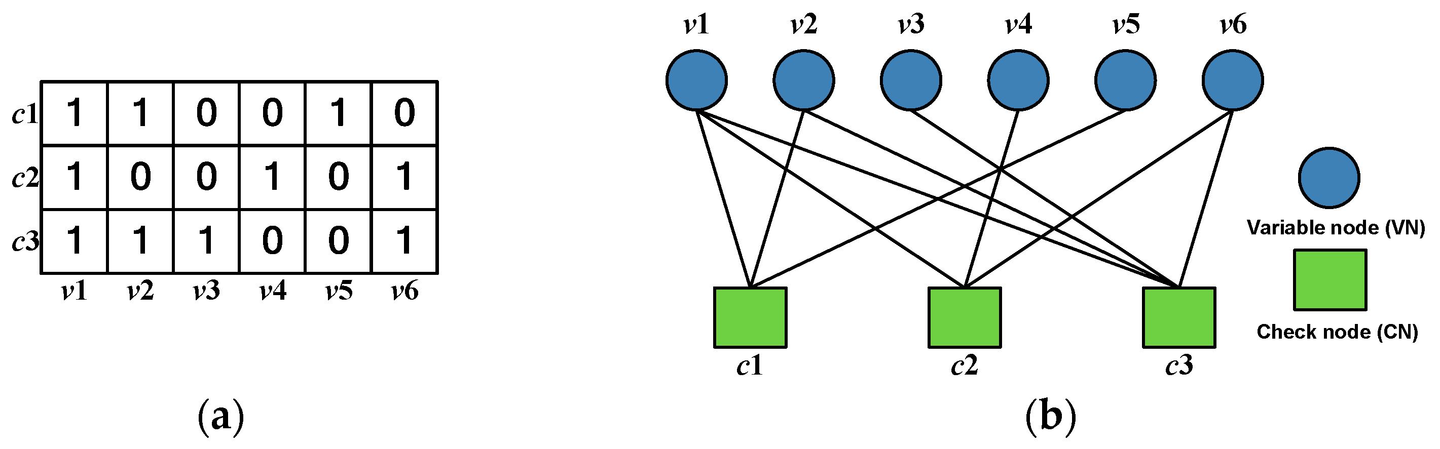
2. Fundamentals of LDPC Code and Decoding
- Initialization:The decoder receives each jth channel message yj to initialise .
- Prior message updates:If k = 1, is updated as and is set to zero.
- CN (extrinsic message) updates:where is a normalisation factor.
- VN (posterior message) updates:
3. Proposed LDPC Decoding for the Multi-Standard 60 GHz Wireless Local Area Networks
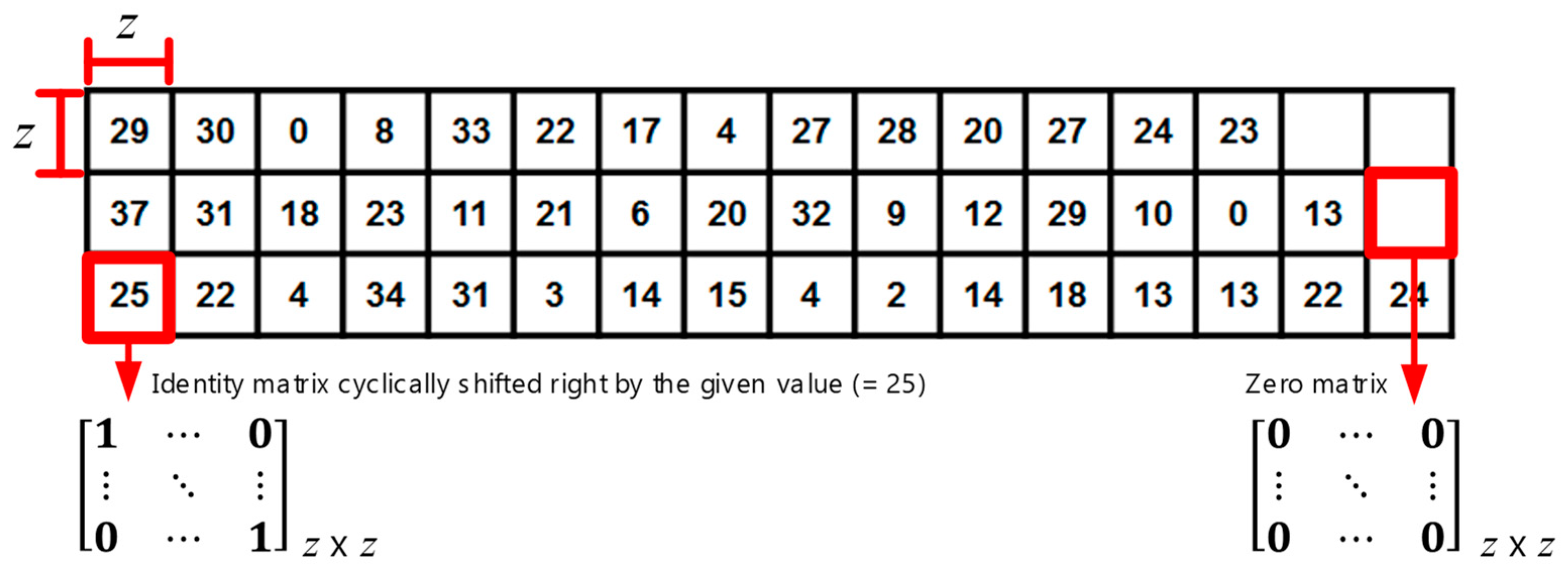
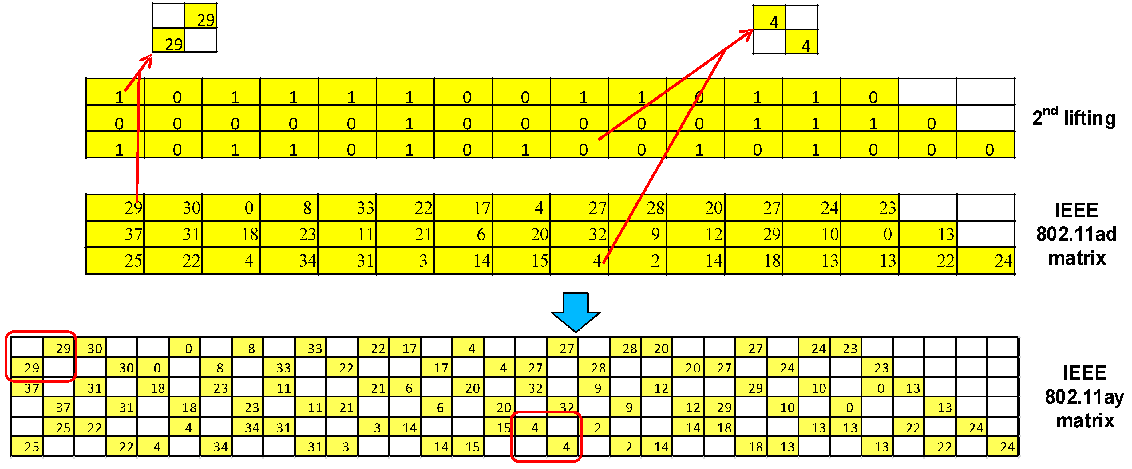
3.1. Standard Parameters and Matrix Configuration
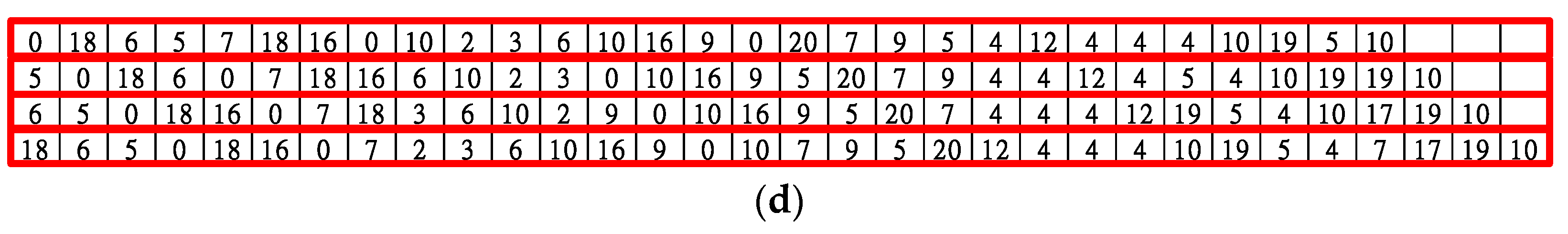
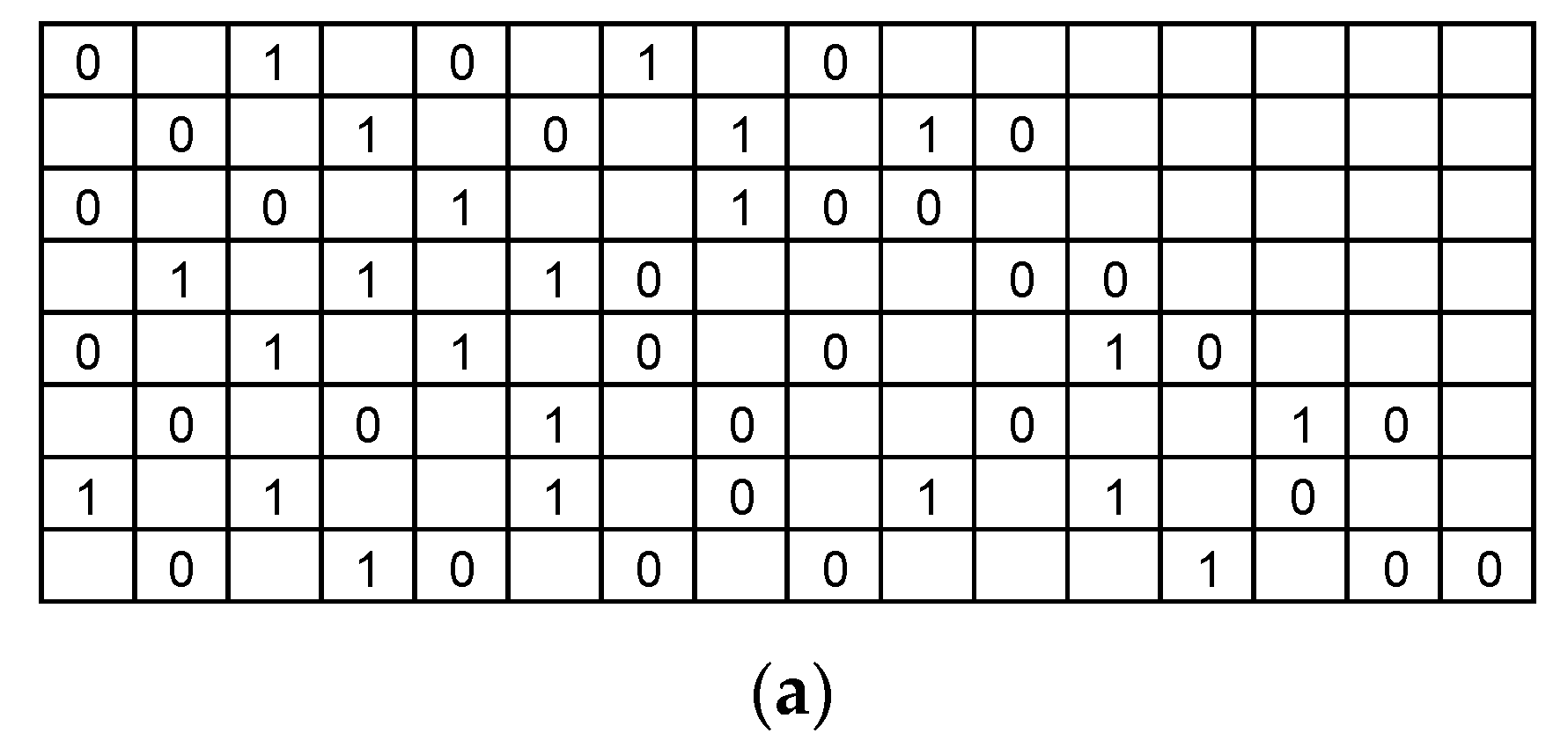
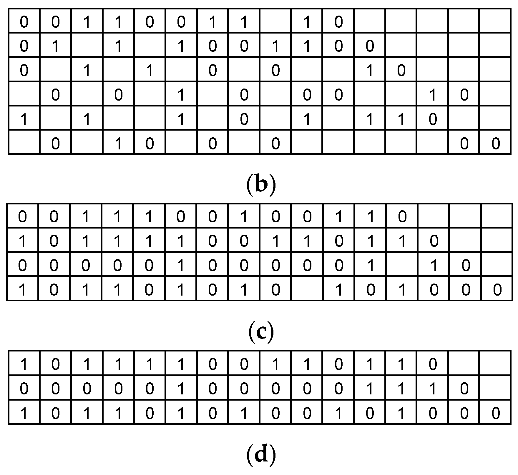
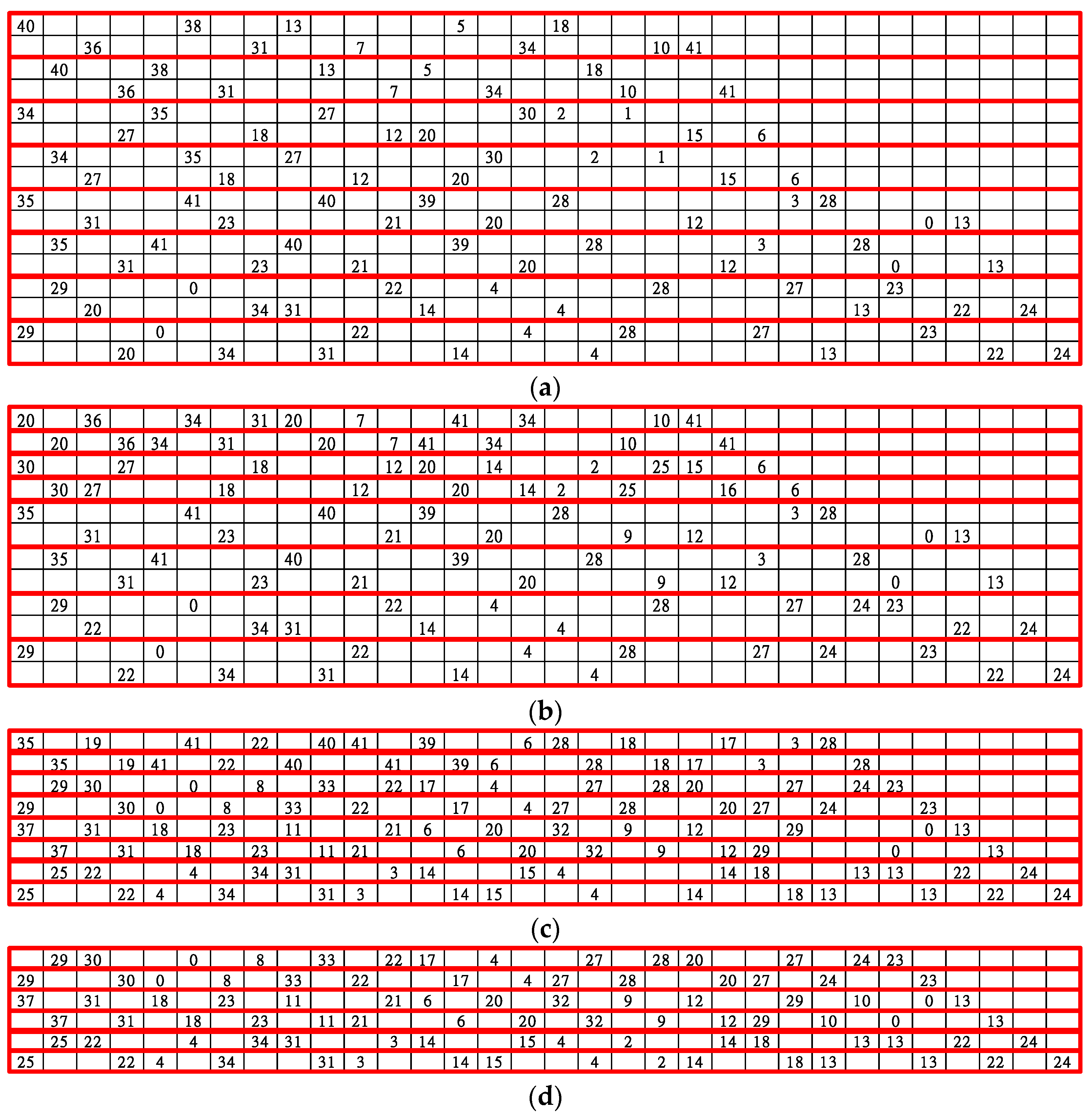
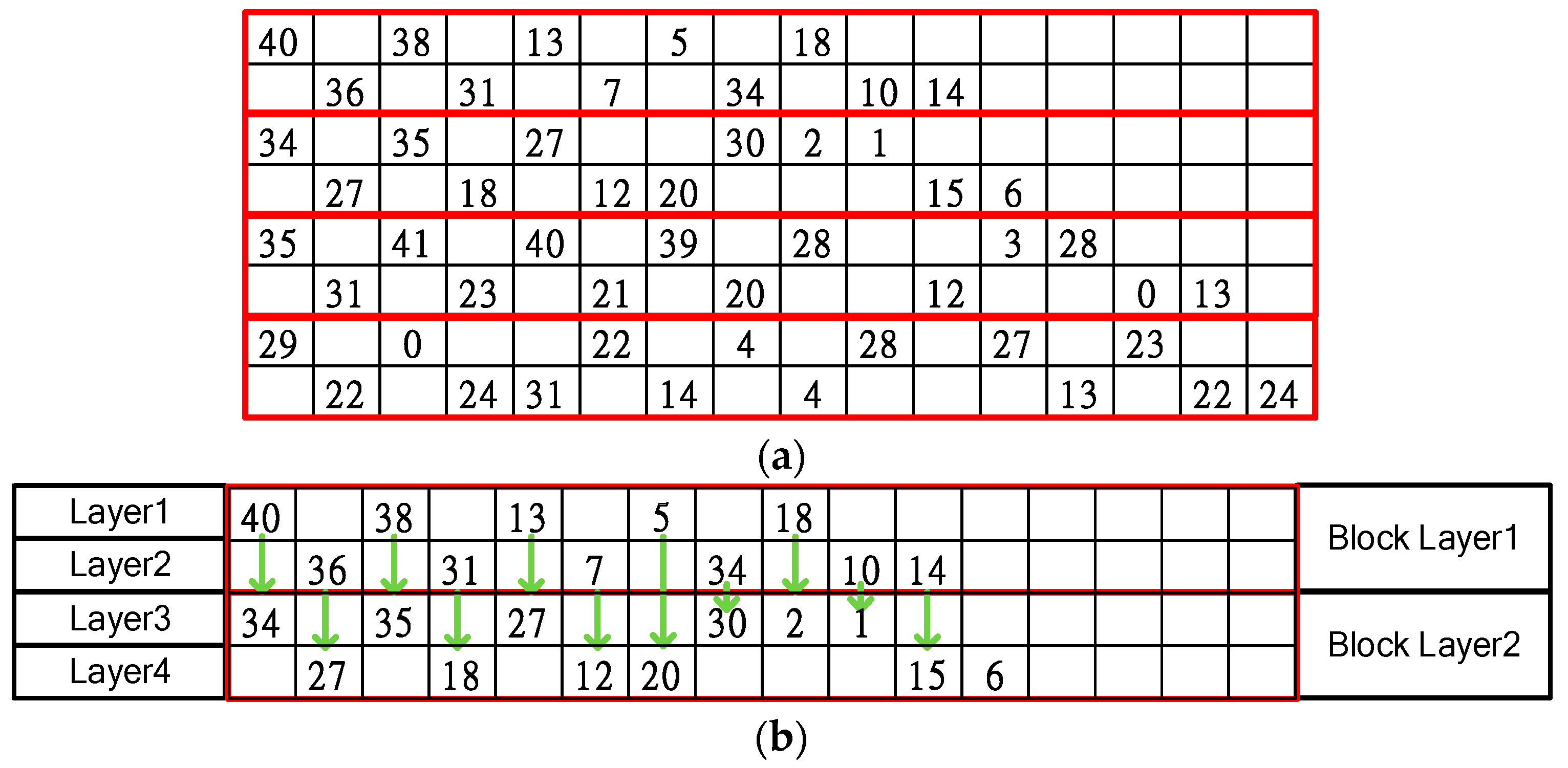
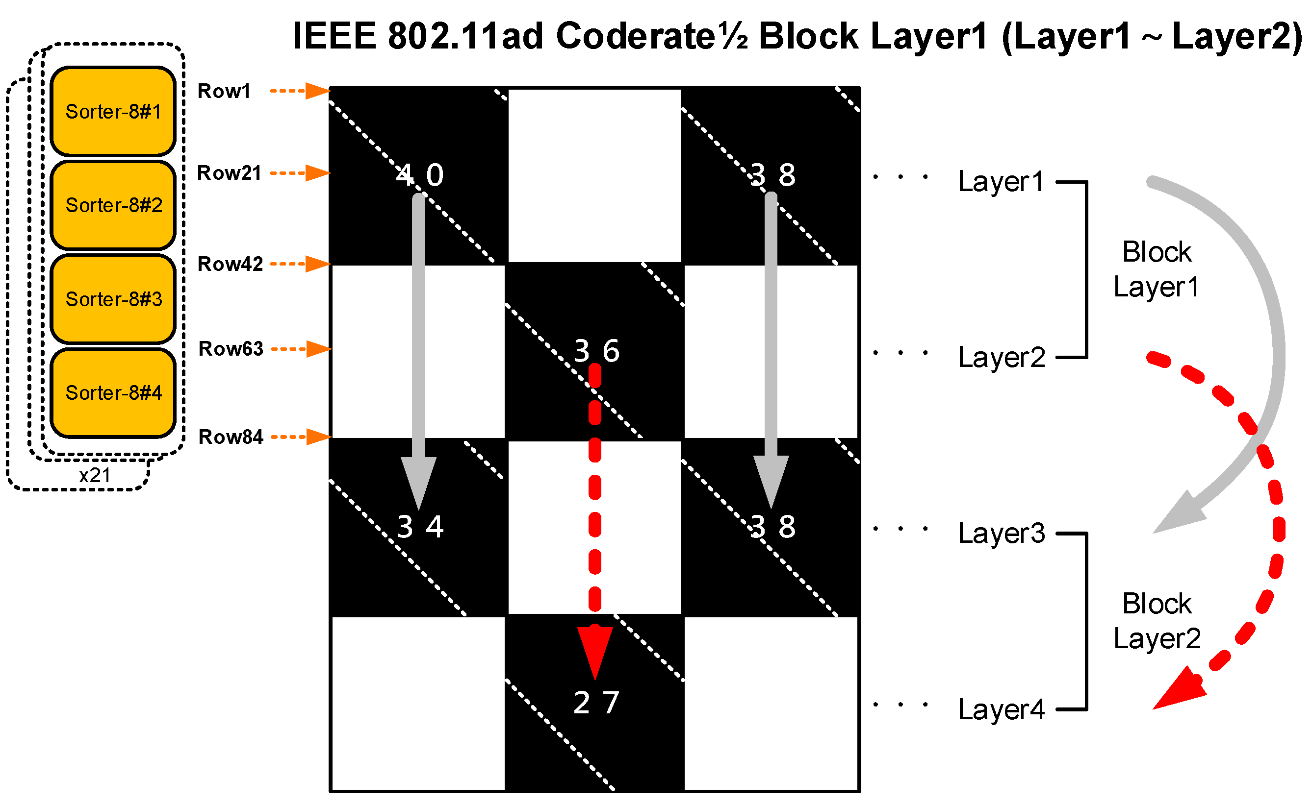
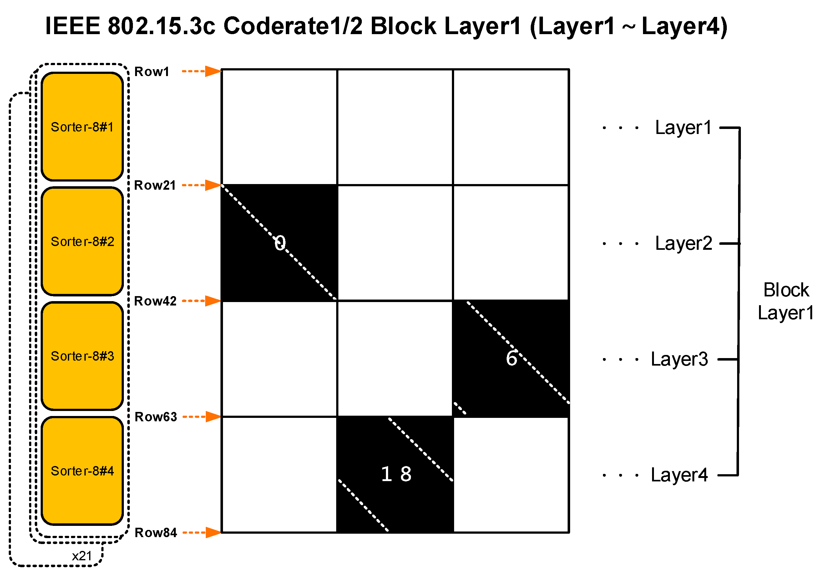
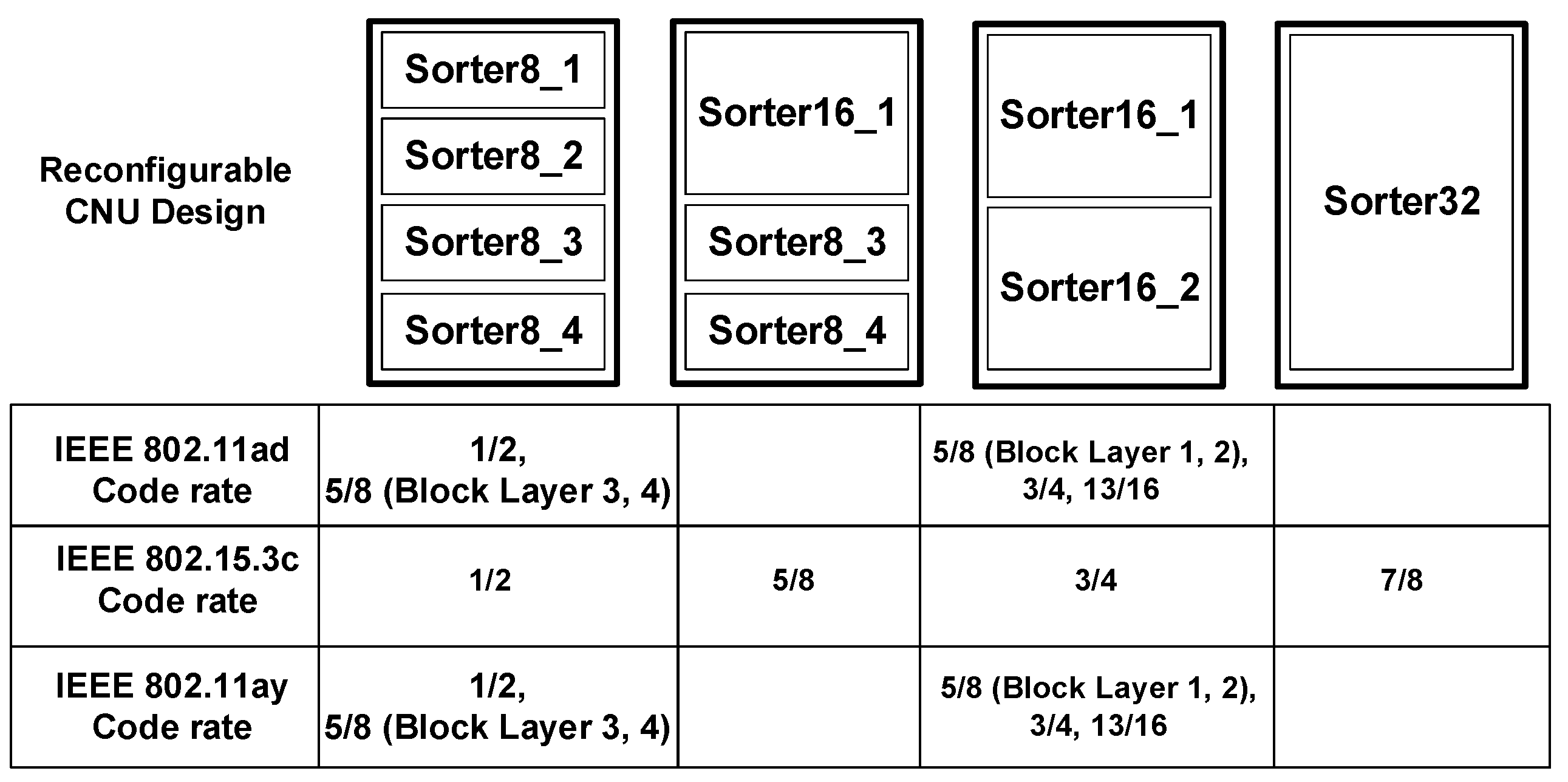
3.2. Proposed Block Layer Decoding for the IEEE 802.11ad, IEEE 802.11ay, and IEEE 802.15.3c Standards
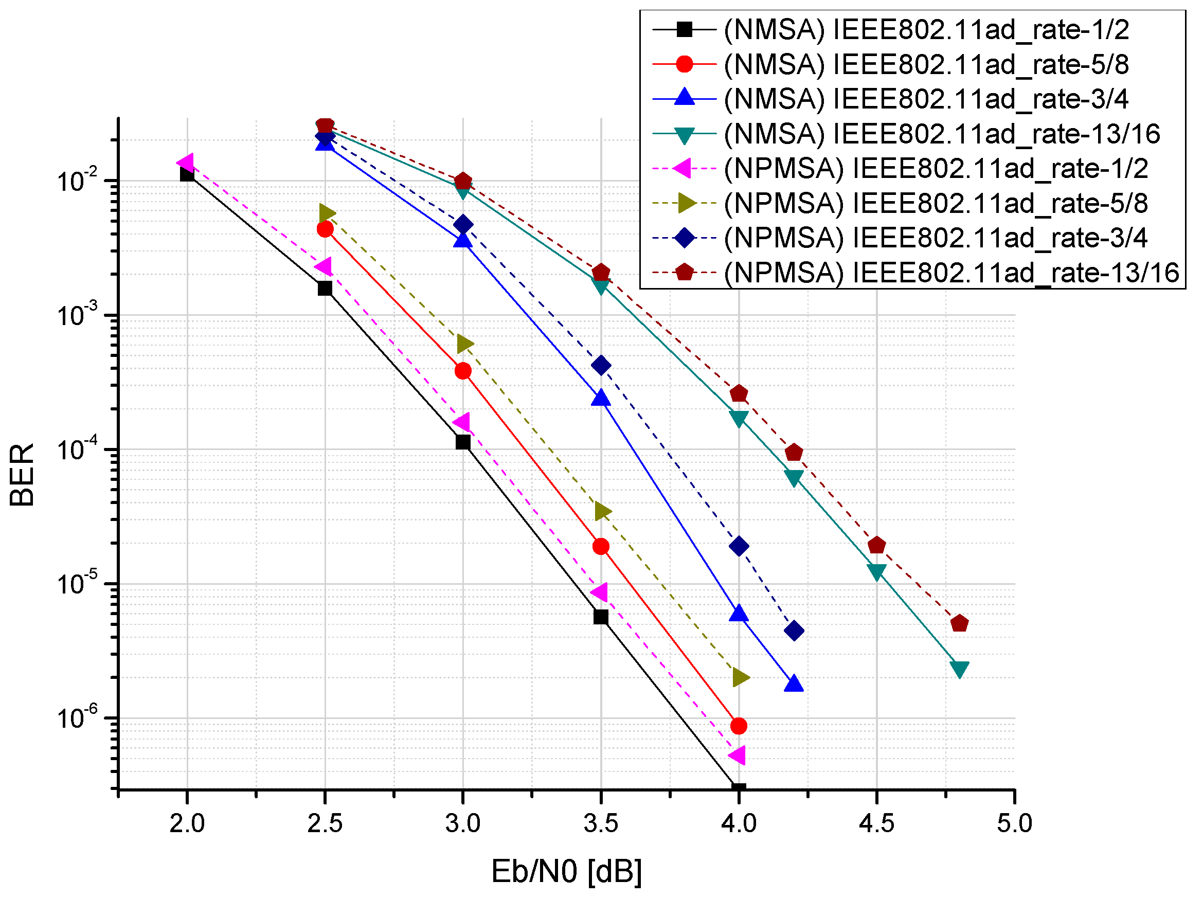
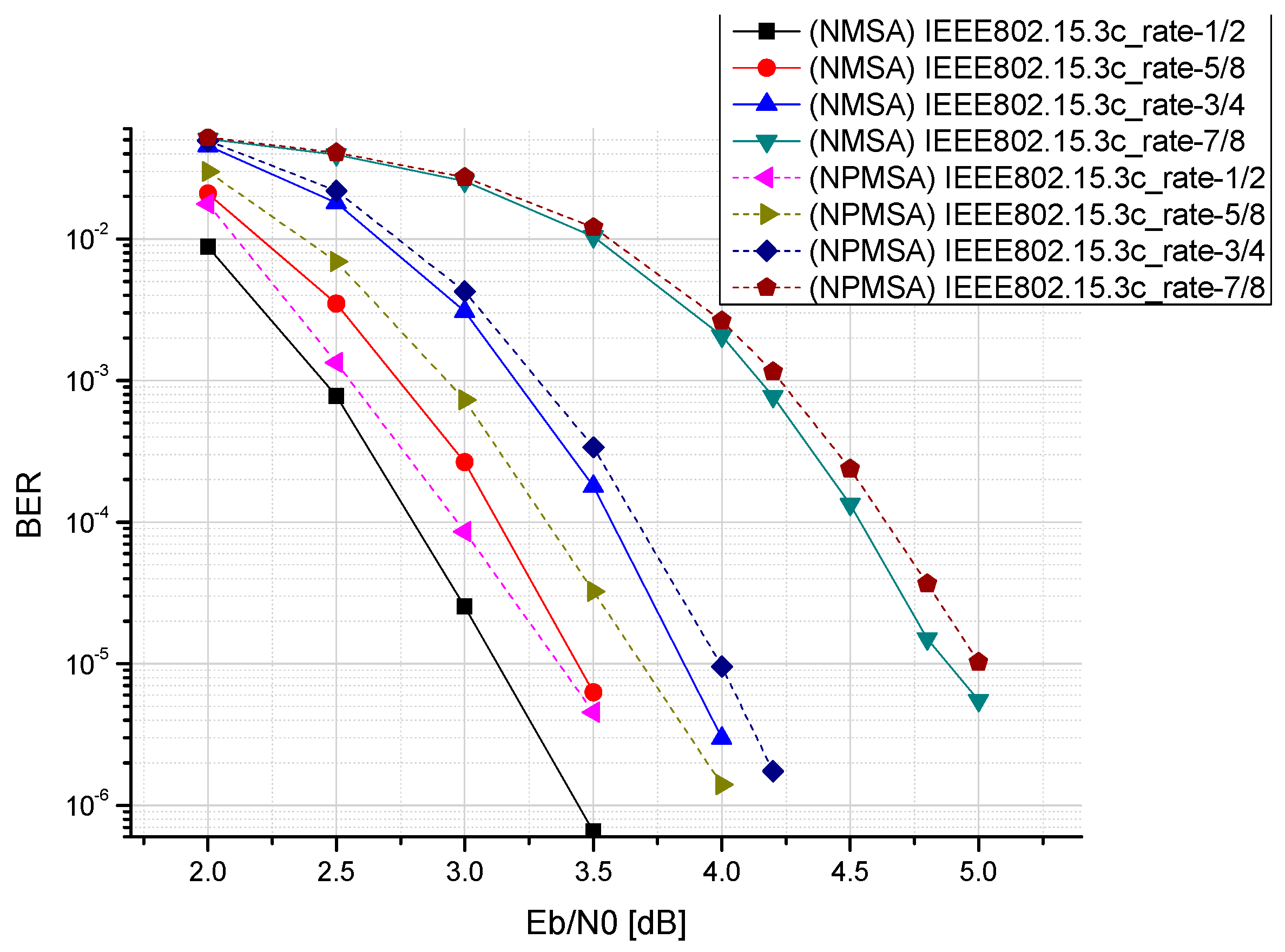
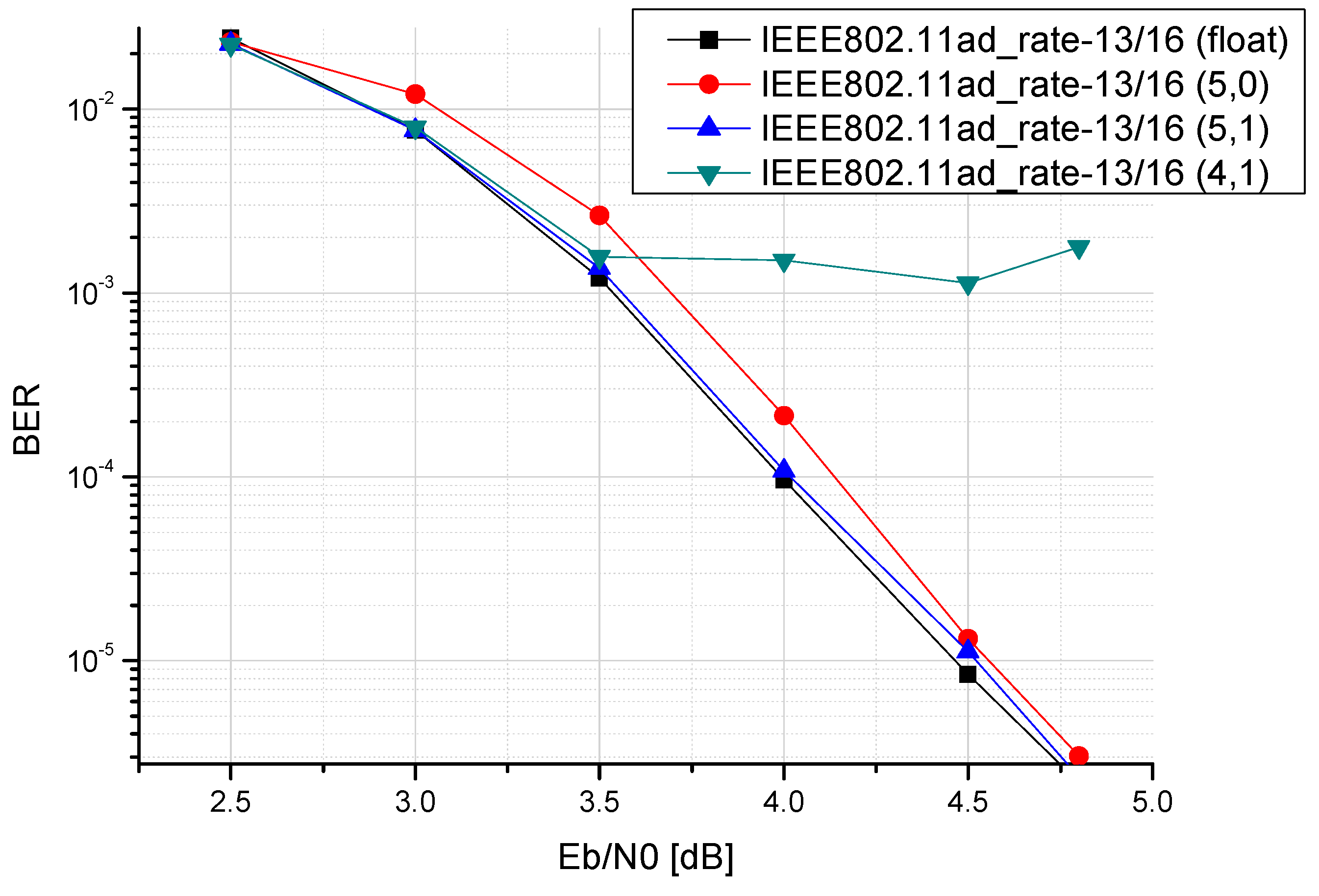
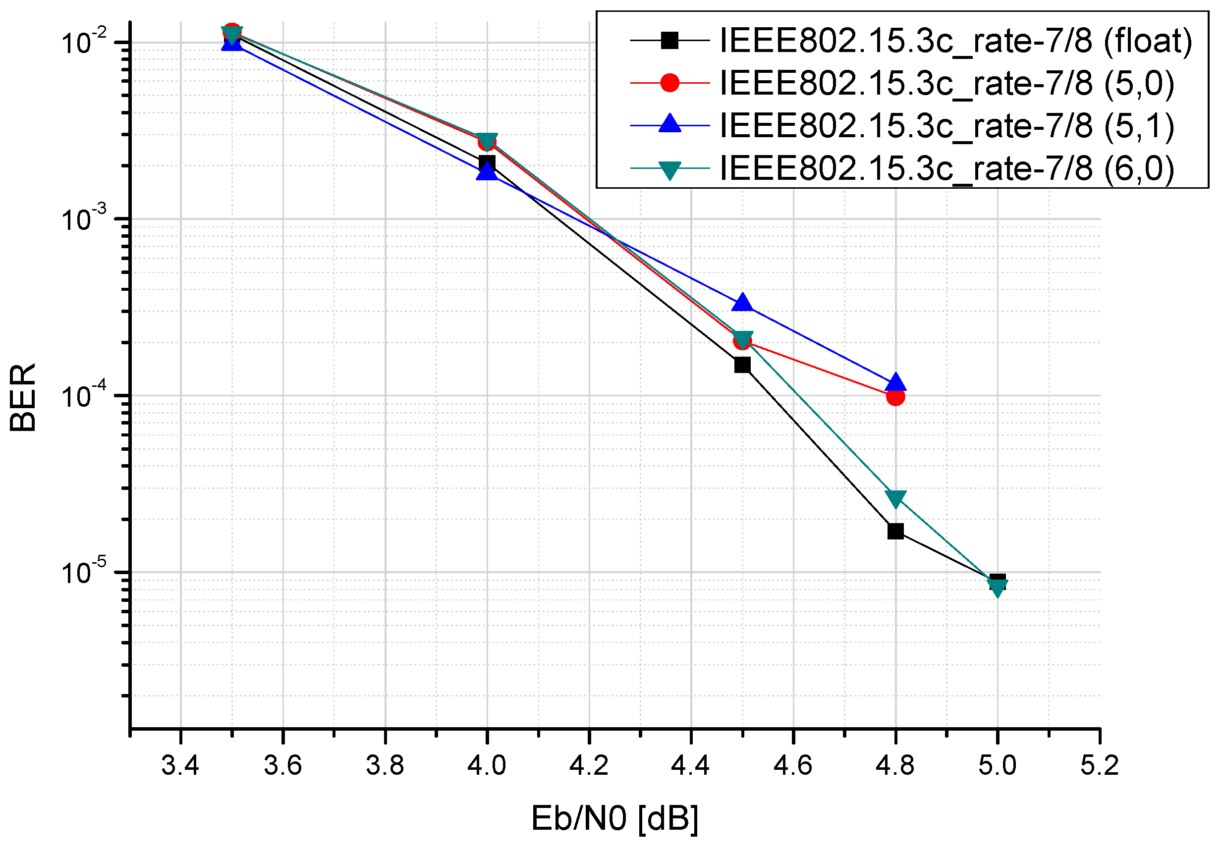
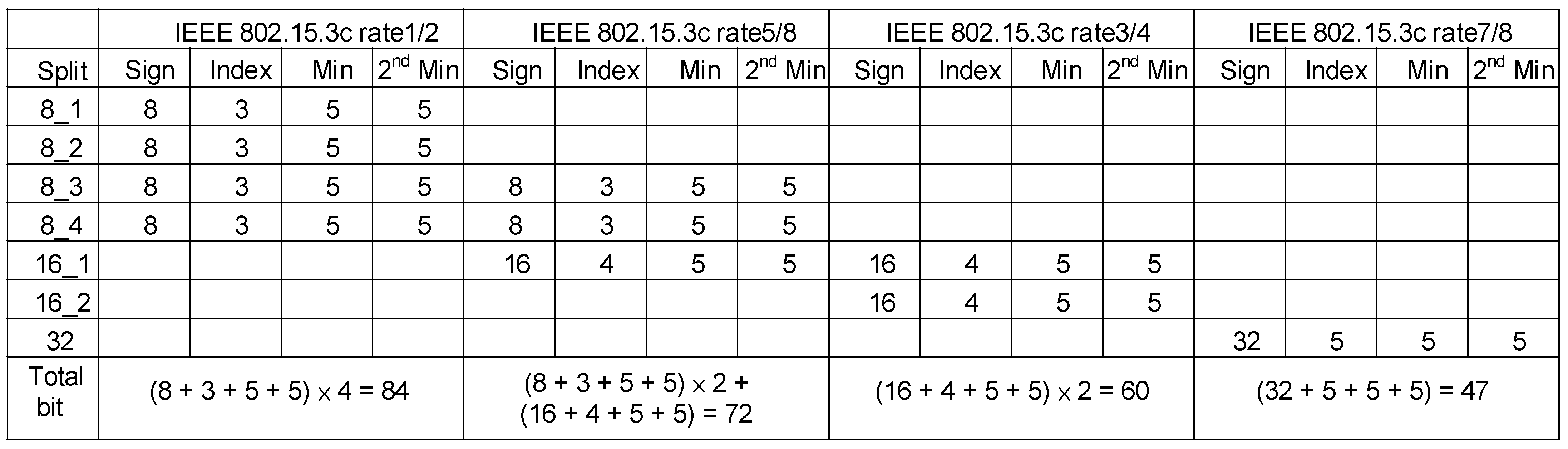
3.3. Finite Word-Lengths of Reconfigurable Multimode LDPC Decoder
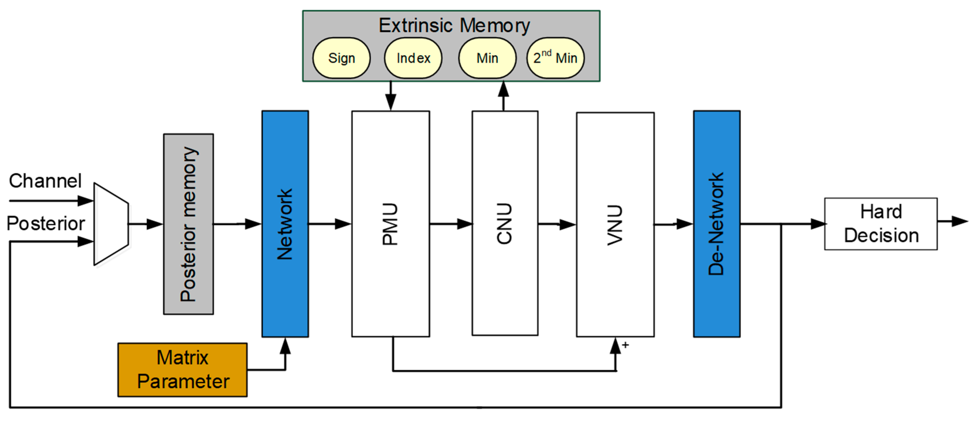
4. Architecture Design of Proposed Reconfigurable Multimode LDPC Decoder
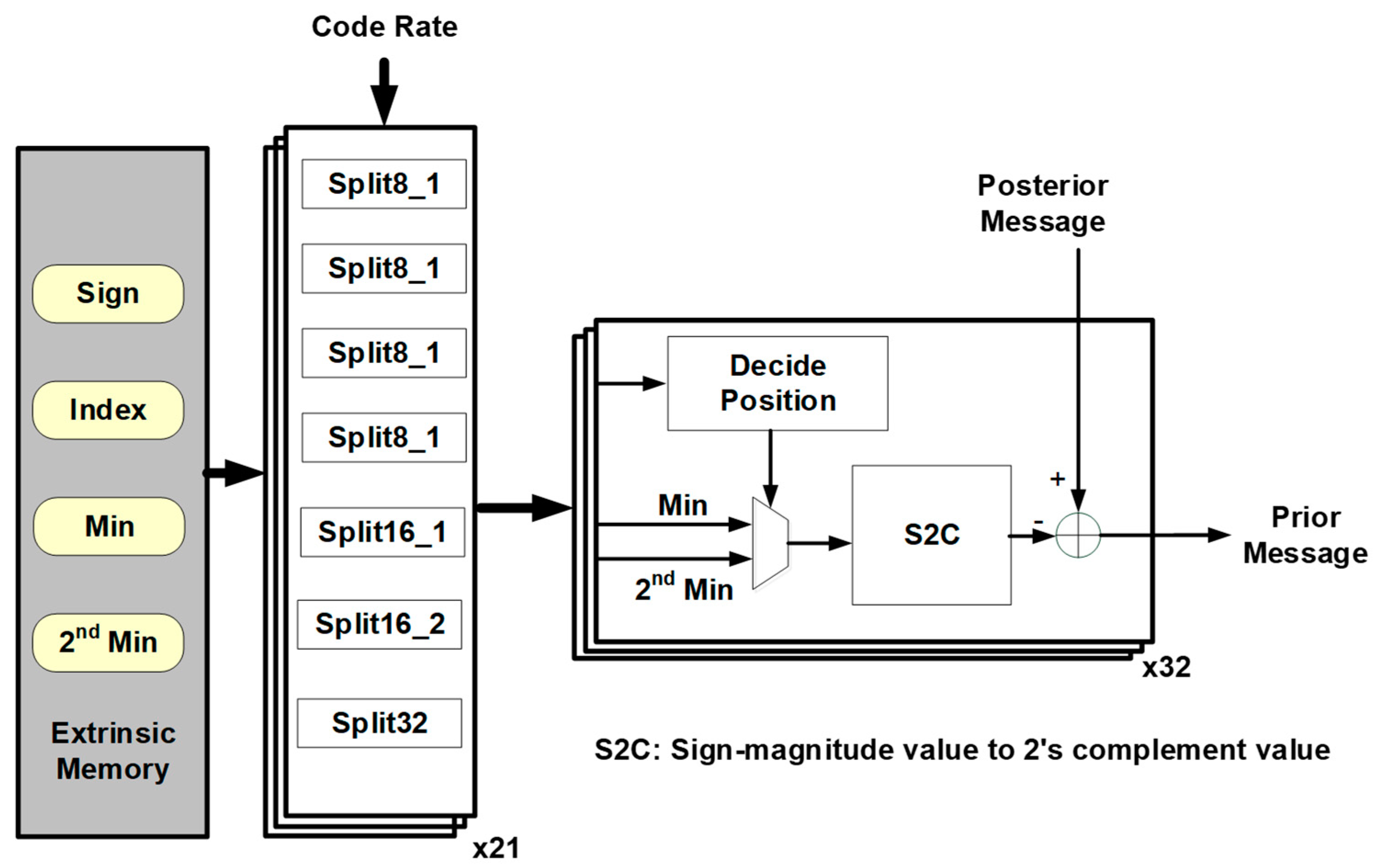
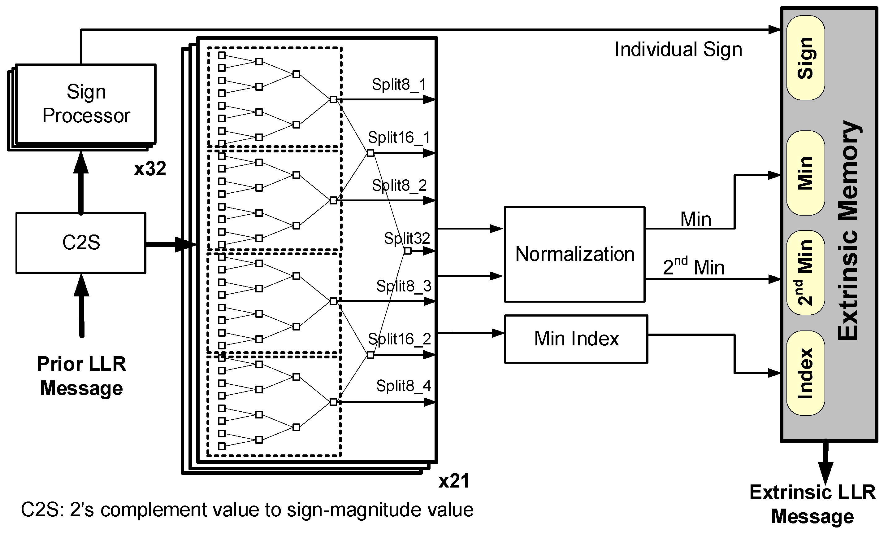
4.1. PMU
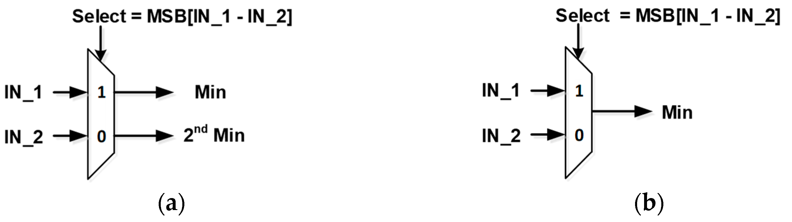
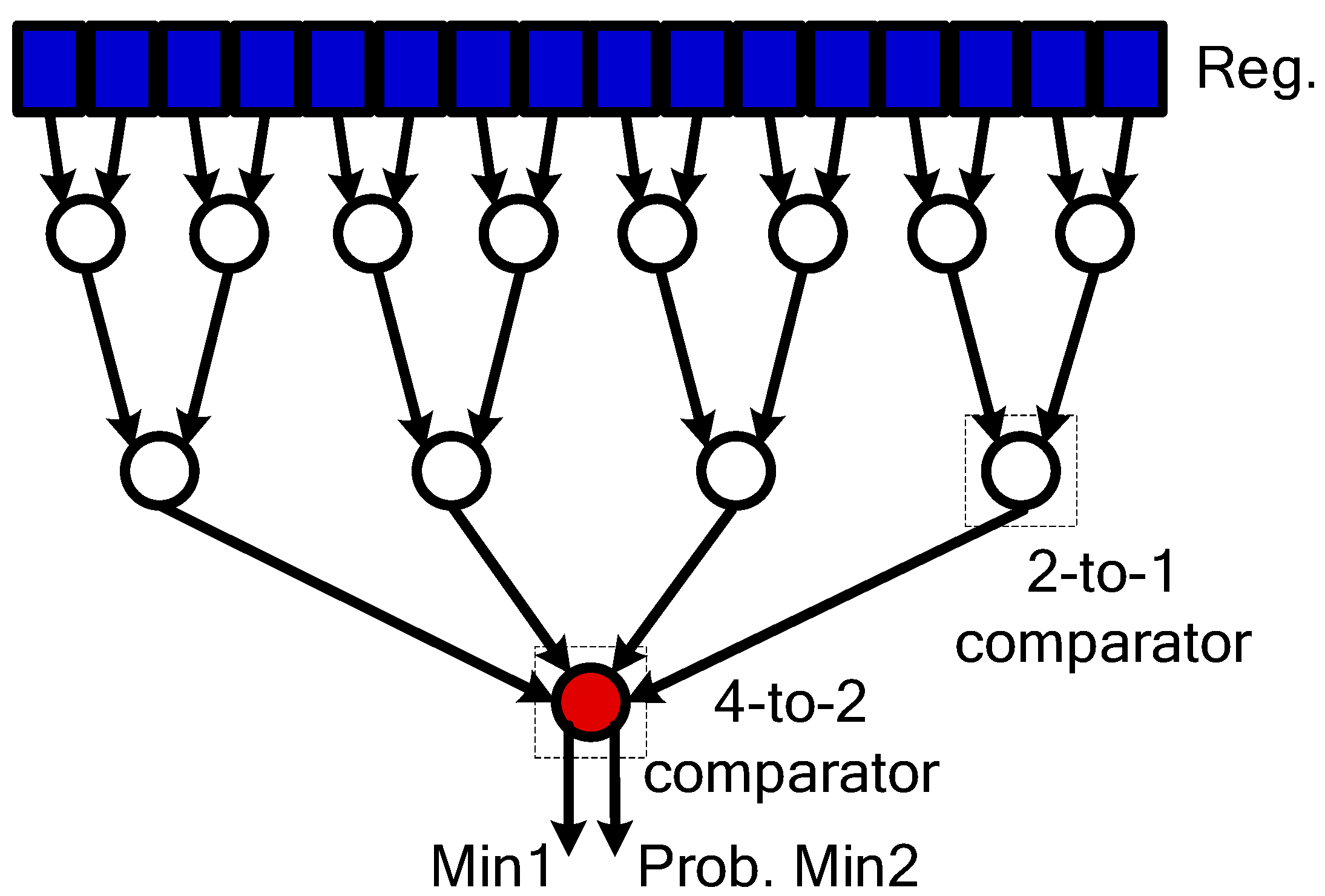
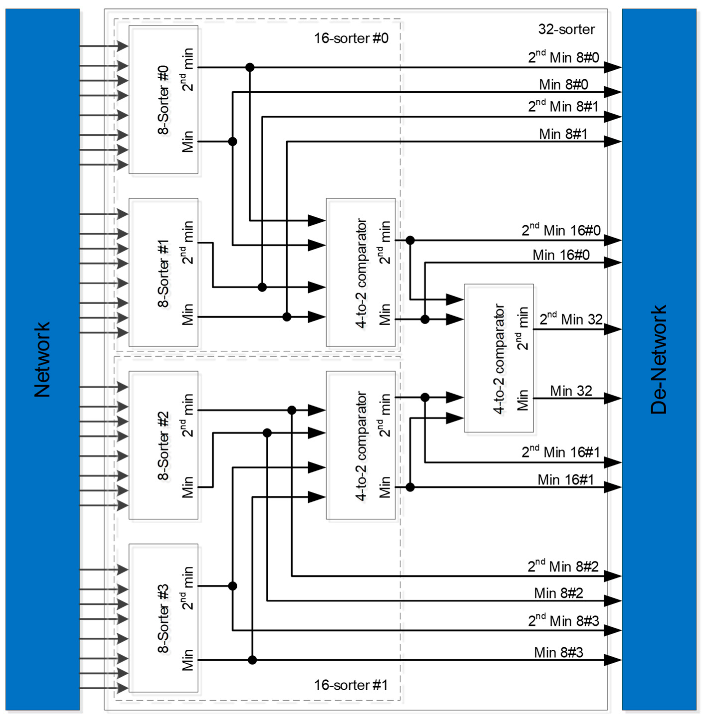
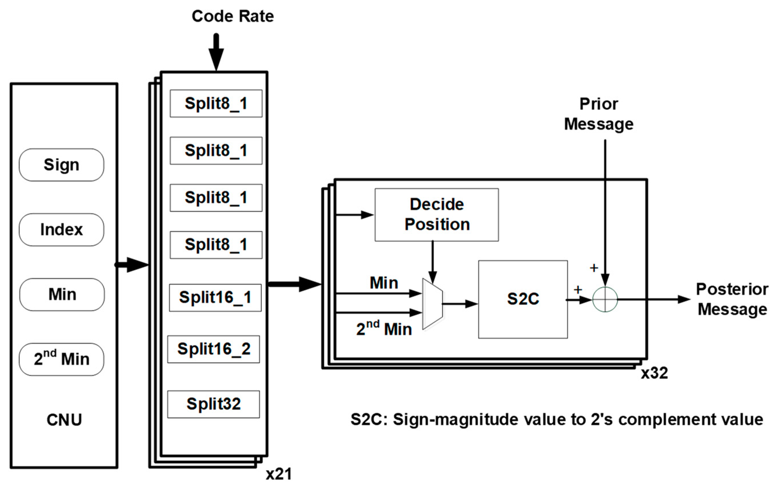
4.2. CNU
4.3. VNU
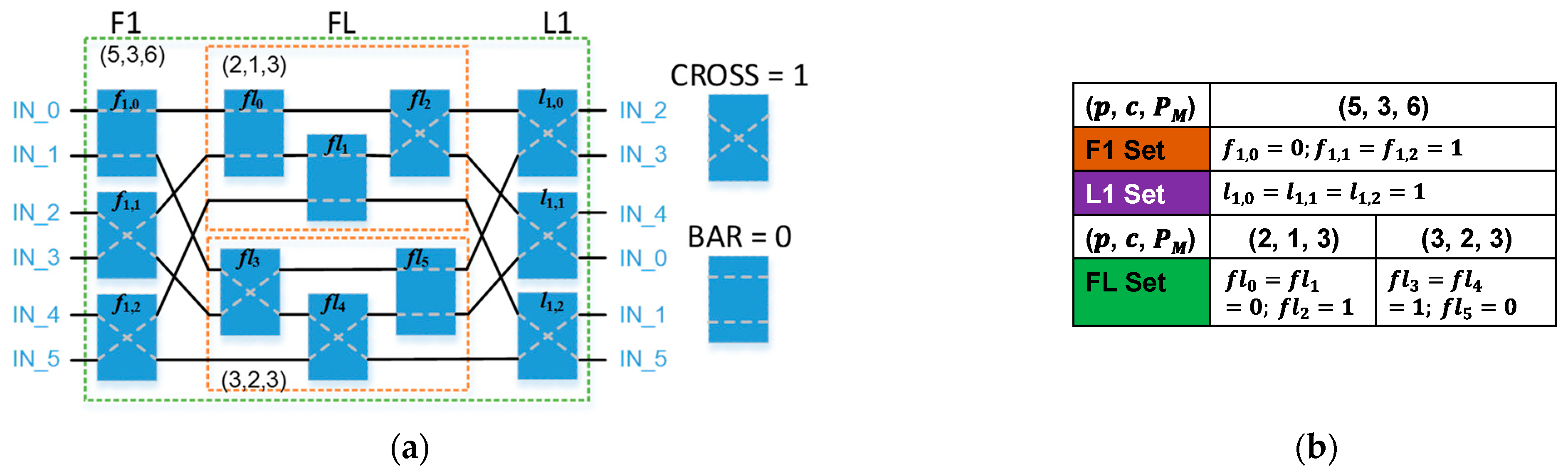
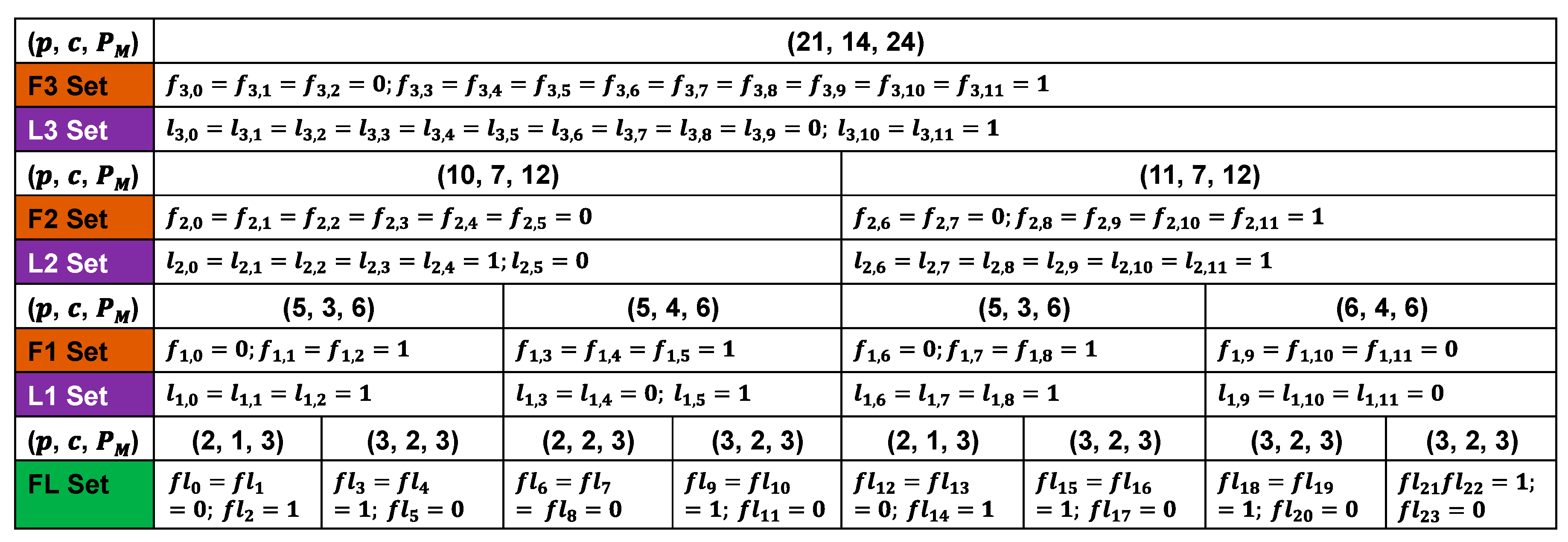
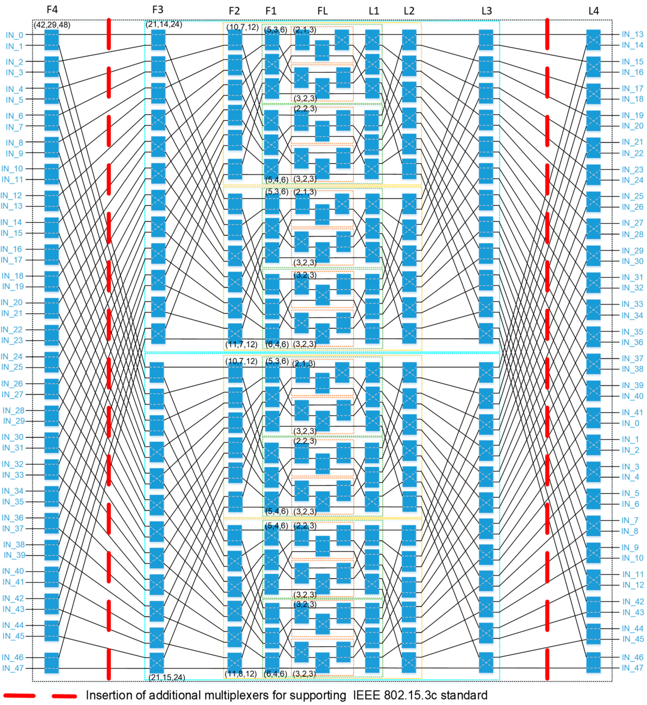
4.4. Switching Network
- The number of inputs may not be a power of 2.
- The number of bits required for the look-up table is very small.
- The hardware usage rate of the proposed multi-mode architecture is extremely high.
4.5. Memory Organization
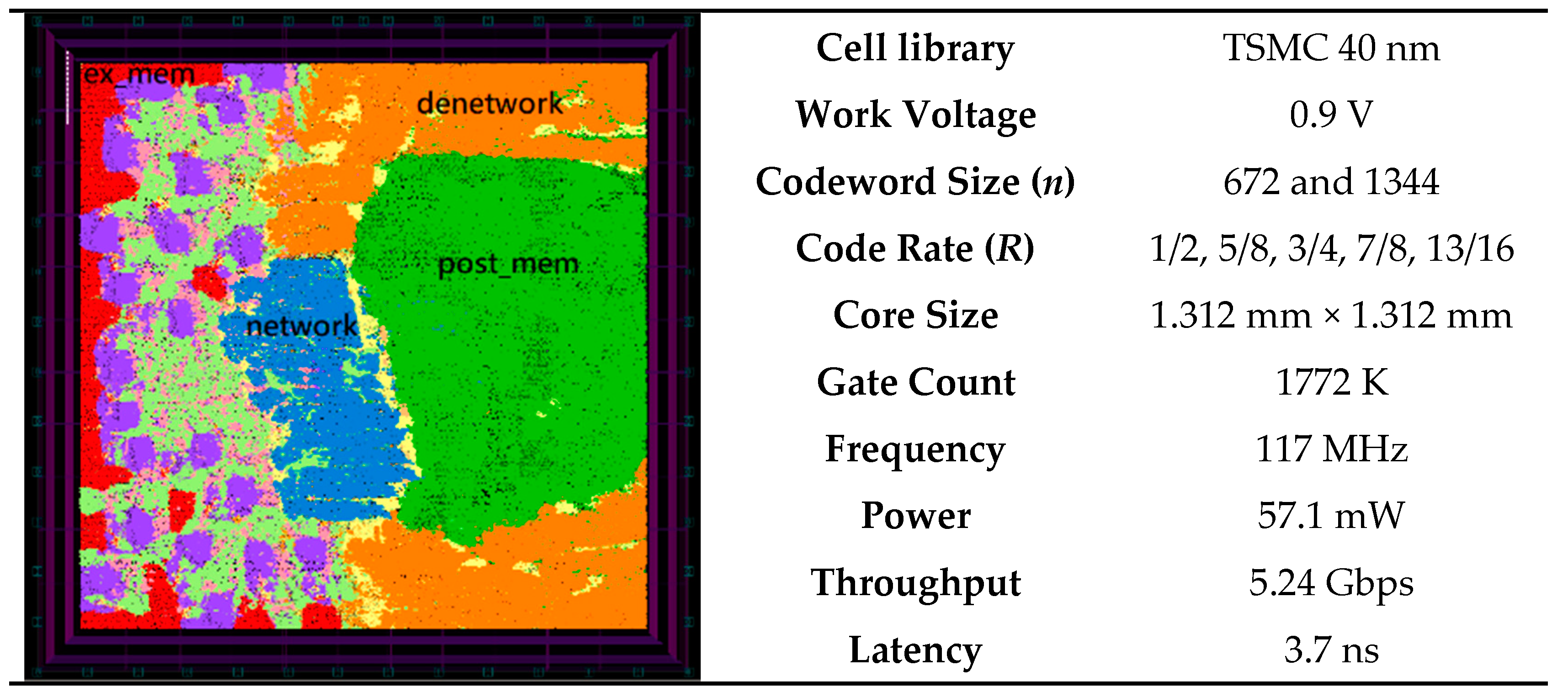
5. VLSI Implementation of Proposed Reconfigurable Multimode LDPC Decoder
6. Conclusions
Author Contributions
Funding
Acknowledgments
Conflicts of Interest
References
- Gallager, R. Low-Density Parity-Check Codes. IEEE Trans. Inform. Theory 1962, 8, 21–28. [Google Scholar] [CrossRef] [Green Version]
- MacKay, D.J.C. Good Error-Correcting Codes Based on Very Sparse Matrices. IEEE Trans. Inform. Theory 1999, 45, 399–431. [Google Scholar] [CrossRef] [Green Version]
- Andriyanov, N.; Dement’ev, V. Topology, Protocols and Databases in Bluetooth 4.0 Sensor Networks. In Proceedings of the 2018 Moscow Workshop on Electronic and Networking Technologies (MWENT), Moscow, Russia, 14–16 March 2018; pp. 1–7. [Google Scholar]
- Singh, R.; Baz, M.; Narayana, C.L.; Rashid, M.; Gehlot, A.; Akram, S.V.; Alshamrani, S.S.; Prashar, D.; AlGhamdi, A.S. Zigbee and Long-Range Architecture Based Monitoring System for Oil Pipeline Monitoring with the Internet of Things. Sustainability 2021, 13, 10226. [Google Scholar] [CrossRef]
- Safaldin, M.; Otair, M.; Abualigah, L. Improved Binary Gray Wolf Optimizer and SVM for Intrusion Detection System in Wireless Sensor Networks. J. Ambient. Intell. Humaniz. Comput. 2021, 12, 1559–1576. [Google Scholar] [CrossRef]
- Khasawneh, A.; Kaiwartya, O.; Abualigah, L.; Lloret, J. Green Computing in Underwater Wireless Sensor Networks Pressure Centric Energy Modeling. IEEE Syst. J. 2020, 14, 4735–4745. [Google Scholar] [CrossRef]
- Otair, M.; Ibrahim, O.T.; Abualigah, L.; Altalhi, M.; Sumari, P. An Enhanced Grey Wolf Optimizer based Particle Swarm Optimizer for Intrusion Detection System in Wireless Sensor Networks. Wirel. Netw. 2022, 28, 721–744. [Google Scholar] [CrossRef]
- Thi Bao Nguyen, T.; Nguyen Tan, T.; Lee, H. Efficient QC-LDPC Encoder for 5G New Radio. Electronics 2019, 8, 668. [Google Scholar] [CrossRef] [Green Version]
- Petrović, V.L.; El Mezeni, D.M.; Radošević, A. Flexible 5G New Radio LDPC Encoder Optimized for High Hardware Usage Efficiency. Electronics 2021, 10, 1106. [Google Scholar] [CrossRef]
- Thi Bao Nguyen, T.; Nguyen Tan, T.; Lee, H. Low-Complexity High-Throughput QC-LDPC Decoder for 5G New Radio Wireless Communication. Electronics 2021, 10, 516. [Google Scholar] [CrossRef]
- Lin, C.-H.; Wang, C.-X.; Lu, C.-K. LDPC Decoder Design Using Compensation Scheme of Group Comparison for 5G Communication Systems. Electronics 2021, 10, 2010. [Google Scholar] [CrossRef]
- Su, H.-H.; Chen, T.-S.; Lin, C.-H. Reconfigurable Check Node Unit Design of Dual-Standard LDPC Decoding for 60GHz Wireless Local Area Network. In Proceedings of the 2019 IEEE International Conference on Consumer Electronics-Taiwan (ICCE-TW), Yilan, Taiwan, 20–22 May 2019; pp. 1–2. [Google Scholar]
- Richardson, T.J.; Urbanke, R.L. Efficient Encoding of Low-Density Parity-Check Codes. IEEE Trans. Inform. Theory 2001, 47, 638–656. [Google Scholar] [CrossRef] [Green Version]
- Roberts, M.K.; Anguraj, P. A Comparative Review of Recent Advances in Decoding Algorithms for Low-Density Parity-Check (LDPC) Codes and Their Applications. Arch. Comput. Methods Eng. 2021, 28, 2225–2251. [Google Scholar] [CrossRef]
- Jinghu Chen, J.; Fossorier, M.P.C. Near Optimum Universal Belief Propagation Based Decoding of Low-Density Parity Check Codes. IEEE Trans. Commun. 2002, 50, 406–414. [Google Scholar] [CrossRef]
- Zhao, J.; Zarkeshvari, F.; Banihashemi, A. On Implementation of Min-Sum Algorithm and Its Modifications for Decoding Low-Density Parity-Check (LDPC) Codes. IEEE Trans. Commun. 2005, 53, 549–554. [Google Scholar] [CrossRef]
- Mansour, M.M.; Shanbhag, N.R. High-throughput LDPC Decoders. IEEE Trans. VLSI Syst. 2003, 11, 976–999. [Google Scholar] [CrossRef] [Green Version]
- Zhang, Z.; Zhou, L.; Zhou, Z.H. Design of A Parallel Decoding Method for LDPC Code Generated via Primitive Polynomial. Electronics 2021, 10, 425. [Google Scholar] [CrossRef]
- Cheng, C.-C.; Yang, J.-D.; Lee, H.-C.; Yang, C.-H.; Ueng, Y.-L. A Fully Parallel LDPC Decoder Architecture Using Probabilistic Min-Sum Algorithm for High-Throughput Applications. IEEE Trans. Circuits Syst. 2014, 61, 2738–2746. [Google Scholar] [CrossRef]
- Tsatsaragkos, I.; Paliouras, V. Approximate Algorithms for Identifying Minima on Min-Sum LDPC Decoders and Their Hardware Implementation. IEEE Trans. Circuits Syst. 2015, 62, 766–770. [Google Scholar] [CrossRef]
- Català-Pérez, J.M.; Lacruz, J.O.; García-Herrero, F.; Valls, J.; Declercq, D. Second Minimum Approximation for Min-Sum Decoders Suitable for High-Rate LDPC Codes. Circuits Syst. Signal Process. 2019, 38, 5068–5080. [Google Scholar] [CrossRef]
- Lin, C.-H.; Wu, Y.-S.; Song, C.-P. Energy-Efficient LDPC Codec Design Using Cost-Effective Early Termination Scheme. IET Comput. Digit. Tech. 2018, 13, 118–125. [Google Scholar] [CrossRef]
- Xiang, B.; Shen, R.; Pan, A.; Bao, D.; Zeng, X. An Area-Efficient and Low-Power Multirate Decoder for Quasi-Cyclic Low-Density Parity-Check Codes. IEEE Trans. VLSI Syst. 2010, 10, 1447–1460. [Google Scholar] [CrossRef]
- Yen, S.W.; Hung, S.Y.; Chen, C.H.; Chang, H.C.; Jou, S.J.; Lee, C.Y. A 5.79-Gigabits per Second Energy-Efficient Multirate LDPC Codec Chip for IEEE 802.15.3c Applications. IEEE J. Solid-State Circuits 2012, 47, 2246–2257. [Google Scholar] [CrossRef]
- Oh, D.; Parhi, K.K. Low-Complexity Switch Network for Reconfigurable LDPC Decoders. IEEE Trans. VLSI Syst. 2010, 18, 85–94. [Google Scholar] [CrossRef]
- Beneš, V.E. Optimal Rearrangeable Multistage Connecting Networks. Bell Syst. Tech. J. 1964, 43, 1641–1656. [Google Scholar] [CrossRef]
- Lin, C.-H.; Hsieh, C.-W. Low-Routing-Complexity Convolutional/Turbo Decoder Design for Iterative Detection and Decoding Receivers. IEEE Trans. Circuits Syst. I Regul. Pap. 2019, 66, 4476–4489. [Google Scholar] [CrossRef]
- Li, M.; Naessens, F.; Debacker, P.; Raghavan, P.; Desset, C.; Li, M.; Dejonghe, A.; Van der Perre, L. An Area and Energy Efficient Half-Row-Paralleled Layer LDPC Decoder for the 802.11Ad Standard. In Proceedings of the 2013 IEEE Workshop on Signal Processing Systems (SiPS), Taipei, Taiwan, 16–18 October 2013; pp. 112–117. [Google Scholar]
- Motozuka, H.; Yosoku, N.; Sakamoto, T.; Tsukizawa, T.; Shirakata, N.; Takinami, K. A 6.16 Gigabits per Second 4.7 pJ/Bit/Iteration LDPC Decoder for IEEE 802.11 ad Standard in 40 nm LP-CMOS. In Proceedings of the 2015 IEEE Global Conference on Signal and Information Processing (GlobalSIP), Orlando, FL, USA, 14–16 December 2015; pp. 1289–1292. [Google Scholar]
- Milicevic, M.; Gulak, P.G. A Multi-Gb/s Frame-Interleaved LDPC Decoder with Path-Unrolled Message Passing in 28-nm CMOS. IEEE Trans. VLSI Syst. 2018, 26, 1908–1921. [Google Scholar] [CrossRef]
- Li, M.; Weijers, J.W.; Derudder, V.; Vos, I.; Rykunov, M.; Dupont, S.; Debacker, P.; Dewilde, A.; Huang, Y.; Van der Perre, L.; et al. An Energy Efficient 18Gigabits per Second LDPC Decoding Processor for 802.11Ad in 28 nm CMOS 2015. In Proceedings of the 2015 IEEE Asian Solid-State Circuits Conference (A-SSCC), Xiamen, China, 9–11 November 2015; pp. 1–5. [Google Scholar]
- Lee, X.; Chen, C.; Chang, H.; Lee, C. A 7.92 Gigabits per Second 437.2 mW Stochastic LDPC Decoder Chip for IEEE 802.15.3c Applications. IEEE Trans. Circuits Syst. 2015, 62, 507–516. [Google Scholar] [CrossRef]
- Chen, Z.; Peng, X.; Zhao, X.; Okamura, L.; Zhou, D.; Goto, S. A 6.72-Gigabits per Second 8 pJ/Bit/Iteration IEEE 802.15.3c LDPC Decoder Chip. IEICE Trans. Fundam. Electron. Commun. Comput. Sci. 2013, 96, 2623–2632. [Google Scholar] [CrossRef]
- Li, M.-R.; Yang, C.-H.; Ueng, Y.-L. A 5.28-Gigabits per Second LDPC Decoder with Time-Domain Signal Processing for IEEE 802.15.3c Applications. IEEE J. Solid-State Circuits 2017, 52, 592–604. [Google Scholar] [CrossRef]


| Application | WiHD | WiGig | |
|---|---|---|---|
| Transmission standard | IEEE 802.15.3c | IEEE 802.11ad | IEEE 802.11ay |
| Working frequency | 60 GHz | 60 GHz | 60 GHz |
| FEC code | LDPC codes (Code rate: 1/2–7/8) | LDPC codes (Rate 1/2–13/16) | LDPC codes (Rate 1/2–13/16) |
| Theoretical transmission rate | 10~28 Gbps | 7~28 Gbps | 20~100 Gbps |
| Standards | IEEE 802.11ay | IEEE 802.11ad | IEEE 802.15.3c | |||||||||
|---|---|---|---|---|---|---|---|---|---|---|---|---|
| Rate | 1/2 | 5/8 | 3/4 | 13/16 | 1/2 | 5/8 | 3/4 | 13/16 | 1/2 | 5/8 | 3/4 | 7/8 |
| Row | 16 | 12 | 8 | 6 | 8 | 6 | 4 | 3 | 16 | 12 | 8 | 4 |
| Column | 32 | 32 | 32 | 32 | 16 | 16 | 16 | 16 | 32 | 32 | 32 | 32 |
| Expansion factor | 42 | 42 | 42 | 42 | 42 | 42 | 42 | 42 | 21 | 21 | 21 | 21 |
| Code length | 1344 | 1344 | 1344 | 1344 | 672 | 672 | 672 | 672 | 672 | 672 | 672 | 672 |
| Row weight | 8 | 10 | 15 | 16 | 8 | 10 | 15 | 16 | 8 | 15 | 16 | 32 |
| Network | Benes Network [26] | This Work |
|---|---|---|
| Network size | ||
| Look-up table (bits) | 709,984 (100%) | 588 (0.08%) |
| Decoders | This Study | [28] | [29] | [30] | [31] |
|---|---|---|---|---|---|
| Implementation | Post-layout | Measurement | Measurement | Measurement | Measurement |
| Technology | 40 nm | 40 nm | 40 nm | 28 nm | 28 nm |
| Voltage | 0.9 V | 0.9 V | 1.1 V | 0.9 V | 0.9 V |
| Standard | IEEE 802.11ad/ay IEEE 802.15.3c | IEEE 802.11ad | IEEE 802.11ad | IEEE 802.11ad | IEEE 802.11ad |
| Code rate (R) | 1/2, 5/8, 3/4 7/8, 13/16 | 13/16 | 1/2, 5/8, 3/4, 13/16 | 1/2, 5/8, 3/4, 13/16 | 1/2, 5/8, 3/4, 13/16 |
| Algorithm | NPMSA | MSA | MSA | MSA | MSA |
| Quantization (bits) | 7 | 5 | 5 | 5 | 4 |
| Iteration | 5 | 5 | 7 | 10 | 4 |
| Parallelism | 21 | 42 | 16 | 168 | 42 |
| Frequency (MHz) | 117 | 500 | 220 | 202 | 470 |
| Tp (Gbps) | 5.24 | 5.6 | 6.16 | 6.78 | 18.4 |
| Area (mm2) | 1.72 | 0.16 | 0.8 | 1.99 | 0.78 |
| Power (mW) | 57.1 | 99 | 203 | 104 | 166 |
| NAE (bits/mm2) | 0.026 | 0.07 | 0.035 | 0.0082 | 0.024 |
| NEE (pJ/bit) | 2.179 | 3.53 | 3.15 | 2.19 | 3.22 |
| Decoders | This Study | [32] | [33] | [34] | [24] |
|---|---|---|---|---|---|
| Implementation | Post-layout | Measurement | Measurement | Measurement | Measurement |
| Technology | 40 nm | 90 nm | 65 nm | 90 nm | 65 nm |
| Voltage | 0.9 V | 1.2 V | 1.2 V | 1.05 V | 1.0 V |
| Standard | IEEE 802.11ad/ay IEEE 802.15.3c | IEEE 802.15.3c | IEEE 802.15.3c | IEEE 802.15.3c | IEEE 802.15.3c |
| Code rate | 1/2, 5/8, 3/4 7/8, 13/16 | 1/2, 5/8, 3/4, 7/8, | 1/2, 5/8, 3/4, 7/8, | 1/2, 5/8, 3/4, 7/8, | 1/2, 5/8, 3/4, 7/8, |
| Algorithm | NPMSA | NMSA | NMSA | NMSA | NMSA |
| Quantization (bits) | 7 | 10 | 6 | 6 | 6 |
| Iteration | 5 | 10 | 10 | 5 | 5 |
| Parallelism | 21 | 21 | 21 | 21 | 21 |
| Frequency (MHz) | 117 | 768 | 400 | 157 | 197 |
| Tp (Gbps) | 3.90 | 7.92 | 6.72 | 5.28 | 5.79 |
| Area (mm2) | 1.72 | 2.67 | 1.3 | 2.25 | 1.56 |
| Power (mW) | 57.1 | 437.2 | 537.6 | 182 | 361 |
| NAE (bits/mm2) | 0.019 | 0.019 | 0.034 | 0.075 | 0.049 |
| NEE (pJ/bits) | 2.92 | 1.98 | 2.76 | 2.25 | 6.21 |
Publisher’s Note: MDPI stays neutral with regard to jurisdictional claims in published maps and institutional affiliations. |
© 2022 by the authors. Licensee MDPI, Basel, Switzerland. This article is an open access article distributed under the terms and conditions of the Creative Commons Attribution (CC BY) license (https://creativecommons.org/licenses/by/4.0/).
Share and Cite
Lin, C.-H.; Su, H.-H.; Chen, T.-S.; Lu, C.-K. Reconfigurable Low-Density Parity-Check (LDPC) Decoder for Multi-Standard 60 GHz Wireless Local Area Networks. Electronics 2022, 11, 733. https://doi.org/10.3390/electronics11050733
Lin C-H, Su H-H, Chen T-S, Lu C-K. Reconfigurable Low-Density Parity-Check (LDPC) Decoder for Multi-Standard 60 GHz Wireless Local Area Networks. Electronics. 2022; 11(5):733. https://doi.org/10.3390/electronics11050733
Chicago/Turabian StyleLin, Cheng-Hung, Hsin-Hao Su, Tang-Syun Chen, and Cheng-Kai Lu. 2022. "Reconfigurable Low-Density Parity-Check (LDPC) Decoder for Multi-Standard 60 GHz Wireless Local Area Networks" Electronics 11, no. 5: 733. https://doi.org/10.3390/electronics11050733
APA StyleLin, C.-H., Su, H.-H., Chen, T.-S., & Lu, C.-K. (2022). Reconfigurable Low-Density Parity-Check (LDPC) Decoder for Multi-Standard 60 GHz Wireless Local Area Networks. Electronics, 11(5), 733. https://doi.org/10.3390/electronics11050733