1. Introduction
Integrated circuits (ICs) can experience various functionality issues when subjected to prolonged doses of radiation. These effects are often a reliability concern in long-term space missions where devices can spend years exposed to constant sources of radiation. Total ionizing dose (TID) effects in ICs can result in changes to gate propagation delays, leakage currents, and even loss of device functionality [
1]. When ICs are exposed to ionizing radiation, positive charges are accumulated within the gate oxide and field oxide layers, thus resulting in less gate control of the device and an increased leakage current [
2]. For PMOS transistors, the result of these charges can result in the device failing to turn on, whereas NMOS transistors become difficult to turn off [
1,
2]. The mechanisms of TID effects in bulk technologies are often simpler due to the inclusion of only one gate oxide layer; however, fully depleted silicon on insulator (FD SOI) technologies feature a more complex response to TID effects [
3].
Transistors in the latest FD SOI technologies are fabricated on a very thin silicon (Si) layer over a buried oxide layer (BOX). With each transistor fabricated on a Si Island and isolated from other transistors by the BOX layer, the volume of active Si is minimal for each transistor. This allows for superior gate control over the channel region while reducing nodal capacitances, which yields faster logic gate switching times over those for bulk technologies. However, because FD SOI technologies have an additional parasitic structure due to the BOX layer, effects due to TID are more complex than bulk devices [
4,
5,
6,
7,
8,
9]. The BOX layer introduces a two-dimensional coupling effect between the front and back interfaces of the channel. This doubled coupling becomes a critical contribution to the ionizing dose response of FD SOI devices. In this case, FD SOI technologies tend to be more sensitive to TID than their bulk counterparts [
10,
11]. This is important to note due to the attractiveness of FD SOI technologies for use in space missions because of the technologies’ inherent resilience to particle-induced single event effects (SEEs) [
3,
9]. There are already some experimental results from previous research on TID effects in the 28-nm FD SOI technology node [
2,
9]. These results show that a TID-induced gate delay increased significantly in that technology node, as well as leakage currents which impose barriers for it to be used for some space applications where tolerance to high total absorbed dose levels is required. Therefore, it is essential to investigate TID effects in the 22-nm FD SOI technology node and compare them with the results from the 28-nm FD SOI technology node.
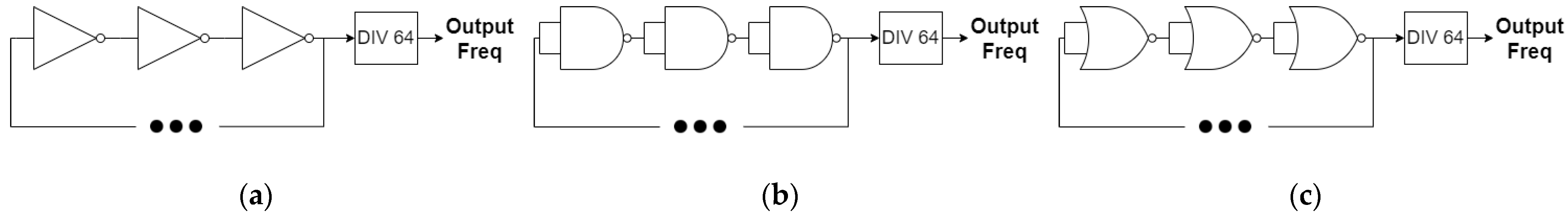
To evaluate TID effects, a 22-nm FD SOI test chip was designed and fabricated. Ring oscillators (ROs), flip-flop (FF) chains, and a static random access memory (SRAM) block were chosen as the testing vehicles for evaluating the technology’s susceptibility to TID effects; including both Co-60 and heavy ions irradiation sources [
12]. RO circuits can offer insights into gate delays due to changes in the frequency of the circuits, as well as changes in power consumption as dosage increases. The FF chains and the SRAM block can be used to offer a broad perspective on device functionality. A similar test chip with 28-nm FD SOI technology was also fabricated previously, and the results from that test chip will be used in this paper for comparison purposes between the two technologies [
9].
The organization of the rest of this paper is as follows. In
Section 2, details of the test circuits are introduced. In
Section 3, details of the test chip design and experimental setup are described. In
Section 4, the experimental results will be presented and discussed. Lastly, conclusions are drawn in
Section 5.
3. Test Chip Design
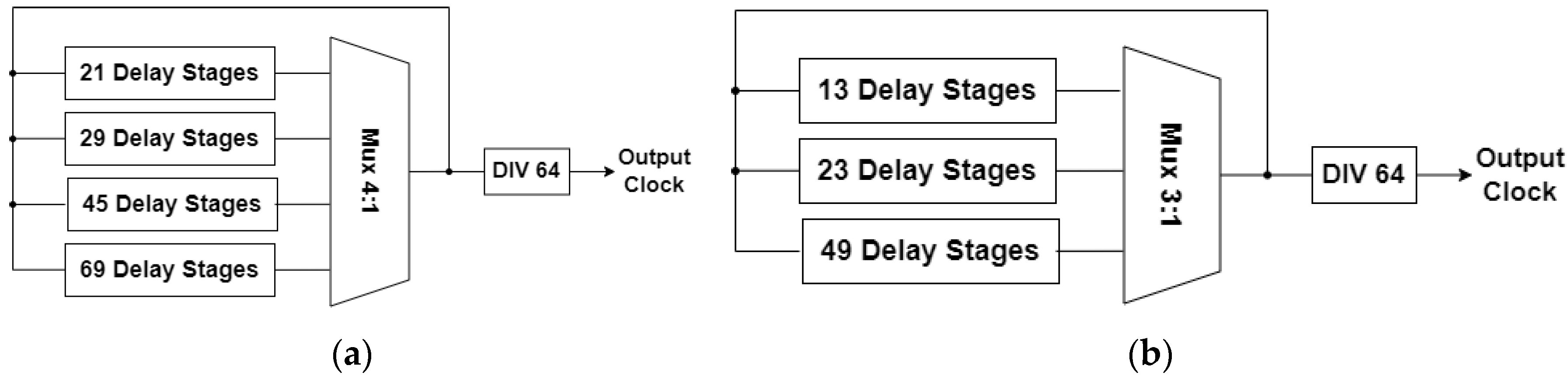
A test chip consisting of the three types of circuits previously discussed was developed and fabricated in a commercial 22-nm FD SOI technology, as shown in
Figure 5. All FF chains shared the same data input. The outputs of the SRAM block and FF chains were connected to the IO pads for external error detection, and the outputs of the RO circuits were connected to the IO pads for the frequency measurements. The nominal core logic supply voltage for this technology was 0.8 V, and the IO voltage was 1.8 V. Functional verification testing was carried out on the fabricated SRAM and FF chains with all 0s, 1s, and checker-board input patterns before irradiation.
A testing system consisting of power supplies, an FPGA board, and a microcontroller used during testing. The test chip was soldered onto a custom-made daughter board and was connected to the FPGA via a DIMM connection. During testing, the FFs, SRAM, and ROs were powered at their nominal voltage of 0.8 V. The FF chains were clocked at 1 MHz with the ‘all 0’ data input pattern, and current readings were taken from the power supplies every minute. The SRAM block was also clocked at 1 MHz, and a checker-board data pattern was used. At the beginning of testing, all addresses in the SRAM were written with the test data. Then, the content of the SRAM was continually read out to check if the data were still appropriately stored. If there was a mismatch in data, the system would record the event and attempt to repair the address with the correct test data, and the process would continue. If the address data could not be repaired, then that address location was considered non-functional and recorded.
During testing, the ROs were also powered at their nominal voltage of 0.8 V. The output pins of the ROs were connected to counters inside the FPGA and monitored the number of oscillations of each RO within a 0.1 s period. By knowing the number of oscillations for a given period, the frequency of each RO was able to be determined. During testing, all collected data on the FPGA were transferred to a microcontroller via a serial connection, where the data were logged and recorded so that testing personnel could evaluate the experimental data in real-time.
4. TID Experimental Results and Discussions
The TID experiments were performed by using a Gammacell 220 Co-60 chamber (
Figure 6) at the University of Saskatchewan, Saskatoon, SK, Canada. The Gammacell 220 chamber can provide an irradiation rate of 108.2 rad(Si) per minute. The total absorbed dose during the experiments was 1 Mrad.
The frequencies of the ROs were recorded during the TID testing and plotted in
Figure 7. It should be noted that the observed experimental data are a linear trend, so a first-order polynomial curve fitting was implemented to understand this trend better. It is interesting to note that the ROs with the same gate type experienced the same decreasing rate in their output frequency during testing. This can simply be attributed to the same gate delay degradation during TID testing.
The relative change in frequency was calculated from the ROs designed with inverters, NAND2, and NOR2 gates and listed in
Table 4. For the inverter-based RO, the relative decrease in frequency was the average of the drops in four different stage options; for the NAND2 and NOR2-based ROs, the average value of the drops in three different stage options was used to calculate the relative decrease in frequency. From the results, a trend emerged showing that ROs built using different gates were impacted by TID effects at differing rates.
Table 4 shows that the frequencies of the NAND2 ROs were least affected by the TID, whereas the NOR2 ROs were most affected. It is noted that the NAND2 gates have two NMOS transistors in series and two PMOS in parallel, whereas the NOR2 gates have two PMOS transistors in series and two NMOS in parallel. The sizing of the NMOS and PMOS network of the NAND2 and NOR2 gates used in the ROs was designed such that the rising and falling time were roughly equal. In general, the positive charge trapped in the BOX under the transistors due to TID irradiation results in a negative shift of the threshold voltage, which leads to an increased driving current of the NMOS transistor and reduced driving current for the PMOS transistors in the gates. Findings in [
2] show that the PMOS driving current is significantly reduced compared to the increase in the NMOS driving current in 28-nm FD SOI technology, which leads to the monotonic decrease in the frequency with the irradiation dose. The experimental results in this paper also show the same trends. The results of the NAND2 and NOR2 ROs further validate this since NOR2 has two PMOS transistors in series, which further degrades the delay of the gate, and hence reduces the frequency of the ROs.
TID testing with heavy ion irradiation was conducted at the Texas A&M University (TAMU) Cyclotron Institute. An irradiation rate of 60.9 rad(Si) per second was provided.
Figure 8 shows the change of the frequencies as the increase in the heavy ions TID exposure for the inverter-based RO (45 stages), NAND2-based RO (23 stages), and NOR2-based RO (23 stages). The results still show that the NOR2 RO has the largest frequency degradation, while the NAND2 RO has the least, which was demonstrated from the previous analysis. In addition, it can be observed that the degradation of the RO frequency from the Co-60 test is much more than the heavy ion test. Despite the use of the High-K dielectric gates in advanced technologies, which can help to reduce the radiation-induced voltage shift in the gate insulator, the radiation-induced charge in SOI buried oxides and shallow trench isolation oxide (STI) can cause degradation or failures as well [
19]. Electron-hole pairs are generated in the oxide layers when applying high-energy ionizing radiation, but most holes and electrons can immediately recombine. For high LET particles, such as heavy ions, they generate high-density charge pairs, making the initial recombination rate significantly large. The charge pair line density is relatively small for the low LET particles, such as Co-60, which reduces the initial recombination rate. Compared to the heavy ions, the Co-60 has a better ability and efficiency to create the trapped charges in oxide layers [
9], as reported in [
20,
21], respectively.
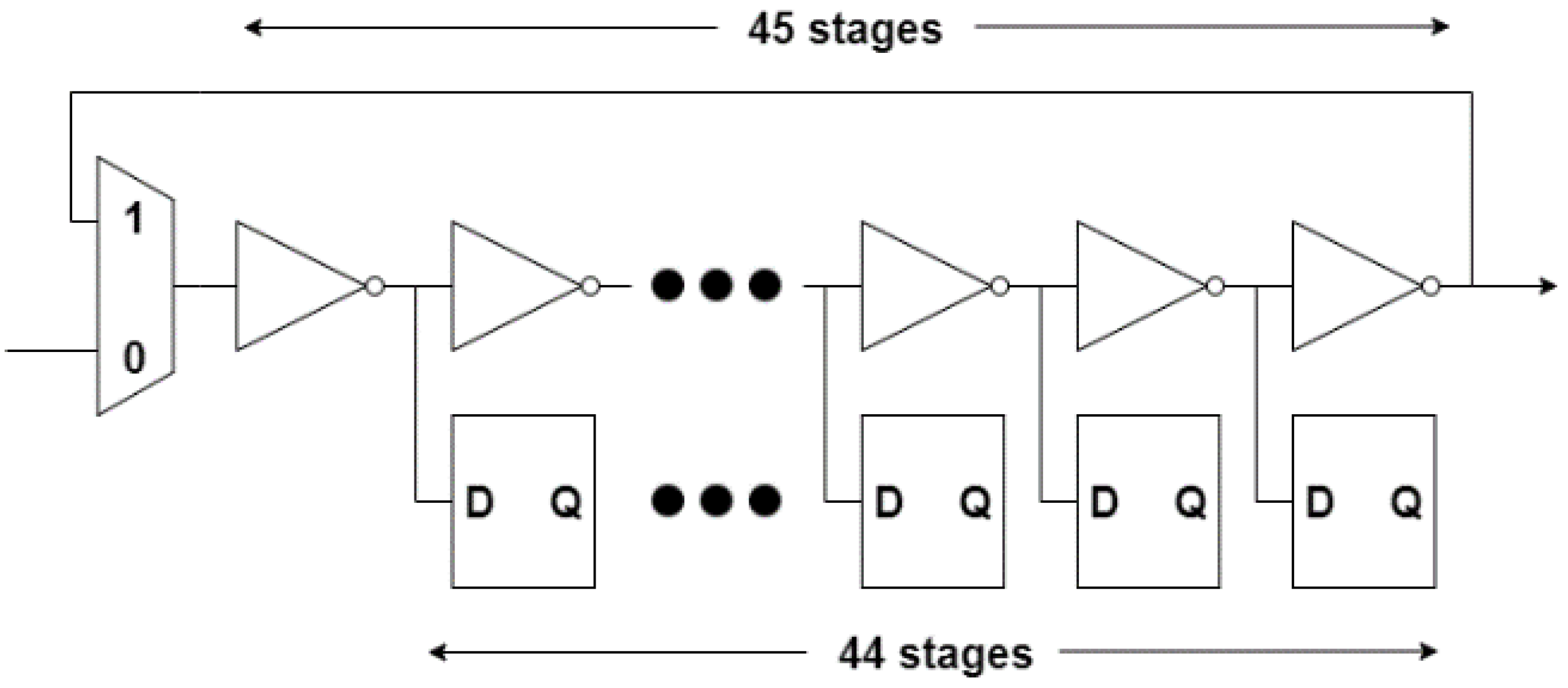
Another inverter-based RO in 28-nm technology was used for comparison. There are 45 stages in the 28-nm RO, and 44 of them are also used as delay stages contributing to other designs. A multiplexer was used to switch between these two modes, as shown in
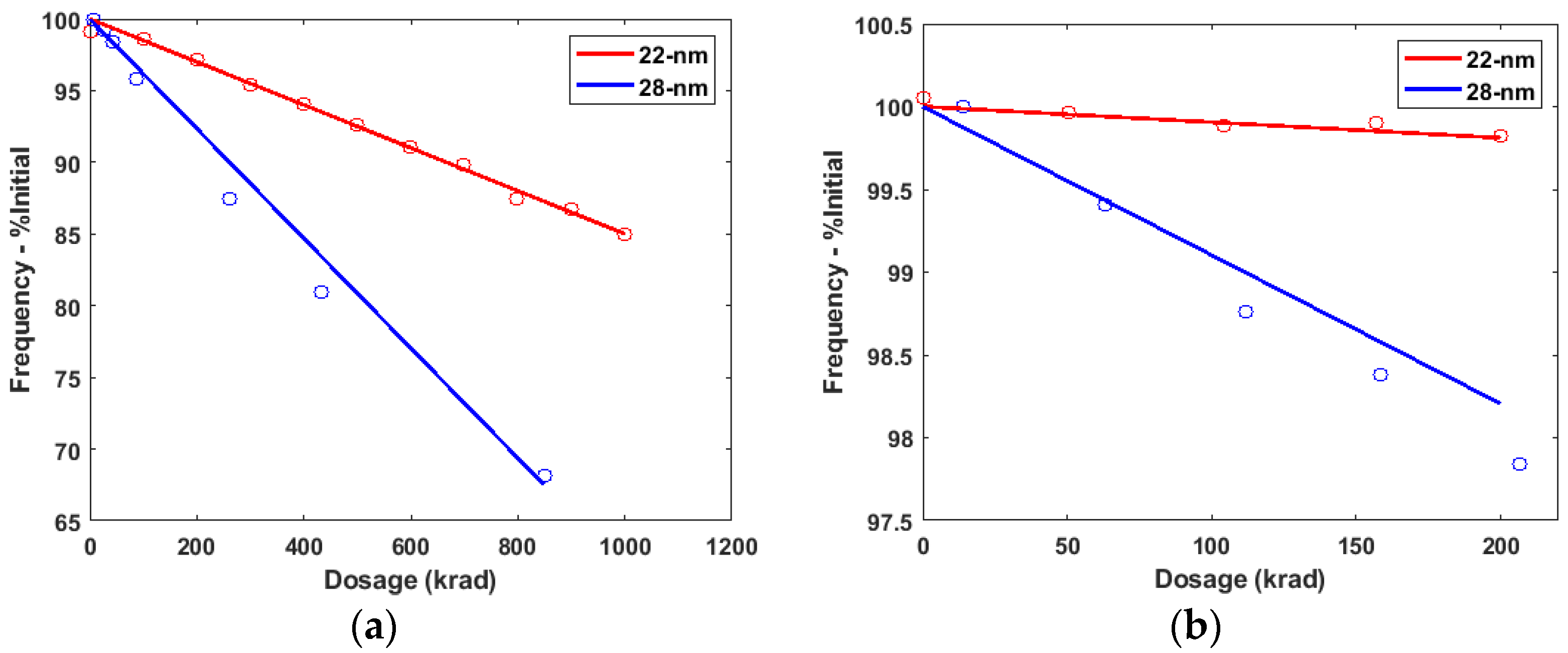
Figure 9. When the select input is high, the design will work as an RO. The 28-nm RO was also based on the conventional inverter without any layout optimizing techniques, which is the same as the 22-nm design, making these two designs fully comparable. The frequency versus total dose for two inverter-based ROs (45 stages and 69 stages, respectively) in the 28-nm and 22-nm FD SOI technologies are plotted in
Figure 10. These results show that during the Co-60 test at 850 krad(Si) of dosage, the 28-nm RO had a frequency decrease of over 30% from the initial, compared to the 14.5% decrease in 22-nm RO. During the heavy ion test, at 200 krad(Si) of dosage, the 28-nm RO had a frequency decrease of around 1.8% from the initial, compared to a less than 0.5% decrease in the 22-nm RO. These results show that the degradation in frequency for the 22-nm inverter-based RO has significantly improved. This indicates that the PMOS driving current is less affected by the TID effects for the 22-nm technology node, which could be due to manufacturing improvements. It is known that a thinner SiO
2 BOX layer can lead to a milder TID effect [
18,
22]. The thicknesses of the BOX and the SOI body of the 28-nm FD SOI technology are 25-nm and 7-nm [
23], and those are 20-nm and 6-nm in the 22-nm FD SOI technology node, respectively [
24]. The BOX of the 22-nm process is 25% thinner than that of the 28-nm process, so a less positive charge will be deposited in the BOX of the 22-nm process during irradiation. This will cause less interference with the threshold voltage of the 22-nm process, eventually leading to better resilience to TID effects.
Figure 11 shows the change in power supply current as the TID exposure increased for both 22-nm and 28-nm test circuits for Co-60 irradiation. Both of the plots are normalized. The current of 22-nm influenced by cumulative TID exposure is very similar to that of the 28-nm test. However, the current of the 22-nm test increased by approximately 18 times after 800 krad(Si) dosage compared to the initial starting current, while the 28-nm showed a 10 times increase. The increase in driving and leakage currents in the transistors can explain this increase in the current draw as the dose rate increases. These data show that TID effects are still prominent in the 22-nm FD SOI node. In addition, in the 22-nm technology node, the increase in the leakage current shows a linear trend from low doses to high doses.
The SRAM operated normally during testing until its functionality deteriorated at 325 krad(Si) of the total dosage. At this point, the number of recorded errors increased drastically, and every address showed a loss in functionality by 332 krad(Si) of the total dosage. A series of troubleshooting tests were performed to try and return functionality back to the SRAM block. These included resetting the test program, power cycling the SRAM, and clocking the SRAM at a slower rate of 100 kHz. None of these methods yielded any results, and the SRAM block was presumed dead. The FFs were still functional after the 1000 krad(Si) total absorbed dose, and no error was observed on any of the FF chains. In this case, it is believed that the SRAM storage cells themselves did not fail at 325 krad(Si), but instead, some part of the peripheral circuitry became damaged. For example, the internal operation of the SRAM block is controlled by a self-timing, asynchronous circuit, which could fail due to the increased delay, and this would explain why the entirety of the SRAM block failed at the same time instead of a more gradual loss in functionality. In this case, this timing issue caused by TID should be taken into account when designing the memory. For example, the self-timing circuit in the SRAM should be designed to be tolerant of the additional delay induced by the TID. Another method is to apply the back-gate voltage to the peripheral circuitry. When applying the back-gate voltage to circuits in the flipped well configuration, the drive current will be enhanced, and the delay will be reduced, which should effectively mitigate the TID effect in the peripheral circuitry.


 ,
, 


