
Nonvolatile Memories in Spiking Neural Network Architectures: Current and Emerging Trends


Abstract
:1. Introduction
- A complete overview of device physics, working, and drawbacks of the NVM devices.
- We discuss nonvolatile memory integration in hybrid CMOS and NVMs neuromorphic architectures with in-memory computing abilities, including large-scale and edge computing systems.
- We discuss relevant and up-to-date publications on SNN computing architectures with NVM devices.
- We provide a roadmap for the coming years, providing outlooks on the new applications in which NVMs are critical enablers.
2. Trends in Nonvolatile Memory-Based SNN Architectures
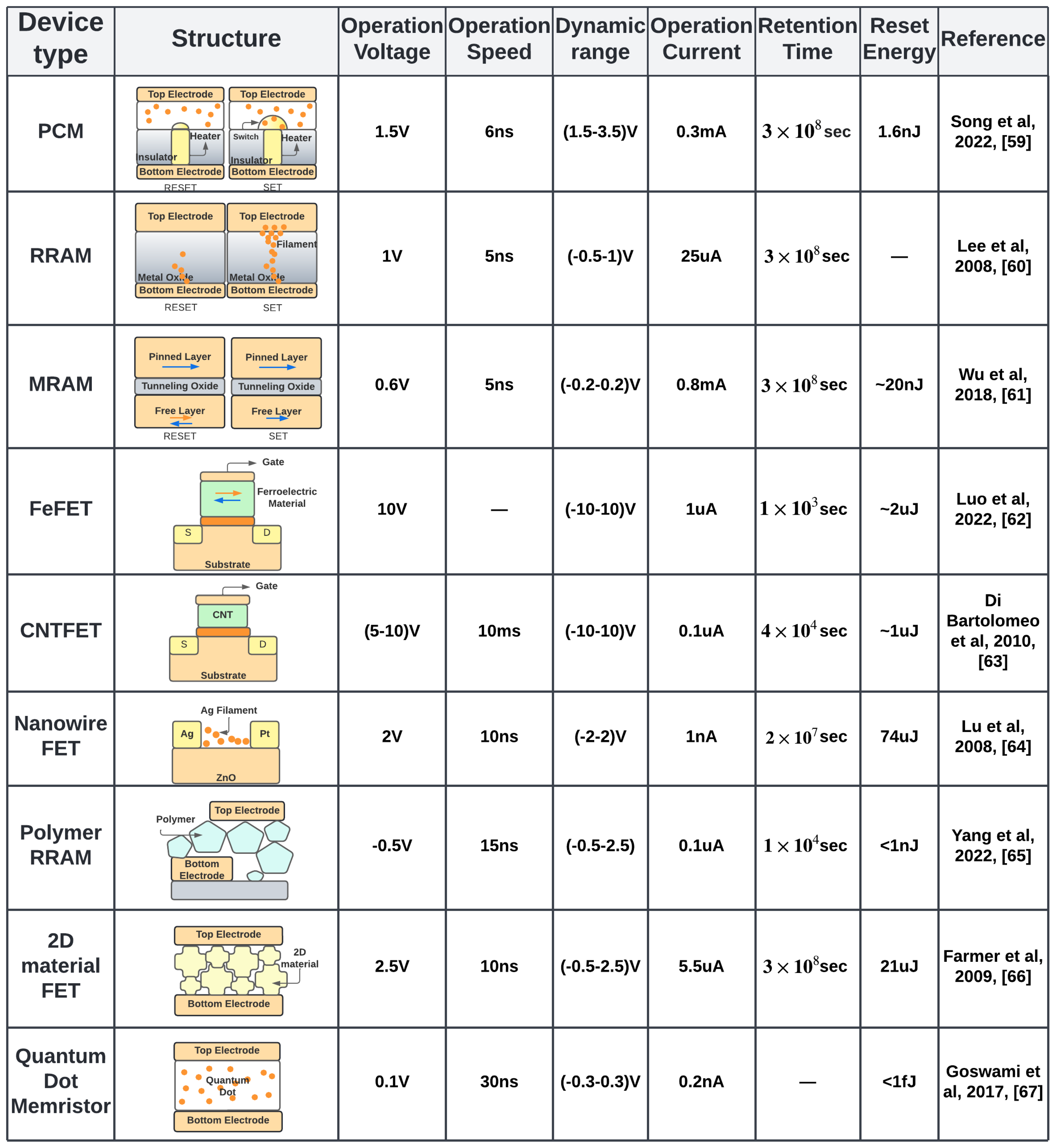
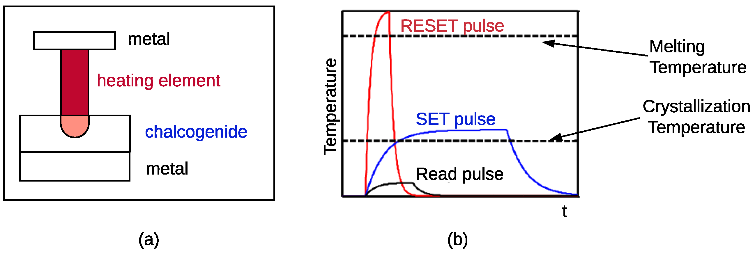
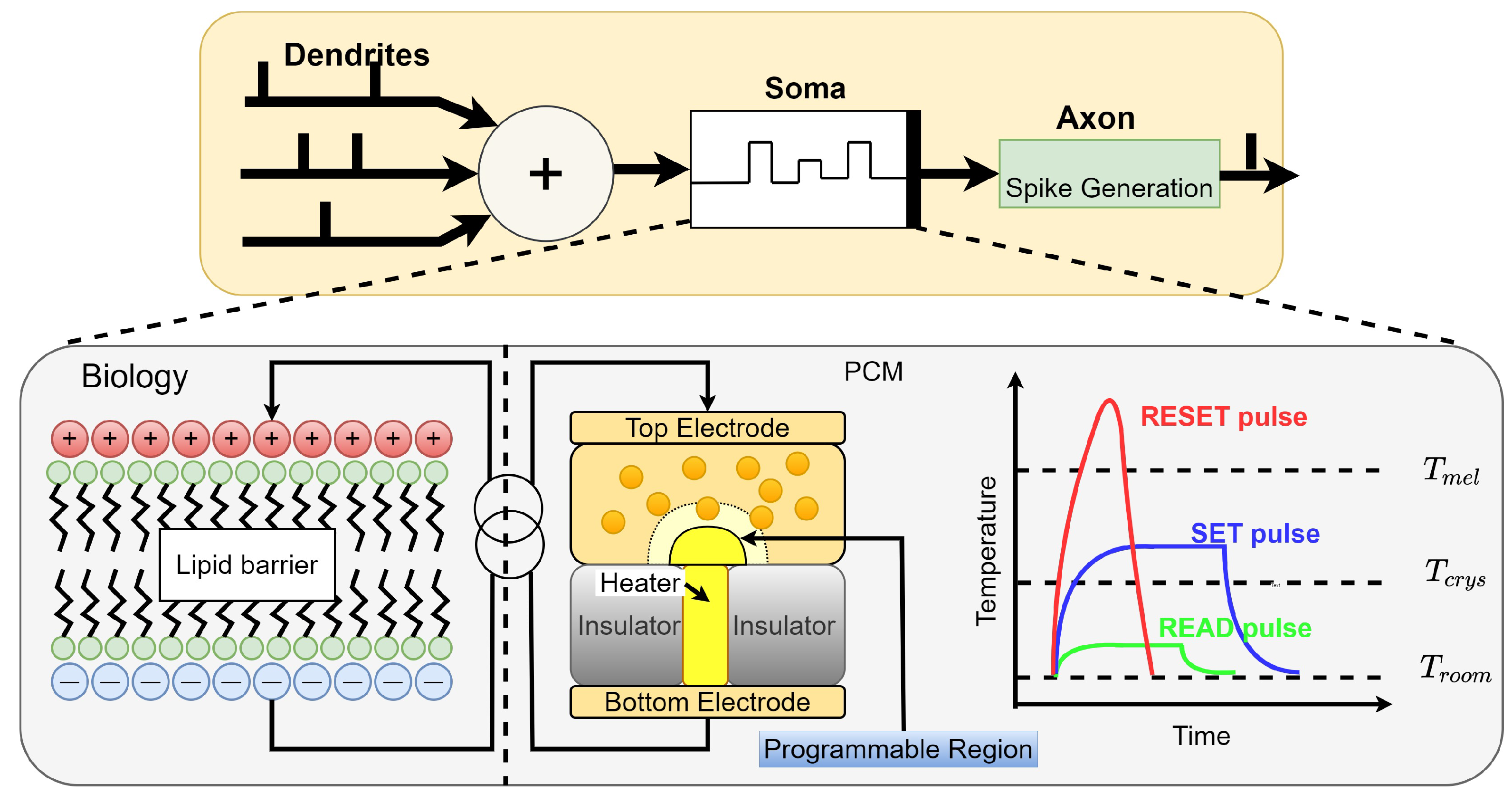
2.1. Phase-Change Memory
2.2. Resistive Ram
2.3. Magnetoresistive Ram
2.4. Ferroelectric Fet
2.5. Nanowires
3. Emerging Materials for NVM Devices
3.1. Polymer
3.2. 2D Materials
3.3. Quantum Dot
3.4. Carbon Nanotube
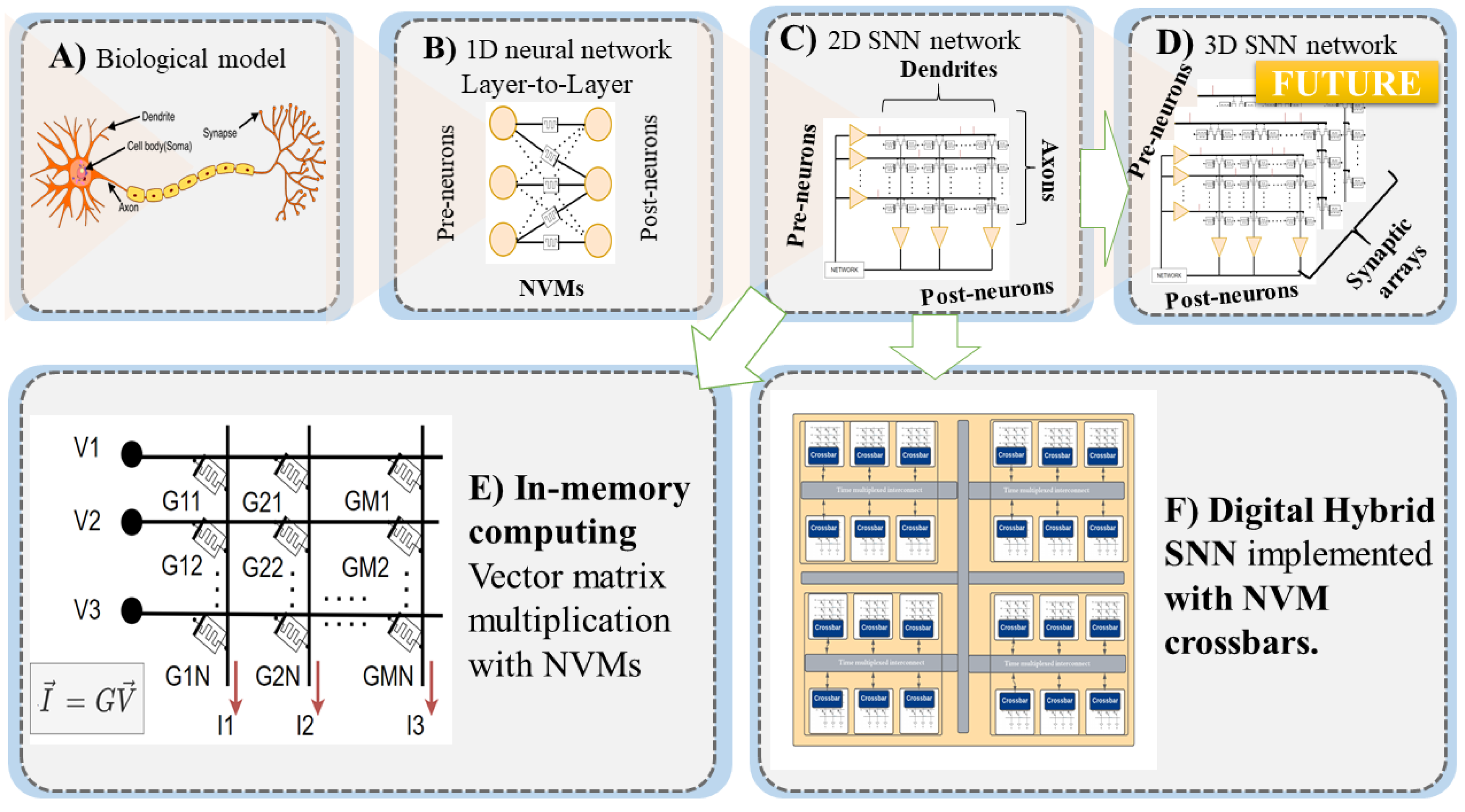
4. Large-Scale SNN Architectures with NVMs
5. SNN Edge Computing Architectures with NVMs
6. Discussion and Conclusions
Author Contributions
Funding
Conflicts of Interest
References
- Mead, C. Neuromorphic electronic systems. Proc. IEEE 1990, 78, 1629–1636. [Google Scholar] [CrossRef] [Green Version]
- Maass, W. Networks of spiking neurons: The third generation of neural network models. Neural Netw. 1997, 10, 1659–1671. [Google Scholar] [CrossRef]
- Sengupta, A.; Ye, Y.; Wang, R.; Liu, C.; Roy, K. Going deeper in spiking neural networks: VGG and residual architectures. Front. Neurosci. 2019, 13, 95. [Google Scholar] [CrossRef] [PubMed]
- Das, A.; Pradhapan, P.; Groenendaal, W.; Adiraju, P.; Rajan, R.; Catthoor, F.; Schaafsma, S.; Krichmar, J.; Dutt, N.; Van Hoof, C. Unsupervised heart-rate estimation in wearables with Liquid states and a probabilistic readout. Neural Netw. 2018, 99, 134–147. [Google Scholar] [CrossRef] [Green Version]
- Balaji, A.; Corradi, F.; Das, A.; Pande, S.; Schaafsma, S.; Catthoor, F. Power-accuracy trade-offs for heartbeat classification on neural networks hardware. J. Low Power Electron. 2018, 14, 508–519. [Google Scholar] [CrossRef] [Green Version]
- Hu, Y.; Tang, H.; Pan, G. Spiking Deep Residual Networks. IEEE Trans. Neural Netw. Learn. Syst. 2018, 1–6. Available online: https://ieeexplore.ieee.org/abstract/document/9597475 (accessed on 16 March 2022). [CrossRef]
- Bohte, S.M.; Kok, J.N.; La Poutré, J.A. SpikeProp: Backpropagation for networks of spiking neurons. In Proceedings of the European Symposium on Artificial Neural Networks, Bruges, Belgium, 26–28 April 2000. [Google Scholar]
- Yin, B.; Corradi, F.; Bohté, S.M. Accurate and efficient time-domain classification with adaptive spiking recurrent neural networks. Nat. Mach. Intell. 2021, 3, 905–913. [Google Scholar] [CrossRef]
- Perez-Nieves, N.; Goodman, D. Sparse spiking gradient descent. NeurIPS 2021, 34. Available online: https://proceedings.neurips.cc/paper/2021/hash/61f2585b0ebcf1f532c4d1ec9a7d51aa-Abstract.html (accessed on 16 March 2022).
- Davies, M. Benchmarks for progress in neuromorphic computing. Nat. Mach. Intell. 2019, 1, 386–388. [Google Scholar] [CrossRef]
- Das, A.; Catthoor, F.; Schaafsma, S. Heartbeat classification in wearables using multi-layer perceptron and time-frequency joint distribution of ECG. In Proceedings of the 2018 IEEE/ACM International Conference on Connected Health: Applications, Systems and Engineering Technologies, Washington, DC, USA, 26–28 September 2018. [Google Scholar]
- Corradi, F.; Pande, S.; Stuijt, J.; Qiao, N.; Schaafsma, S.; Indiveri, G.; Catthoor, F. ECG-based heartbeat classification in neuromorphic hardware. In Proceedings of the 2019 International Joint Conference on Neural Networks (IJCNN), Budapest, Hungary, 14–19 July 2019. [Google Scholar]
- Furber, S. Large-scale neuromorphic computing systems. J. Neural Eng. 2016, 13, 051001. [Google Scholar] [CrossRef]
- Schuman, C.D.; Potok, T.E.; Patton, R.M.; Birdwell, J.D.; Dean, M.E.; Rose, G.S.; Plank, J.S. A survey of neuromorphic computing and neural networks in hardware. arXiv 2017, arXiv:1705.06963. [Google Scholar]
- Marković, D.; Mizrahi, A.; Querlioz, D.; Grollier, J. Physics for neuromorphic computing. Nat. Rev. Phys. 2020, 2, 499–510. [Google Scholar] [CrossRef]
- Burr, G.W.; Shelby, R.M.; Sebastian, A.; Kim, S.; Kim, S.; Sidler, S.; Virwani, K.; Ishii, M.; Narayanan, P.; Fumarola, A.; et al. Neuromorphic computing using non-volatile memory. Adv. Phys. X 2017, 2, 89–124. [Google Scholar] [CrossRef]
- Esser, S.K.; Appuswamy, R.; Merolla, P.; Arthur, J.V.; Modha, D.S. Backpropagation for energy-efficient neuromorphic computing. NeurIPS 2015, 28. Available online: https://proceedings.neurips.cc/paper/2015/hash/10a5ab2db37feedfdeaab192ead4ac0e-Abstract.html (accessed on 16 March 2022).
- Indiveri, G.; Liu, S.C. Memory and information processing in neuromorphic systems. Proc. IEEE 2015, 103, 1379–1397. [Google Scholar] [CrossRef] [Green Version]
- Lin, C.K.; Wild, A.; Chinya, G.N.; Lin, T.H.; Davies, M.; Wang, H. Mapping Spiking Neural Networks onto a Manycore Neuromorphic Architecture. ACM SIGPLAN Notice 2018, 53, 78–89. [Google Scholar] [CrossRef]
- Das, A.; Wu, Y.; Huynh, K.; Dell’Anna, F.; Catthoor, F.; Schaafsma, S. Mapping of local and global synapses on spiking neuromorphic hardware. In Proceedings of the 2018 Design, Automation & Test in Europe Conference & Exhibition (DATE), Dresden, Germany, 19–23 March 2018. [Google Scholar]
- Ji, Y.; Zhang, Y.; Li, S.; Chi, P.; Jiang, C.; Qu, P.; Xie, Y.; Chen, W. NEUTRAMS: Neural network transformation and co-design under neuromorphic hardware constraints. In Proceedings of the 2016 49th Annual IEEE/ACM International Symposium on Microarchitecture (MICRO), Taipei, Taiwan, 15–19 October 2016. [Google Scholar]
- Balaji, A.; Das, A.; Wu, Y.; Huynh, K.; Dell’anna, F.G.; Indiveri, G.; Krichmar, J.L.; Dutt, N.D.; Schaafsma, S.; Catthoor, F. Mapping spiking neural networks to neuromorphic hardware. IEEE Trans. Very Large Scale Integr. Syst. 2020, 28, 76–86. [Google Scholar] [CrossRef]
- Song, S.; Chong, H.; Balaji, A.; Das, A.; Shackleford, J.; Kandasamy, N. DFSynthesizer: Dataflow-based synthesis of spiking neural networks to neuromorphic hardware. ACM Trans. Embed. Comput. Syst. 2021. [Google Scholar] [CrossRef]
- Titirsha, T.; Song, S.; Balaji, A.; Das, A. On the Role of System Software in Energy Management of Neuromorphic Computing. In Proceedings of the 18th ACM International Conference on Computing Frontiers, Virtual, 11–13 May 2021; pp. 124–132. [Google Scholar] [CrossRef]
- Paul, A.; Tajin, M.A.S.; Das, A.; Mongan, W.; Dandekar, K. Energy-Efficient Respiratory Anomaly Detection in Premature Newborn Infants. Electronics 2022, 11, 682. [Google Scholar] [CrossRef]
- Balaji, A.; Adiraju, P.; Kashyap, H.J.; Das, A.; Krichmar, J.L.; Dutt, N.D.; Catthoor, F. PyCARL: A PyNN interface for hardware-software co-simulation of spiking neural network. arXiv 2020, arXiv:2003.09696. [Google Scholar]
- Curzel, S.; Agostini, N.B.; Song, S.; Dagli, I.; Limaye, A.; Tan, C.; Minutoli, M.; Castellana, V.G.; Amatya, V.; Manzano, J.; et al. Automated Generation of Integrated Digital and Spiking Neuromorphic Machine Learning Accelerators. In Proceedings of the 2021 IEEE/ACM International Conference On Computer Aided Design (ICCAD), Munich, Germany, 1–4 November 2021. [Google Scholar]
- Song, S.; Mirtinti, L.V.; Das, A.; Kandasamy, N. A Design Flow for Mapping Spiking Neural Networks to Many-Core Neuromorphic Hardware. In Proceedings of the 2021 IEEE/ACM International Conference On Computer Aided Design (ICCAD), Munich, Germany, 1–4 November 2021. [Google Scholar]
- Huynh, P.K.; Varshika, M.L.; Paul, A.; Isik, M.; Balaji, A.; Das, A. Implementing Spiking Neural Networks on Neuromorphic Architectures: A Review. arXiv 2022, arXiv:2202.08897. [Google Scholar]
- Varshika, M.L.; Balaji, A.; Corradi, F.; Das, A.; Stuijt, J.; Catthoor, F. Design of Many-Core Big Little μBrains for Energy-Efficient Embedded Neuromorphic Computing. arXiv 2021, arXiv:arXiv:2111.11838. [Google Scholar]
- Balaji, A.; Song, S.; Titirsha, T.; Das, A.; Krichmar, J.; Dutt, N.; Shackleford, J.; Kandasamy, N.; Catthoor, F. NeuroXplorer 1.0: An Extensible Framework for Architectural Exploration with Spiking Neural Networks. In Proceedings of the International Conference on Neuromorphic Systems 2021, Knoxville, TN, USA, 27–29 July 2021. [Google Scholar]
- Furber, S.; Galluppi, F.; Temple, S.; Plana, L.A. The SpiNNaker project. Proc. IEEE 2014, 102, 652–665. [Google Scholar] [CrossRef]
- Debole, M.V.; Taba, B.; Amir, A.; Akopyan, F.; Andreopoulos, A.; Risk, W.P.; Kusnitz, J.; Otero, C.O.; Nayak, T.K.; Appuswamy, R.; et al. TrueNorth: Accelerating from zero to 64 million neurons in 10 years. Computer 2019, 52, 20–29. [Google Scholar] [CrossRef]
- Davies, M.; Srinivasa, N.; Lin, T.H.; Chinya, G.; Cao, Y.; Choday, S.H.; Dimou, G.; Joshi, P.; Imam, N.; Jain, S.; et al. Loihi: A neuromorphic manycore processor with on-chip learning. IEEE Micro 2018, 38, 82–99. [Google Scholar] [CrossRef]
- Stuijt, J.; Sifalakis, M.; Yousefzadeh, A.; Corradi, F. μBrain: An Event-Driven and Fully Synthesizable Architecture for Spiking Neural Networks. Front. Neurosci. 2021, 15, 538. [Google Scholar] [CrossRef]
- Frenkel, C.; Lefebvre, M.; Legat, J.D.; Bol, D. A 0.086-mm2 12.7-pJ/SOP 64k-synapse 256-neuron online-learning digital spiking neuromorphic processor in 28-nm CMOS. IEEE Trans. Biomed. Circuits Syst. 2019, 13, 145–158. [Google Scholar]
- Benjamin, B.; Gao, P.; McQuinn, E.; Choudhary, S.; Chandrasekaran, A.R.; Bussat, J.M.; Alvarez-Icaza, R.; Arthur, J.V.; Merolla, P.A.; Boahen, K. Neurogrid: A mixed-analog-digital multichip system for large-scale neural simulations. Proc. IEEE 2014, 102, 699–716. [Google Scholar] [CrossRef]
- Schemmel, J.; Grübl, A.; Hartmann, S.; Kononov, A.; Mayr, C.; Meier, K.; Millner, S.; Partzsch, J.; Schiefer, S.; Scholze, S.; et al. Live demonstration: A scaled-down version of the brainscales wafer-scale neuromorphic system. In Proceedings of the 2012 IEEE international symposium on circuits and systems (ISCAS), Seoul, Korea, 20–23 May 2012. [Google Scholar]
- Shi, L.; Pei, J.; Deng, N.; Wang, D.; Deng, L.; Wang, Y.; Zhang, Y.; Chen, F.; Zhao, M.; Song, S.; et al. Development of a neuromorphic computing system. In Proceedings of the 2015 IEEE International Electron Devices Meeting (IEDM), Washington, DC, USA, 7–9 December 2015. [Google Scholar]
- Chi, P.; Li, S.; Xu, C.; Zhang, T.; Zhao, J.; Liu, Y.; Wang, Y.; Xie, Y. PRIME: A Novel Processing-in-Memory Architecture for Neural Network Computation in ReRAM-Based Main Memory. ACM Sigarch Comput. Archit. News 2016, 44, 27–39. [Google Scholar] [CrossRef]
- Moradi, S.; Qiao, N.; Stefanini, F.; Indiveri, G. A scalable multicore architecture with heterogeneous memory structures for dynamic neuromorphic asynchronous processors (DYNAPs). IEEE Trans. Biomed. Circuits Syst. 2017, 12, 106–122. [Google Scholar] [CrossRef] [Green Version]
- Xia, Q.; Yang, J.J. Memristive crossbar arrays for brain-inspired computing. Nat. Mater. 2019, 18, 309–323. [Google Scholar] [CrossRef] [PubMed]
- Chakraborty, I.; Jaiswal, A.; Saha, A.; Gupta, S.; Roy, K. Pathways to efficient neuromorphic computing with non-volatile memory technologies. Appl. Phys. Rev. 2020, 7, 021308. [Google Scholar] [CrossRef]
- Islam, R.; Li, H.; Chen, P.Y.; Wan, W.; Chen, H.Y.; Gao, B.; Wu, H.; Yu, S.; Saraswat, K.; Wong, H.P. Device and materials requirements for neuromorphic computing. J. Phys. Appl. Phys. 2019, 52, 113001. [Google Scholar] [CrossRef]
- Chen, A. A review of emerging non-volatile memory (NVM) technologies and applications. Solid-State Electron. 2016, 125, 25–38. [Google Scholar] [CrossRef]
- Liu, D.; Yu, H.; Chai, Y. Low-power computing with neuromorphic engineering. Adv. Intell. Syst. 2021, 3, 2000150. [Google Scholar] [CrossRef]
- Strenz, R. Review and outlook on embedded nvm technologies–from evolution to revolution. In Proceedings of the 2020 IEEE International Memory Workshop (IMW), Dresden, Germany, 17–20 May 2020. [Google Scholar]
- Burr, G.W.; Sebastian, A.; Vianello, E.; Waser, R.; Parkin, S. Emerging materials in neuromorphic computing: Guest editorial. APL Mater. 2020, 8, 010401. [Google Scholar] [CrossRef]
- Mehonic, A.; Sebastian, A.; Rajendran, B.; Simeone, O.; Vasilaki, E.; Kenyon, A.J. Memristors—From In-Memory Computing, Deep Learning Acceleration, and Spiking Neural Networks to the Future of Neuromorphic and Bio-Inspired Computing. Adv. Intell. Syst. 2020, 2, 2000085. [Google Scholar] [CrossRef]
- Lee, B.; Ipek, E.; Mutlu, O.; Burger, D. Architecting Phase Change Memory As a Scalable DRAM Alternative. In Proceedings of the 36th annual international symposium on Computer architecture, Austin, TX, USA, 20–24 June 2009. [Google Scholar]
- Mutlu, O. Memory scaling: A systems architecture perspective. In Proceedings of the 2013 5th IEEE International Memory Workshop, Monterey, CA, USA, 26–29 May 2013. [Google Scholar]
- Song, S.; Das, A.; Kandasamy, N. Exploiting Inter- and Intra-Memory Asymmetries for Data Mapping in Hybrid Tiered-Memories. In Proceedings of the 2020 ACM SIGPLAN International Symposium on Memory Management, London, UK, 16 June 2020. [Google Scholar]
- Eisenman, A.; Gardner, D.; AbdelRahman, I.; Axboe, J.; Dong, S.; Hazelwood, K.; Petersen, C.; Cidon, A.; Katti, S. Reducing DRAM footprint with NVM in Facebook. In Proceedings of the Thirteenth EuroSys Conference, Porto, Portugal, 23–26 April 2018. [Google Scholar]
- Burr, G.W.; Kurdi, B.N.; Scott, J.C.; Lam, C.H.; Gopalakrishnan, K.; Shenoy, R.S. Overview of candidate device technologies for storage-class memory. IBM J. Res. Dev. 2008, 52, 449–464. [Google Scholar] [CrossRef] [Green Version]
- Kuzum, D.; Yu, S.; Wong, H.P. Synaptic electronics: Materials, devices and applications. Nanotechnology 2013, 24, 382001. [Google Scholar] [CrossRef]
- Giulioni, M.; Corradi, F.; Dante, V.; Del Giudice, P. Real time unsupervised learning of visual stimuli in neuromorphic VLSI systems. Sci. Rep. 2015, 5, 14730. [Google Scholar] [CrossRef] [Green Version]
- Burr, G.W.; Shelby, R.M.; Sidler, S.; Di Nolfo, C.; Jang, J.; Boybat, I.; Shenoy, R.S.; Narayanan, P.; Virwani, K.; Giacometti, E.U.; et al. Experimental demonstration and tolerancing of a large-scale neural network (165,000 synapses) using phase-change memory as the synaptic weight element. IEEE Trans. Electron Devices 2015, 62, 3498–3507. [Google Scholar] [CrossRef]
- Yan, Y.; Wu, X.; Chen, Q.; Wang, X.; Li, E.; Liu, Y.; Chen, H.; Guo, T. An intrinsically healing artificial neuromorphic device. J. Mater. Chem. C 2020, 8, 6869–6876. [Google Scholar] [CrossRef]
- Song, Z.; Wang, R.; Xue, Y.; Song, S. The “gene” of reversible phase transformation of phase change materials: Octahedral motif. Nano Res. 2022, 15, 765–772. [Google Scholar] [CrossRef]
- Lee, H.; Chen, P.; Wu, T.; Chen, Y.; Wang, C.; Tzeng, P.; Lin, C.; Chen, F.; Lien, C.; Tsai, M.J. Low power and high speed bipolar switching with a thin reactive Ti buffer layer in robust HfO2 based RRAM. In Proceedings of the 2008 IEEE International Electron Devices Meeting, San Francisco, CA, USA, 15–17 December 2008. [Google Scholar]
- Wu, L.; Taouil, M.; Rao, S.; Marinissen, E.J.; Hamdioui, S. Electrical modeling of STT-MRAM defects. In Proceedings of the 2018 IEEE International Test Conference (ITC), Phoenix, AZ, USA, 29 October–1 November 2018. [Google Scholar]
- Luo, Z.D.; Zhang, S.; Liu, Y.; Zhang, D.; Gan, X.; Seidel, J.; Liu, Y.; Han, G.; Alexe, M.; Hao, Y. Dual-Ferroelectric-Coupling-Engineered Two-Dimensional Transistors for Multifunctional In-Memory Computing. ACS Nano 2022, 16, 3362–3372. [Google Scholar] [CrossRef]
- Di Bartolomeo, A.; Rinzan, M.; Boyd, A.K.; Yang, Y.; Guadagno, L.; Giubileo, F.; Barbara, P. Electrical properties and memory effects of field-effect transistors from networks of single-and double-walled carbon nanotubes. Nanotechnology 2010, 21, 115204. [Google Scholar] [CrossRef]
- Lu, W.; Xie, P.; Lieber, C.M. Nanowire transistor performance limits and applications. IEEE Trans. Electron Devices 2008, 55, 2859–2876. [Google Scholar] [CrossRef]
- Yang, J.M.; Choi, E.S.; Kim, S.Y.; Kim, J.H.; Park, J.H.; Park, N.G. Perovskite-related (CH 3 NH 3) 3 Sb 2 Br 9 for forming-free memristor and low-energy-consuming neuromorphic computing. Nanoscale 2019, 11, 6453–6461. [Google Scholar] [CrossRef]
- Farmer, D.B.; Chiu, H.Y.; Lin, Y.M.; Jenkins, K.A.; Xia, F.; Avouris, P. Utilization of a buffered dielectric to achieve high field-effect carrier mobility in graphene transistors. Nano Lett. 2009, 9, 4474–4478. [Google Scholar] [CrossRef] [Green Version]
- Goswami, S.; Matula, A.J.; Rath, S.P.; Hedström, S.; Saha, S.; Annamalai, M.; Sengupta, D.; Patra, A.; Ghosh, S.; Jani, H.; et al. Robust resistive memory devices using solution-processable metal-coordinated azo aromatics. Nat. Mater. 2017, 16, 1216–1224. [Google Scholar] [CrossRef]
- Wong, H.S.P.; Raoux, S.; Kim, S.; Liang, J.; Reifenberg, J.P.; Rajendran, B.; Asheghi, M.; Goodson, K.E. Phase change memory. Proc. IEEE 2010, 98, 2201–2227. [Google Scholar] [CrossRef]
- Burr, G.W.; Breitwisch, M.J.; Franceschini, M.; Garetto, D.; Gopalakrishnan, K.; Jackson, B.; Kurdi, B.; Lam, C.; Lastras, L.A.; Padilla, A.; et al. Phase change memory technology. J. Vac. Sci. Technol. Nanotechnol. Microelectron. Mater. Process. Meas. Phenom. 2010, 28, 223–262. [Google Scholar] [CrossRef] [Green Version]
- Bez, R. Chalcogenide PCM: A memory technology for next decade. In Proceedings of the 2009 IEEE International Electron Devices Meeting (IEDM), Baltimore, MD, USA, 7–9 December 2009. [Google Scholar]
- Jones, R.O. Phase change memory materials: Rationalizing the dominance of Ge/Sb/Te alloys. Phys. Rev. B 2020, 101, 024103. [Google Scholar] [CrossRef]
- Raoux, S.; Xiong, F.; Wuttig, M.; Pop, E. Phase change materials and phase change memory. MRS Bull. 2014, 39, 703–710. [Google Scholar] [CrossRef] [Green Version]
- Zahoor, F.; Azni Zulkifli, T.Z.; Khanday, F.A. Resistive random access memory (RRAM): An overview of materials, switching mechanism, performance, multilevel cell (MLC) storage, modeling, and applications. Nanoscale Res. Lett. 2020, emph15, 1–26. [Google Scholar] [CrossRef] [PubMed]
- Papandreou, N.; Pantazi, A.; Sebastian, A.; Breitwisch, M.; Lam, C.; Pozidis, H.; Eleftheriou, E. Multilevel phase-change memory. In Proceedings of the 2010 17th IEEE International Conference on Electronics, Circuits and Systems, Athens, Greece, 12–15 December 2010. [Google Scholar]
- Stanisavljevic, M.; Pozidis, H.; Athmanathan, A.; Papandreou, N.; Mittelholzer, T.; Eleftheriou, E. Demonstration of reliable triple-level-cell (TLC) phase-change memory. In Proceedings of the 2016 IEEE 8th International Memory Workshop (IMW), Paris, France, 15–18 May 2016. [Google Scholar]
- Sebastian, A.; Le Gallo, M.; Burr, G.W.; Kim, S.; BrightSky, M.; Eleftheriou, E. Tutorial: Brain-inspired computing using phase-change memory devices. J. Appl. Phys. 2018, 124, 111101. [Google Scholar] [CrossRef] [Green Version]
- Kuzum, D.; Jeyasingh, R.G.; Lee, B.; Wong, H.S.P. Nanoelectronic programmable synapses based on phase change materials for brain-inspired computing. Nano Lett. 2012, 12, 2179–2186. [Google Scholar] [CrossRef] [PubMed]
- Caporale, N.; Dan, Y. Spike timing–dependent plasticity: A Hebbian learning rule. Annu. Rev. Neurosci. 2008, 31, 25–46. [Google Scholar] [CrossRef] [Green Version]
- Bichler, O.; Suri, M.; Querlioz, D.; Vuillaume, D.; DeSalvo, B.; Gamrat, C. Visual pattern extraction using energy-efficient 2-PCM synapse neuromorphic architecture. IEEE Trans. Electron Devices 2012, 59, 2206–2214. [Google Scholar] [CrossRef]
- Kuzum, D.; Jeyasingh, R.G.; Wong, H.S.P. Energy efficient programming of nanoelectronic synaptic devices for large-scale implementation of associative and temporal sequence learning. In Proceedings of the 2011 International Electron Devices Meeting, Washington, DC, USA, 5–7 December 2011. [Google Scholar]
- Li, Y.; Zhong, Y.; Xu, L.; Zhang, J.; Xu, X.; Sun, H.; Miao, X. Ultrafast synaptic events in a chalcogenide memristor. Sci. Rep. 2013, 3, 1619. [Google Scholar] [CrossRef] [Green Version]
- Titirsha, T.; Song, S.; Das, A.; Krichmar, J.; Dutt, N.; Kandasamy, N.; Catthoor, F. Endurance-Aware Mapping of Spiking Neural Networks to Neuromorphic Hardware. IEEE Trans. Parallele Distrib. Syst. 2021, 33, 288–301. [Google Scholar] [CrossRef]
- Titirsha, T.; Das, A. Thermal-Aware Compilation of Spiking Neural Networks to Neuromorphic Hardware. arXiv 2020, arXiv:2010.04773. [Google Scholar]
- Eryilmaz, S.B.; Kuzum, D.; Jeyasingh, R.G.; Kim, S.; BrightSky, M.; Lam, C.; Wong, H.S.P. Experimental demonstration of array-level learning with phase change synaptic devices. In Proceedings of the 2013 IEEE International Electron Devices Meeting, Washington, DC, USA, 9–11 December 2013. [Google Scholar]
- Ambrogio, S.; Narayanan, P.; Tsai, H.; Shelby, R.M.; Boybat, I.; Di Nolfo, C.; Sidler, S.; Giordano, M.; Bodini, M.; Farinha, N.C.; et al. Equivalent-accuracy accelerated neural-network training using analogue memory. Nature 2018, 558, 60–67. [Google Scholar] [CrossRef] [PubMed]
- Song, S.; Das, A. A case for lifetime reliability-aware neuromorphic computing. arXiv 2020, arXiv:2007.02210. [Google Scholar]
- Kundu, S.; Basu, K.; Sadi, M.; Titirsha, T.; Song, S.; Das, A.; Guin, U. Special Session: Reliability Analysis for ML/AI Hardware. arXiv 2021, arXiv:2103.12166. [Google Scholar]
- Balaji, A.; Song, S.; Das, A.; Dutt, N.; Krichmar, J.; Kandasamy, N.; Catthoor, F. A framework to explore workload-specific performance and lifetime trade-offs in neuromorphic computing. IEEE Comput. Archit. Lett. 2019, 18, 149–152. [Google Scholar] [CrossRef] [Green Version]
- Song, S.; Das, A.; Kandasamy, N. Improving dependability of neuromorphic computing with non-volatile memory. arXiv 2020, arXiv:2006.05868. [Google Scholar]
- Song, S.; Hanamshet, J.; Balaji, A.; Das, A.; Krichmar, J.; Dutt, N.; Kandasamy, N.; Catthoor, F. Dynamic reliability management in neuromorphic computing. ACM J. Emerg. Technol. Comput. Syst. 2021, 17, 1–27. [Google Scholar] [CrossRef]
- Kim, I.; Cho, S.; Im, D.; Cho, E.; Kim, D.; Oh, G.; Ahn, D.; Park, S.; Nam, S.; Moon, J.; et al. High performance PRAM cell scalable to sub-20nm technology with below 4F2 cell size, extendable to DRAM applications. In Proceedings of the 2010 Symposium on VLSI Technology, Honolulu, HI, USA, 15–17 June 2010. [Google Scholar]
- Wang, L.; Yang, C.H.; Wen, J. Physical principles and current status of emerging non-volatile solid state memories. Electron. Mater. Lett. 2015, 11, 505–543. [Google Scholar] [CrossRef]
- Burr, G.; Virwani, K.; Shenoy, R.; Fraczak, G.; Rettner, C.; Padilla, A.; King, R.; Nguyen, K.; Bowers, A.; Jurich, M.; et al. Recovery dynamics and fast (sub-50ns) read operation with access devices for 3D crosspoint memory based on mixed-ionic-electronic-conduction (MIEC). In Proceedings of the 2013 Symposium on VLSI Technology, Kyoto, Japan, 11–13 June 2013. [Google Scholar]
- Pirovano, A.; Lacaita, A.L.; Pellizzer, F.; Kostylev, S.A.; Benvenuti, A.; Bez, R. Low-field amorphous state resistance and threshold voltage drift in chalcogenide materials. IEEE Trans. Electron Devices 2004, 51, 714–719. [Google Scholar] [CrossRef]
- Dirisaglik, F.; Bakan, G.; Jurado, Z.; Muneer, S.; Akbulut, M.; Rarey, J.; Sullivan, L.; Wennberg, M.; King, A.; Zhang, L.; et al. High speed, high temperature electrical characterization of phase change materials: Metastable phases, crystallization dynamics, and resistance drift. Nanoscale 2015, 7, 16625–16630. [Google Scholar] [CrossRef]
- Titirsha, T.; Das, A. Reliability-Performance Trade-offs in Neuromorphic Computing. In Proceedings of the 2020 11th International Green and Sustainable Computing Workshops (IGSC), Pullman, WA, USA, 19–22 October 2020. [Google Scholar]
- Hickmott, T. Low-frequency negative resistance in thin anodic oxide films. J. Appl. Phys. 1962, 33, 2669–2682. [Google Scholar] [CrossRef]
- Akinaga, H.; Shima, H. Resistive random access memory (ReRAM) based on metal oxides. Proc. IEEE 2010, 98, 2237–2251. [Google Scholar] [CrossRef]
- Burkitt, A.N. A review of the integrate-and-fire neuron model: I. Homogeneous synaptic input. Biol. Cybern. 2006, 95, 1–19. [Google Scholar] [CrossRef]
- Prezioso, M.; Merrikh Bayat, F.; Hoskins, B.; Likharev, K.; Strukov, D. Self-adaptive spike-time-dependent plasticity of metal-oxide memristors. Sci. Rep. 2016, 6, 21331. [Google Scholar] [CrossRef] [PubMed]
- Yu, S.; Wu, Y.; Jeyasingh, R.; Kuzum, D.; Wong, H.S.P. An electronic synapse device based on metal oxide resistive switching memory for neuromorphic computation. IEEE Trans. Electron Devices 2011, 58, 2729–2737. [Google Scholar] [CrossRef]
- Valentian, A.; Rummens, F.; Vianello, E.; Mesquida, T.; de Boissac, C.L.M.; Bichler, O.; Reita, C. Fully integrated spiking neural network with analog neurons and RRAM synapses. In Proceedings of the 2019 IEEE International Electron Devices Meeting (IEDM), San Francisco, CA, USA, 7–11 December 2019. [Google Scholar]
- Hansen, M.; Ziegler, M.; Kolberg, L.; Soni, R.; Dirkmann, S.; Mussenbrock, T.; Kohlstedt, H. A double barrier memristive device. Sci. Rep. 2015, 5, 13753. [Google Scholar] [CrossRef] [Green Version]
- Yang, R.; Terabe, K.; Yao, Y.; Tsuruoka, T.; Hasegawa, T.; Gimzewski, J.K.; Aono, M. Synaptic plasticity and memory functions achieved in a WO3-x-based nanoionics device by using the principle of atomic switch operation. Nanotechnology 2013, 24, 384003. [Google Scholar] [CrossRef]
- Goux, L.; Valov, I. Electrochemical processes and device improvement in conductive bridge RAM cells. Phys. Status Solidi 2016, 213, 274–288. [Google Scholar] [CrossRef]
- Fackenthal, R.; Kitagawa, M.; Otsuka, W.; Prall, K.; Mills, D.; Tsutsui, K.; Javanifard, J.; Tedrow, K.; Tsushima, T.; Shibahara, Y.; et al. 19.7 A 16 Gb ReRAM with 200 MB/s write and 1 GB/s read in 27 nm technology. In Proceedings of the 2014 IEEE International Solid-State Circuits Conference Digest of Technical Papers (ISSCC), San Francisco, CA, USA, 9–13 February 2014. [Google Scholar]
- Wijesinghe, P.; Ankit, A.; Sengupta, A.; Roy, K. An all-memristor deep spiking neural computing system: A step toward realizing the low-power stochastic brain. IEEE Trans. Emerg. Top. Comput. Intell. 2018, 2, 345–358. [Google Scholar] [CrossRef]
- Shim, W.; Luo, Y.; Seo, J.s.; Yu, S. Impact of read disturb on multilevel RRAM based inference engine: Experiments and model prediction. In Proceedings of the 2020 IEEE International Reliability Physics Symposium (IRPS), Dallas, TX, USA, 28 April–30 May 2020. [Google Scholar]
- Song, S.; Titirsha, T.; Das, A. Improving Inference Lifetime of Neuromorphic Systems via Intelligent Synapse Mapping. In Proceedings of the 2021 IEEE 32nd International Conference on Application-Specific Systems, Architectures and Processors (ASAP), Virtual, 7–9 July 2021. [Google Scholar]
- Paul, A.; Das, A. Design Technology Co-Optimization for Neuromorphic Computing. In Proceedings of the 2021 12th International Green and Sustainable Computing Conference (IGSC), Pullman, WA, USA, 18–21 October 2021. [Google Scholar]
- Paul, A.; Song, S.; Titirsha, T.; Das, A. On the Mitigation of Read Disturbances in Neuromorphic Inference Hardware. arXiv 2022, arXiv:2201.11527. [Google Scholar] [CrossRef]
- Mallik, A.; Garbin, D.; Fantini, A.; Rodopoulos, D.; Degraeve, R.; Stuijt, J.; Das, A.; Schaafsma, S.; Debacker, P.; Donadio, G.; et al. Design-technology co-optimization for OxRRAM-based synaptic processing unit. In Proceedings of the 2017 Symposium on VLSI Technology, Kyoto, Japan, 5–8 June 2017. [Google Scholar]
- Valov, I.; Waser, R.; Jameson, J.R.; Kozicki, M.N. Electrochemical metallization memories—Fundamentals, applications, prospects. Nanotechnology 2011, 22, 254003. [Google Scholar] [CrossRef] [PubMed]
- Menzel, S.; Böttger, U.; Wimmer, M.; Salinga, M. Physics of the switching kinetics in resistive memories. Adv. Funct. Mater. 2015, 25, 6306–6325. [Google Scholar] [CrossRef]
- Cüppers, F.; Menzel, S.; Bengel, C.; Hardtdegen, A.; Von Witzleben, M.; Böttger, U.; Waser, R.; Hoffmann-Eifert, S. Exploiting the switching dynamics of HfO2-based ReRAM devices for reliable analog memristive behavior. APL Mater. 2019, 7, 091105. [Google Scholar] [CrossRef] [Green Version]
- Zhu, J.G. Magnetoresistive random access memory: The path to competitiveness and scalability. Proc. IEEE 2008, 96, 1786–1798. [Google Scholar]
- Zhao, W.; Belhaire, E.; Chappert, C.; Jacquet, F.; Mazoyer, P. New non-volatile logic based on spin-MTJ. Phys. Status Solidi 2008, 205, 1373–1377. [Google Scholar] [CrossRef]
- Khvalkovskiy, A.; Apalkov, D.; Watts, S.; Chepulskii, R.; Beach, R.; Ong, A.; Tang, X.; Driskill-Smith, A.; Butler, W.; Visscher, P.; et al. Basic principles of STT-MRAM cell operation in memory arrays. J. Phys. Appl. Phys. 2013, 46, 074001. [Google Scholar] [CrossRef]
- Apalkov, D.; Khvalkovskiy, A.; Watts, S.; Nikitin, V.; Tang, X.; Lottis, D.; Moon, K.; Luo, X.; Chen, E.; Ong, A.; et al. Spin-transfer torque magnetic random access memory (STT-MRAM). ACM J. Emerg. Technol. Comput. Syst. 2013, 9, 1–35. [Google Scholar] [CrossRef]
- Rzeszut, P.; Chęciński, J.; Brzozowski, I.; Ziętek, S.; Skowroński, W.; Stobiecki, T. Multi-state MRAM cells for hardware neuromorphic computing. arXiv 2021, arXiv:2102.03415. [Google Scholar] [CrossRef]
- Endoh, T.; Honjo, H.; Nishioka, K.; Ikeda, S. Recent progresses in STT-MRAM and SOT-MRAM for next generation MRAM. In Proceedings of the 2020 IEEE Symposium on VLSI Technology, Honolulu, HI, USA, 16–19 June 2020. [Google Scholar]
- Sengupta, A.; Al Azim, Z.; Fong, X.; Roy, K. Spin-orbit torque induced spike-timing dependent plasticity. Appl. Phys. Lett. 2015, 106, 093704. [Google Scholar] [CrossRef] [Green Version]
- Ostwal, V.; Zand, R.; DeMara, R.; Appenzeller, J. A novel compound synapse using probabilistic spin–orbit-torque switching for MTJ-based deep neural networks. JXCDC 2019, 5, 182–187. [Google Scholar] [CrossRef]
- Sharad, M.; Augustine, C.; Panagopoulos, G.; Roy, K. Spin-based neuron model with domain-wall magnets as synapse. IEEE J. Explor. Solid-State Comput. Devices Circuits 2012, 11, 843–853. [Google Scholar] [CrossRef] [Green Version]
- Sengupta, A.; Shim, Y.; Roy, K. Proposal for an all-spin artificial neural network: Emulating neural and synaptic functionalities through domain wall motion in ferromagnets. IEEE Trans. Biomed. Circuits Syst. 2016, 10, 1152–1160. [Google Scholar] [CrossRef] [PubMed]
- Christensen, D.; Dittmann, R.; Linares-Barranco, B.; Sebastian, A.; Gallo, M.; Redaelli, A.; Slesazeck, S.; Mikolajick, T.; Spiga, S.; Menzel, S.; et al. Roadmap on Neuromorphic Computing and Engineering. arXiv 2021, arXiv:2105.05956. [Google Scholar]
- Xu, Y. Ferroelectric Materials and Their Applications; Elsevier: Amsterdam, The Netherlands, 2013. [Google Scholar]
- Aziz, A.; Breyer, E.T.; Chen, A.; Chen, X.; Datta, S.; Gupta, S.K.; Hoffmann, M.; Hu, X.S.; Ionescu, A.; Jerry, M.; et al. Computing with ferroelectric FETs: Devices, models, systems, and applications. In Proceedings of the 2018 Design, Automation & Test in Europe Conference & Exhibition (DATE), Dresden, Germany, 19–23 March 2018. [Google Scholar]
- Banerjee, W. Challenges and applications of emerging nonvolatile memory devices. Electronics 2020, 9, 1029. [Google Scholar] [CrossRef]
- Mulaosmanovic, H.; Mikolajick, T.; Slesazeck, S. Accumulative polarization reversal in nanoscale ferroelectric transistors. ACS Appl. Mater. Interfaces 2018, 10, 23997–24002. [Google Scholar] [CrossRef]
- Mulaosmanovic, H.; Ocker, J.; Müller, S.; Noack, M.; Müller, J.; Polakowski, P.; Mikolajick, T.; Slesazeck, S. Novel ferroelectric FET based synapse for neuromorphic systems. In Proceedings of the 2017 Symposium on VLSI Technology, Kyoto, Japan, 5–8 June 2017. [Google Scholar]
- Kaneko, Y.; Nishitani, Y.; Ueda, M.; Tsujimura, A. Neural network based on a three-terminal ferroelectric memristor to enable on-chip pattern recognition. In Proceedings of the 2013 Symposium on VLSI Technology, Kyoto, Japan, 11–13 June 2013. [Google Scholar]
- Chen, X.; Yin, X.; Niemier, M.; Hu, X.S. Design and optimization of FeFET-based crossbars for binary convolution neural networks. In Proceedings of the 2018 Design, Automation & Test in Europe Conference & Exhibition (DATE), Dresden, Germany, 19–23 March 2018. [Google Scholar]
- Milano, G.; Pedretti, G.; Fretto, M.; Boarino, L.; Benfenati, F.; Ielmini, D.; Valov, I.; Ricciardi, C. Brain-inspired structural plasticity through reweighting and rewiring in multi-terminal self-organizing memristive nanowire networks. Adv. Intell. Syst. 2020, 2, 2000096. [Google Scholar] [CrossRef]
- Li, Q.; Diaz-Alvarez, A.; Iguchi, R.; Hochstetter, J.; Loeffler, A.; Zhu, R.; Shingaya, Y.; Kuncic, Z.; Uchida, K.i.; Nakayama, T. Dynamic electrical pathway tuning in neuromorphic nanowire networks. Adv. Funct. Mater. 2020, 30, 2003679. [Google Scholar] [CrossRef]
- Breitenstein, O. Nondestructive local analysis of current–voltage characteristics of solar cells by lock-in thermography. Sol. Energy Mater. Sol. Cells 2011, 95, 2933–2936. [Google Scholar] [CrossRef]
- Zhao, Y.Y.; Sun, W.J.; Wang, J.; He, J.H.; Li, H.; Xu, Q.F.; Li, N.J.; Chen, D.Y.; Lu, J.M. All-inorganic ionic polymer-based memristor for high-performance and flexible artificial synapse. Adv. Funct. Mater. 2020, 30, 2004245. [Google Scholar] [CrossRef]
- Fuller, E.J.; Keene, S.T.; Melianas, A.; Wang, Z.; Agarwal, S.; Li, Y.; Tuchman, Y.; James, C.D.; Marinella, M.J.; Yang, J.J.; et al. Parallel programming of an ionic floating-gate memory array for scalable neuromorphic computing. Science 2019, 364, 570–574. [Google Scholar] [CrossRef]
- Haigh, S.J.; Gholinia, A.; Jalil, R.; Romani, S.; Britnell, L.; Elias, D.C.; Novoselov, K.S.; Ponomarenko, L.A.; Geim, A.K.; Gorbachev, R. Cross-sectional imaging of individual layers and buried interfaces of graphene-based heterostructures and superlattices. Nat. Mater. 2012, 11, 764–767. [Google Scholar] [CrossRef] [PubMed] [Green Version]
- Cao, G.; Meng, P.; Chen, J.; Liu, H.; Bian, R.; Zhu, C.; Liu, F.; Liu, Z. 2D material based synaptic devices for neuromorphic computing. Adv. Funct. Mater. 2021, 31, 2005443. [Google Scholar] [CrossRef]
- Shi, Y.; Liang, X.; Yuan, B.; Chen, V.; Li, H.; Hui, F.; Yu, Z.; Yuan, F.; Pop, E.; Wong, H.S.P.; et al. Electronic synapses made of layered two-dimensional materials. Nat. Electron. 2018, 1, 458–465. [Google Scholar] [CrossRef]
- Wang, M.; Cai, S.; Pan, C.; Wang, C.; Lian, X.; Zhuo, Y.; Xu, K.; Cao, T.; Pan, X.; Wang, B.; et al. Robust memristors based on layered two-dimensional materials. Nat. Electron. 2018, 1, 130–136. [Google Scholar] [CrossRef] [Green Version]
- Xu, R.; Jang, H.; Lee, M.H.; Amanov, D.; Cho, Y.; Kim, H.; Park, S.; Shin, H.J.; Ham, D. Vertical MoS2 double-layer memristor with electrochemical metallization as an atomic-scale synapse with switching thresholds approaching 100 mV. Nano Lett. 2019, 19, 2411–2417. [Google Scholar] [CrossRef]
- Zhuang, P.; Ma, W.; Liu, J.; Cai, W.; Lin, W. Progressive RESET induced by Joule heating in hBN RRAMs. Appl. Phys. Lett. 2021, 118, 143101. [Google Scholar] [CrossRef]
- Chen, Y.; Zhou, Y.; Zhuge, F.; Tian, B.; Yan, M.; Li, Y.; He, Y.; Miao, X.S. Graphene–ferroelectric transistors as complementary synapses for supervised learning in spiking neural network. 2D Mater. Appl. 2019, 3, 1–9. [Google Scholar] [CrossRef]
- Zhu, X.; Li, D.; Liang, X.; Lu, W.D. Ionic modulation and ionic coupling effects in MoS2 devices for neuromorphic computing. Nat. Mater. 2019, 18, 141–148. [Google Scholar] [CrossRef]
- Yang, Y.; Chen, B.; Lu, W.D. Memristive physically evolving networks enabling the emulation of heterosynaptic plasticity. Adv. Mater. 2015, 27, 7720–7727. [Google Scholar] [CrossRef]
- Liao, Q.; Wang, Y.; Lv, Z.; Xiong, Z.; Chen, J.; Wang, G.P.; Han, S.T.; Zhou, Y. Electronic synapses mimicked in bilayer organic-inorganic heterojunction based memristor. Org. Electron. 2021, 90, 106062. [Google Scholar] [CrossRef]
- Sangwan, V.K.; Hersam, M.C. Neuromorphic nanoelectronic materials. Nat. Nanotechnol. 2020, 15, 517–528. [Google Scholar] [CrossRef] [PubMed]
- Lv, Z.; Wang, Y.; Chen, J.; Wang, J.; Zhou, Y.; Han, S.T. Semiconductor quantum dots for memories and neuromorphic computing systems. Chem. Rev. 2020, 120, 3941–4006. [Google Scholar] [CrossRef] [PubMed]
- Qi, M.; Zhang, X.; Yang, L.; Wang, Z.; Xu, H.; Liu, W.; Zhao, X.; Liu, Y. Intensity-modulated LED achieved through integrating p-GaN/n-ZnO heterojunction with multilevel RRAM. Appl. Phys. Lett. 2018, 113, 223503. [Google Scholar] [CrossRef]
- Roychowdhury, V.; Janes, D.; Bandyopadhyay, S.; Wang, X. Collective computational activity in self-assembled arrays of quantum dots: A novel neuromorphic architecture for nanoelectronics. IEEE Trans. Electron Devices 1996, 43, 1688–1699. [Google Scholar] [CrossRef]
- Feldmann, J.; Youngblood, N.; Wright, C.D.; Bhaskaran, H.; Pernice, W.H. All-optical spiking neurosynaptic networks with self-learning capabilities. Nature 2019, 569, 208–214. [Google Scholar] [CrossRef] [Green Version]
- Kim, S.; Yoon, J.; Kim, H.D.; Choi, S.J. Carbon nanotube synaptic transistor network for pattern recognition. Appl. Mater. Interfaces 2015, 7, 25479–25486. [Google Scholar] [CrossRef]
- Ananthanarayanan, R.; Esser, S.K.; Simon, H.D.; Modha, D.S. The cat is out of the bag: Cortical simulations with 109 neurons, 1013 synapses. In Proceedings of the Conference on High Performance Computing Networking, Storage and Analysis, Portland, OR, USA, 14–20 November 2009. [Google Scholar]
- Catthoor, F.; Mitra, S.; Das, A.; Schaafsma, S. Very large-scale neuromorphic systems for biological signal processing. In CMOS Circuits for Biological Sensing and Processing; Springer: Cham, Switzerland, 2018. [Google Scholar]
- Wang, I.T.; Lin, Y.C.; Wang, Y.F.; Hsu, C.W.; Hou, T.H. 3D synaptic architecture with ultralow sub-10 fJ energy per spike for neuromorphic computation. In Proceedings of the 2014 IEEE International Electron Devices Meeting, San Francisco, CA, USA, 15–17 December 2014. [Google Scholar]
- Shulaker, M.M.; Hills, G.; Park, R.S.; Howe, R.T.; Saraswat, K.; Wong, H.S.P.; Mitra, S. Three-dimensional integration of nanotechnologies for computing and data storage on a single chip. Nature 2017, 547, 74–78. [Google Scholar] [CrossRef]
- Song, S.; Balaji, A.; Das, A.; Kandasamy, N.; Shackleford, J. Compiling spiking neural networks to neuromorphic hardware. In Proceedings of the The 21st ACM SIGPLAN/SIGBED Conference on Languages, Compilers, and Tools for Embedded Systems, London, UK, 16 June 2020. [Google Scholar]
- Moro, F.; Esmanhotto, E.; Hirtzlin, T.; Castellani, N.; Trabelsi, A.; Dalgaty, T.; Molas, G.; Andrieu, F.; Brivio, S.; Spiga, S.; et al. Hardware calibrated learning to compensate heterogeneity in analog RRAM-based Spiking Neural Networks. arXiv 2022, arXiv:2202.05094. [Google Scholar]
- Luo, Q.; Xu, X.; Liu, H.; Lv, H.; Gong, T.; Long, S.; Liu, Q.; Sun, H.; Banerjee, W.; Li, L.; et al. Cu BEOL compatible selector with high selectivity (>107), extremely low off-current (pA) and high endurance (>1010). In Proceedings of the 2015 IEEE International Electron Devices Meeting (IEDM), Washington, DC, USA, 7–9 December 2015. [Google Scholar]
- Esmanhotto, E.; Brunet, L.; Castellani, N.; Bonnet, D.; Dalgaty, T.; Grenouillet, L.; Ly, D.; Cagli, C.; Vizioz, C.; Allouti, N.; et al. High-density 3D monolithically integrated multiple 1T1R multi-level-cell for neural networks. In Proceedings of the 2020 IEEE International Electron Devices Meeting (IEDM), San Francisco, CA, USA, 12–18 December 2020. [Google Scholar]
- Bourzac, K. Has Intel created a universal memory technology? [news]. IEEE Spectr. 2017, 54, 9–10. [Google Scholar] [CrossRef]
- Yang, H.; Hao, X.; Wang, Z.; Malmhall, R.; Gan, H.; Satoh, K.; Zhang, J.; Jung, D.H.; Wang, X.; Zhou, Y.; et al. Threshold switching selector and 1S1R integration development for 3D cross-point STT-MRAM. In Proceedings of the 2017 IEEE International Electron Devices Meeting (IEDM), San Francisco, CA, USA, 2–6 December 2017. [Google Scholar]
- Choi, Y.; Oh, S.; Qian, C.; Park, J.H.; Cho, J.H. Vertical organic synapse expandable to 3D crossbar array. Nat. Commun. 2020, 11, 1–9. [Google Scholar] [CrossRef]
- Alibart, F.; Pleutin, S.; Guérin, D.; Novembre, C.; Lenfant, S.; Lmimouni, K.; Gamrat, C.; Vuillaume, D. An organic nanoparticle transistor behaving as a biological spiking synapse. Adv. Funct. Mater. 2010, 20, 330–337. [Google Scholar] [CrossRef] [Green Version]
- Kim, S.; Choi, B.; Lim, M.; Yoon, J.; Lee, J.; Kim, H.D.; Choi, S.J. Pattern recognition using carbon nanotube synaptic transistors with an adjustable weight update protocol. ACS Nano 2017, 11, 2814–2822. [Google Scholar] [CrossRef] [PubMed]
- Shi, Y.; Ananthakrishnan, A.; Oh, S.; Liu, X.; Hota, G.; Cauwenberghs, G.; Kuzum, D. A Neuromorphic Brain Interface Based on RRAM Crossbar Arrays for High Throughput Real-Time Spike Sorting. IEEE Trans. Electron Devices 2022, 69, 2137–2144. [Google Scholar] [CrossRef]
- Song, S.; Balaji, A.; Das, A.; Kandasamy, N. Design-Technology Co-Optimization for NVM-based Neuromorphic Processing Elements. ACM Trans. Embed. Comput. Syst. 2022. [Google Scholar] [CrossRef]
- Oh, S.; Shi, Y.; Liu, X.; Song, J.; Kuzum, D. Drift-enhanced unsupervised learning of handwritten digits in spiking neural network with PCM synapses. IEEE Electron Device Lett. 2018, 39, 1768–1771. [Google Scholar] [CrossRef]
- Nomura, A.; Ito, M.; Okazaki, A.; Ishii, M.; Kim, S.; Okazawa, J.; Hosokawa, K.; Haensch, W. Analysis of effect of weight variation on SNN chip with PCM-refresh method. Neural Process. Lett. 2021, 53, 1741–1751. [Google Scholar] [CrossRef]
- Wang, Y.; Wu, D.; Wang, Y.; Hu, X.; Ma, Z.; Feng, J.; Xie, Y. A Low-Cost Hardware-Friendly Spiking Neural Network Based on Binary Mram Synapses, Accelerated Using In-Memory Computing. Electronics 2021, 10, 2441. [Google Scholar] [CrossRef]
- Jang, Y.; Kang, G.; Kim, T.; Seo, Y.; Lee, K.J.; Park, B.G.; Park, J. Stochastic SOT device based SNN architecture for On-chip Unsupervised STDP Learning. IEEE Trans. Comput. 2021. [Google Scholar] [CrossRef]
- Fang, Y.; Wang, Z.; Gomez, J.; Datta, S.; Khan, A.I.; Raychowdhury, A. A swarm optimization solver based on ferroelectric spiking neural networks. Front. Neurosci. 2019, 855. [Google Scholar] [CrossRef] [Green Version]
- Chang, M.F.; Sheu, S.S.; Lin, K.F.; Wu, C.W.; Kuo, C.C.; Chiu, P.F.; Yang, Y.S.; Chen, Y.S.; Lee, H.Y.; Lien, C.H.; et al. A high-speed 7.2-ns read-write random access 4-Mb embedded resistive RAM (ReRAM) macro using process-variation-tolerant current-mode read schemes. IEEE J. Solid-State Circuits 2012, 48, 878–891. [Google Scholar] [CrossRef]
- Kozicki, M.N.; Barnaby, H.J. Conductive bridging random access memory—Materials, devices and applications. Semicond. Sci. Technol. 2016, 31, 113001. [Google Scholar] [CrossRef]
- Gargini, P. Roadmap evolution: From NTRS to ITRS, from ITRS 2.0 to IRDS. In Proceedings of the Berkeley Symposium on Energy Efficient Electronic Systems & Steep Transistors Workshop (E3S), Berkeley, CA, USA, 19–20 October 2017. [Google Scholar]
- Truong, S.N. Single crossbar array of memristors with bipolar inputs for neuromorphic image recognition. IEEE Access 2020, 8, 69327–69332. [Google Scholar] [CrossRef]
- Kim, Y.; Panda, P. Visual explanations from spiking neural networks using inter-spike intervals. Sci. Rep. 2021, 11, 19037. [Google Scholar] [CrossRef] [PubMed]
- Park, S.; Kim, S.; Na, B.; Yoon, S. T2FSNN: Deep spiking neural networks with time-to-first-spike coding. In Proceedings of the 2020 57th ACM/IEEE Design Automation Conference (DAC), San Francisco, CA, USA, 20–24 July 2020. [Google Scholar]
- Lagorce, X.; Orchard, G.; Galluppi, F.; Shi, B.E.; Benosman, R.B. Hots: A hierarchy of event-based time-surfaces for pattern recognition. IEEE Trans. Pattern Anal. Mach. Intell. 2016, 39, 1346–1359. [Google Scholar] [CrossRef] [PubMed]
- Papistas, I.A.; Cosemans, S.; Rooseleer, B.; Doevenspeck, J.; Na, M.H.; Mallik, A.; Debacker, P.; Verkest, D. A 22 nm, 1540 TOP/s/W, 12.1 TOP/s/mm 2 in-memory analog matrix-vector-multiplier for DNN acceleration. In Proceedings of the 2021 IEEE Custom Integrated Circuits Conference (CICC), Austin, TX, USA, 25–30 April 2021. [Google Scholar]
- Ueyoshi, K.; Papistas, I.A.; Houshmand, P.; Sarda, G.M.; Jain, V.; Shi, M.; Zheng, Q.; Giraldo, S.; Vrancx, P.; Doevenspeck, J.; et al. DIANA: An End-to-End Energy-Efficient Digital and ANAlog Hybrid Neural Network SoC. In Proceedings of the 2022 IEEE International Solid-State Circuits Conference (ISSCC), San Francisco, CA, USA, 20–26 February 2022. [Google Scholar]


| Read Latency | Write Latency | Write Endurance | |
|---|---|---|---|
| PCM | ≈12 ns [129] | ≈100 ns [129] | ≈109 [129] |
| RRAM | ≈10 ns [175] | ≈10 ns [175] | ≈1012 [129] |
| CBRAM | ≈30 ns [176] | ≈15 ns–1 μs [176] | ≈108 [176] |
| MRAM | ≈2.5 ns [177] | ≈7.1 ns [177] | ≈1012 [177] |
| FeFET | ≈40 ns [129] | ≈65 ns [129] | ≈1014 [129] |
| CNTFET | ≈100 ns [126] | ≈100 ns [126] | ≈107 [126] |
Publisher’s Note: MDPI stays neutral with regard to jurisdictional claims in published maps and institutional affiliations. |
© 2022 by the authors. Licensee MDPI, Basel, Switzerland. This article is an open access article distributed under the terms and conditions of the Creative Commons Attribution (CC BY) license (https://creativecommons.org/licenses/by/4.0/).
Share and Cite
Varshika, M.L.; Corradi, F.; Das, A. Nonvolatile Memories in Spiking Neural Network Architectures: Current and Emerging Trends. Electronics 2022, 11, 1610. https://doi.org/10.3390/electronics11101610
Varshika ML, Corradi F, Das A. Nonvolatile Memories in Spiking Neural Network Architectures: Current and Emerging Trends. Electronics. 2022; 11(10):1610. https://doi.org/10.3390/electronics11101610
Chicago/Turabian StyleVarshika, M. Lakshmi, Federico Corradi, and Anup Das. 2022. "Nonvolatile Memories in Spiking Neural Network Architectures: Current and Emerging Trends" Electronics 11, no. 10: 1610. https://doi.org/10.3390/electronics11101610
APA StyleVarshika, M. L., Corradi, F., & Das, A. (2022). Nonvolatile Memories in Spiking Neural Network Architectures: Current and Emerging Trends. Electronics, 11(10), 1610. https://doi.org/10.3390/electronics11101610