Abstract
This paper proposes a hybrid converter to supply power from solar power source to load. Since power is generated by solar power, which depends on the intensity of solar power, the power generated by the solar power does not keep at a constant power. Therefore, the proposed system needs a battery to balance power between solar power and load. When the proposed one uses the battery to balance powers, the proposed circuit requires a charger and discharger. To simplify the proposed converter, a buck-boost converter and flyback converter can be combined to implement the battery charging and discharging functions. With this approach, the proposed converter can be operated with zero-voltage switching (ZVS) at turn-on transition to reduce switching loss of switch when the proposed one is operated in the discharging mode. In addition, the proposed hybrid converter has several merits, which are less component counts, lighter weight, smaller size and higher conversion efficiency. As compared with the conventional counterparts with hard-switching circuit, the proposed one can increase conversion efficiency of 4% and achieve efficiency of 85% under full load condition when the proposed one is operated in the discharging mode. Experimental results which are obtained from a prototype with output voltage of 10 V and maximum output power 20 W have been implemented to verify its feasibility. It is suitable for an electronic sign indicating LED within 200 W, which is used in the night time.
Keywords:
charger; discharger; ZVS; buck-boost converter; flyback converter; solar power and battery 1. Introduction
Nowadays, due to a drastic increase in the demand for electricity, it leads to rapid and depletion of fossil fuels. In particular, when Taiwan Semicoductor Manufacturing (TSMC) and Google data center were built in Taiwan, electricity demand was increased by 1/3 within 5 years. As a result, the power processor adopts renewable energy sources as its input sources. In the renewable energy sources, such as solar power, wind turbine and fuel cell, they have been widely applied to a switching-mode converter for generating electric power to load [1,2]. They include power generation for grid connection, electric vehicles, water pumps, battery charger and discharger, traffic signals, street-lighting, electronic signs, and so on.
Due to the most recent development of light emitting diodes (LEDs) technology, it possesses many advantages, such as smaller size, longer lifetime, lower maintenance costs and greater strength against breakage [3,4,5,6]. Therefore, LEDs have widely used in our daily lives. They are suitable for indoor and outdoor energy-saving lighting applications, such as automotive taillights, thin film transistor liquid crystal display (TFT-LCD) backlight, traffic signals, streetlights, electronic signs [7,8,9,10]. In particular, the electronic sign or streetlight is used in the night time. It is suitable for solar power sources to supply power when solar power sources are adopted in the electronic sign or streetlight system. That is, the power system uses a charger to store energy from solar power sources to battery in the daytime, while the one adopts a discharger to release energy from battery to LEDs in the night time. The proposed power system simultaneously needs a charger and discharger, as shown in Figure 1.
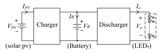
Figure 1.
Block diagram of solar power system for electronic signor street-lighting application.
Since the proposed power system adopts PV sources as its input source, the one needs the charger and discharger for electronic sign or streetlight application. The output voltage of solar power source is less than or greater than that of battery (8 V~12 V). Therefore, it simultaneously needs a step-up and step-down converter, such as buck-boost, ‘cuk, zeta and sepic converter [11,12,13]. As compared with ‘cuk, zeta and sepic converter, buck-boost converter possesses a simpler circuit topology. It is chosen as the charger for battery system, as shown in Figure 2. Since the flyback converter possesses many merits, which are a simpler circuit topology, wider ranges of voltage ratio between input voltage and output voltage and a lower cost, it can be applied to the solar power system or battery system. Therefore, the proposed power system can adopt buck-boost converter and flyback converter to implement battery charging and discharging functions, simultaneously, as shown in Figure 3.
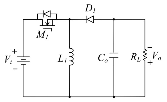
Figure 2.
Schematic diagram of buck-boost converter for battery charging applications.
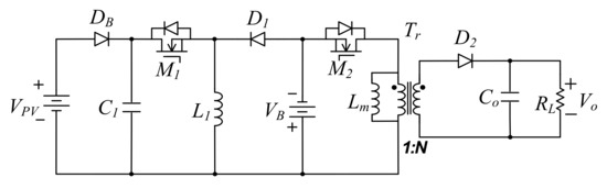
Figure 3.
Schematic diagram of buck-boost/flyback hybrid converter for battery charging and discharging applications.
When the proposed power system uses the flyback converter as the discharger, the leakage inductor of transformer will induce a spike voltage across switch. As a result, it will generate an extra switching loss. To avoid this problem, an active clamp circuit can be added into the flyback converter to recover leakage inductor energy [14,15,16,17], as shown in Figure 4. In order to simply circuit topology, switches of the charger and discharger can be respectively integrated, as shown in Figure 5. From Figure 5, the proposed hybrid converter can use a less component count to implement the battery charging and discharging functions, simultaneously. Therefore, the proposed power system can reduce cost, weight and size. Furthermore, the proposed one can be operated in ZVS at turn-on transition to increase conversion efficiency. It is suitable for a PV power system.
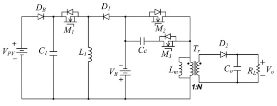
Figure 4.
Schematic diagram of buck-boost/flyback converter with active clamp circuit for solar power applications.
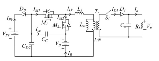
Figure 5.
Schematic diagram of the proposed hybrid converter for solar power applications.
2. Derivation of the Proposed Hybrid Converter
The proposed hybrid converter adopts a buck-boost converter as the battery charger and a flyback converter as the battery discharger, as shown in Figure 4. In order to simplify the proposed power system, a bidirectional buck-boost converter is used and an active clamp circuit is introduced into flyback converter to increase conversion efficiency, as shown in Figure 6. From Figure 6, since the battery charger and discharger in the proposed power system are operated in complementary, switch S1 is added into the proposed one to keep the battery charging and discharging functions. When switch S1 is regarded as the operational mode switch, switches M2 and M3 shown in Figure 6 can be merged as a switch M2 illustrated in Figure 5, while switches M1 and M4 can be merged as a switch M1. The inductor L1 can be also merged with the magnetizing inductor Lm of transformer. With this approach, the proposed power system can use a less component count to achieve the battery charging and discharging functions.
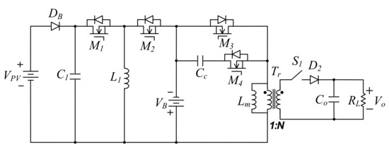
Figure 6.
Schematic diagram of the convention bidirectional buck-boost/flyback hybrid converter for solar power applications.
When the proposed power system is operated in the charging mode, switch S1 is turned off. The equivalent circuit of the proposed one is the same as a buck-boost converter, as shown in Figure 7a. In Figure 7a, the magnetizing inductor of transformer Tr is respected as the inductor of the buck-boost one, where topology of the proposed hybrid converter operated in the charging mode is highlighted with thick line. When the proposed one is operated in discharging mode, switch S1 is turned on, its equivalent circuit is the same as active clamp flyback converter, as shown in Figure 7b. In Figure 7b, the proposed hybrid one is highlighted with thick line. Therefore, the proposed power system can be respectively operated in different modes by the operational conditions of switch S1.
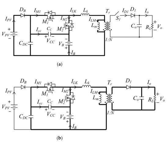
Figure 7.
Schematic diagram of the proposed hybrid converter operated in (a) the charging mode, and (b) the discharging mode.
3. Operational Principle of the Proposed Power System
The proposed hybrid converter can be divided into two operational modes: the charging mode and the discharging mode. Its equivalent circuit of the different operational modes is shown in Figure 7. Since the proposed hybrid converter can be operated in two different modes, its operational principle for each operational mode is also described in the following, respectively.
The charging mode
When the proposed hybrid converter is operated in the charging mode, its operational modes can be divided into 6 modes. The equivalent circuit of each operational mode and conceptual waveforms are plotted in Figure 8 and Figure 9, respectively. The power flow of each operational mode in the proposed hybrid converter is highlighted with thick line, as shown in Figure 9. In the following, each operational mode is briefly described.
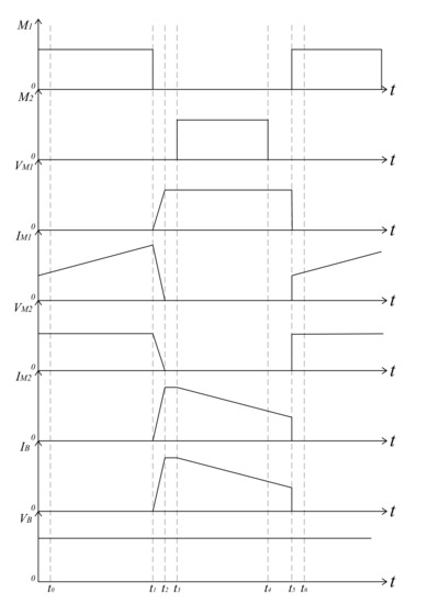
Figure 8.
Conceptual waveforms of the propose hybrid converter operated in the charging mode.
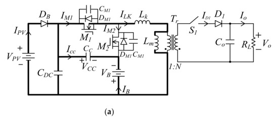
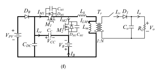
Figure 9.
Equivalent circuit of the proposed hybrid converter operated in the charging mode over one switching cycle; (a) Mode 1 (t0 ≤ t < t1); (b) Mode 2 (t1 ≤ t < t2); (c) Mode 3 (t2 ≤ t < t3); (d) Mode 4 (t3 ≤ t < t4); (e) Mode 5 (t4 ≤ t < t5); (f) Mode 6 (t5 ≤ t < t6).
Mode 1 [Figure 9a: t0 ≤ t < t1]: Before t0, switch M1 is in the turn-on state and switch M2 is in the turn-off state. During this time interval, switch current IM1 abruptly increases from 0A to the initial value of inductor Lm operated in continuous condition mode (CCM). When t = t0, switch M1 is still in the turn-on state, and M2 is kept in the turn-off state. Since inductance Lm is further greater than Lk, voltage VPV is approximately applied to inductance Lm. During this time interval, inductor Lm is in the stored energy state. Inductor current ILm linearly increases. The charging current IB equals 0A.
Mode 2 [Figure 9b: t1 ≤ t < t2]: At t = t1, switch M1 is turned off and switch M2 is still in the turn-off state. During this time interval, capacitor voltage VCM2 is discharging from (VPV + VB) to 0V, while VCM1 is charged from 0V to (VPV + VB). Within this mode, switch current IM1 abruptly decreases from the maximum value to 0A, and current IM2 quickly increases from 0V to the maximum value.
Mode 3 [Figure 9c: t2 ≤ t < t3]: At t = t2, body diode DM2 is in the forwardly bias state. Energy stored in magnetizing inductor Lm is released through battery and body diode DM2. Inductor current ILm linearly reduces. The battery is in the charging state.
Mode 4 [Figure 9d: t3 ≤ t < t4]: At t3, switch M2 is turned on and M1 is kept in the turn-off state. Since body diode DM2 is forwardly biased before t = t3, switch M2 is operated at ZVS at turn-on transition. Energy stored in magnetizing inductor Lm is still in the released energy state. Current ILm is equal to charging current IB, and its value linearly increases.
Mode 5 [Figure 9e: t4 ≤ t < t5]: At t = t4, switch M2 is turned off, and M1 is kept at the turn-off state. Since energy stored in inductor current ILm is released through battery and body diode DM2, switch voltage VM1 is kept at 0V. Capacitor voltage VCM1 is also kept at (VPV + VB). Inductor current ILm linearly reduces.
Mode 6 [Figure 9f: t5 ≤ t < t6]: At t = t5, switch M1 is turned on, and M2 is kept in the turn-off state. Due to body diode DM2 is in the forwardly bias state before t = t5, switch voltage VM1 abruptly varies from (VPV + VB) to 0V, switch voltage VM2 fast changes from 0V to (VPV + VB). Switch current IM1 suddenly increases to the initial value when the proposed converter is operated in CCM. Switch current IM2 and battery current IB simultaneously decreases to 0A. Since this time interval is very short, current IM1 is kept at the initial value and current IM2 and battery current IB are sustained at 0A. When t = t6, a new switching cycle will start.
The discharging mode
When the proposed hybrid converter is operated in the discharging mode during the night time, PV arrays does not generate power to supply battery. Furthermore, the proposed one with battery is required to supply energy to lighting system. According to the previously requirements, switch S1 is turned on and PV arrays are not to supply power to load by diode DB. Its equivalent circuit is implemented by flyback with active clamp circuit, as shown in Figure 7b. When the proposed hybrid converter is formed with the active clamp flyback converter, its operational mode is divided into eight modes. Its key component waveform is illustrated in Figure 10. In addition, equivalent circuit of each operational mode is depicted in Figure 11. In the following, each operational mode is described briefly.
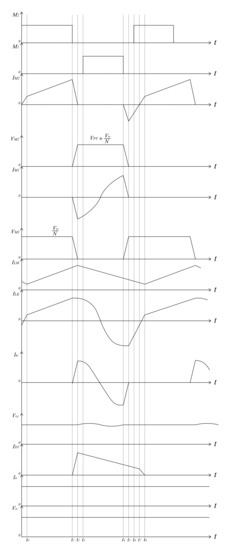
Figure 10.
Conceptual waveforms of the propose hybrid converter operated in the discharging mode.
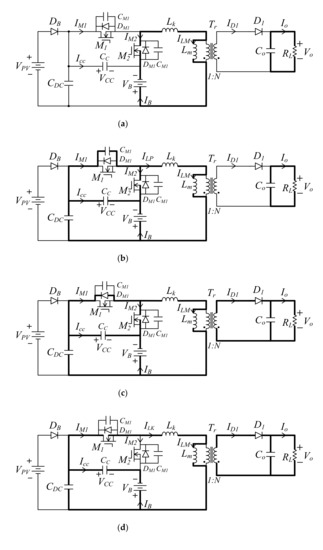
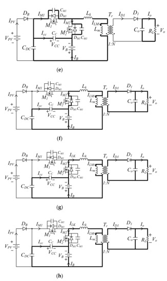
Figure 11.
Equivalent circuit of the proposed hybrid converter operated in the discharging mode over one switching cycle. (a) Mode 1 (t0 ≤ t < t1); (b) Mode 2 (t1 ≤ t < t2); (c) Mode 3 (t2 ≤ t < t3); (d) Mode 4 (t3 ≤ t < t4); (e) Mode 5 (t4 ≤ t < t5); (f) Mode 6 (t5 ≤ t < t6); (g) Mode 7 (t6 ≤ t < t7); (h) Mode 8 (t7 ≤ t < t8).
Mode 1 [Figure 11a: t0 ≤ t < t1]: Before t0, switch M2 is in the turn-on state and switch M1 is in the turn-off state. Switch current IM2 fast varies from 0A to the initial value of inductor Lm in the proposed converter operated in CCM. When t = t0, switch M2 is still in the turn-on state, and M1 is kept in the turn-off state. Switch current IM2 is equal to the initial value of inductor current ILm. During this time interval, magnetizing inductor Lm is in the stored energy state. Inductor current ILm linearly increases. Since diode D1 is reversely biased, load power is supplied by output capacitor Co.
Mode 2 [Figure 11b: t1 ≤ t < t2]: At t1, switch M2 is turned off and switch M1 is still in the turn-off state. Since inductor current ILK must be operated in the continuous condition through capacitor CM1 and CDC, Capacitor CM1 is discharged and its voltage VM1 varies from (Vo/N + VB) to 0V. Within this mode, capacitor Co supplies power to load. Switch current IM2 abruptly decreases to 0A, while current IM1 suddenly reduced to the negative maximum value. Capacitor current ICC also varies from 0V to its maximum value.
Mode 3 [Figure 11c: t2 ≤ t < t3]: When t = t2, body diode DM1 is forwardly biased and diode D1 is also in the forwardly bias. Inductor voltage VLm is clamped at (−Vo/N). During this time interval, leakage inductor Lk and capacitor CC form a resonant network. Inductor current ILk varies with the resonant form from the maximum value to the negative maximum value. Energy stored in the magnetizing inductor Lm is released through secondary winding of transformer Tr and diode D1 to load.
Mode 4 [Figure 11d: t3 ≤ t < t4]: At t = t3, switch M1 is turned on and M2 is kept in the turn-off state. Because body diode DM1 is in the forwardly bias state before t = t3, switch M1 is operated with ZVS at turn-on transition. Within this mode, inductor Lk and capacitor Cc connects in series to generate the resonance. Inductor current ILk is still in the resonant state, and current ILm linearly reduce to release the energy stored in the magnetizing inductor Lm.
Mode 5 [Figure 11e: t4 ≤ t < t5]: At t4, switch M1 is turned off, and M2 is kept at the turn-off state. Since capacitor CM1 enters the charging state, capacitor voltage VM1 varies from 0V to (Vo/N + VB). Moreover, capacitor voltage VM2 works in the discharging state, voltage VM2 change from (Vo/N + VB) to 0V. Within this mode, energy stored in the magnetizing inductor Lm releases through diode D1 to load. Inductor current ILm linearly reduces.
Mode 6 [Figure 11f: t5 ≤ t < t6]: When t = t5, capacitor voltage VM1 is clamped at (Vo/N + VB), while voltage VM2 is kept at 0V. At the moment, body diode DM2 is forwardly biased. During this time interval, inductor current ILk equals to current IM2. Their values abruptly varies from the negative maximum value to 0V. The magnetizing inductor Lm is still in the discharging energy state, and its current ILm linearly decreases.
Mode 7 [Figure 11g: t6 ≤ t < t7]: When t = t6, switch M2 is turned on, and switch M1 is still kept in the turn-off state. Since body diode DM2 is in the forwardly bias state before t6, switch M2 is operated with ZVS at turn-on transition. During this time interval, current ILK (=IM2) changes from a negative value to 0V. The magnetizing inductor Lm is still in the released energy state through diode D1 to load. Its current ILm linearly reduces.
Mode 8 [Figure 11h: t7 ≤ t < t8]: At t7, switch M2 is in the turn-on state and M1 is in the turn-off state. During this time interval, inductor current ILK varies from 0A to the initial value. The magnetizing inductor Lm is kept in the released energy state. Therefore, current ILm linearly decreases. When operational mode is at the end of mode 8, one new switching cycle will start.
4. Design of the Proposed Hybrid Converter
The proposed hybrid converter includes a charger and discharger. When the proposed one is operated as the charger, its equivalent circuit is the same as buck-boost converter. Moreover, its equivalent circuit is formed with an active clamp flyback converter for the discharger. Since the proposed one is composed with charger and discharger, its design must satisfy requirements of each converter. In the following, each converter is briefly analyzed.
A. Charger: Buck-boost converter
Since the battery charger is adopted with buck-boost converter, its key parameters include duty ratio D11 and inductor Lm. Therefore, duty ratio D11 and inductor Lm are derived in the following.
A.1 Duty ratio D11
In the light day, the proposed hybrid converter is regarded as the charger. The power flows from PV arrays to battery. During switching cycle, battery voltage VB is almost kept at a constant value. For maximum power point tracking (MPPT) of solar power, the proposed one can regulate the charging current IB to implement MPPT. The maximum duty ratio D11(max) can be determined under the minimum output voltage VPV(min) of solar power and maximum battery voltage VB(max). Its relationship is expressed as
where Ts represents the period of the proposed hybrid converter. From (1), D11(max) can be derived by
In addition, maximum transfer ratio M11(max) can be obtained as
According to the above equations, when type of battery is selected, the maximum charging current IB(max) can be denoted. Moreover, the charging current IB can changed from its maximum charging current IB(max) to 0A by regulating duty ratio D11 of switch M1. The charging current IB is determined by MPPT of solar power.
A.2 Inductor Lm
In order to obtain the inductance Lm, the boundary inductance LmB, which is the inductor value of the proposed converter operated in the boundary of CCM and discontinuous condition mode (DCM). Its conceptual waveforms are illustrated in Figure 12. The average charging current IB(av) can be determined as
where ΔILm(max) represents a maximum current variation of inductor Lm. In (4), ΔILm(max) can be expressed by
where VPV is the output voltage of solar power and VB represents the battery voltage. According to (4) and (5), the charging current IB(av) can be obtained as
Figure 12.
Conceptual waveforms of inductor current ILm and charging current IB in the charger.
Since the maximum charging current IB(av)max occurs at the maximum battery voltage VB(max) and the minimum PV voltage VPV(min), the maximum charging current IB(av)max can be rewritten with
where D11(min) represents duty ratio from VB(max) to VPV(max). Since the charger is always operated in CCM, IB(av)max can be expressed by K1IB(max), where K1 varies from 0 to 1 and IB(max) is the maximum charging current. In general, K1 is set at 0.1~0.3. From (7), it can be seen that inductor Lm1 can be expressed as
A.3. selection of switches
Figure 7a shows the schematic diagram of the proposed hybrid converter operated in the charging mode. In order to determine voltage and is at the maximum value and battery voltage is at maximum value, voltage ratings of components in the proposed one can be determined. Maximum voltage stresses of and can be determined by
In addition, voltage stress of switch obtained as
When input voltage is at minimum value and battery voltage is at maximum value, the maximum rms current of switch can be illustrated by
where r is defined by (). The maximum rms current of switch can be derived as
Moreover, the maximum rms current of inductor can be obtained as
Discharger: Active clamp flyback converter
When the proposed boost converter is operated in the discharging mode, its equivalent circuit is composed by flyback converter with the active clamp circuit. For design of active clamp flyback converter, the important parameters include duty ratio D12, transformer Tr, active clamp capacitor CC and output capacitor Co. In the following, their designs are analyzed briefly.
B.1. Duty ratio D12
When the proposed hybrid converter uses flyback converter with the active clamp circuit to achieve soft-switching features, the active clamp circuit does not affect transfer ratio M12 of the proposed flyback converter. That is, transfer ratio M12 is the same as the conventional one. According to volt-second balance of inductor Lm, the following equation can be obtained by
where N (=N2/N1) is the turns ratio of transformer Tr. From (9), it can be found that transfer ratio M12 can be represented as
When the output to input voltage transfer ratio M12 is determined, duty ratio D12 can obtained by
In the (11), when N, Vo and VB are specified, duty ratio D12 can be determined.
B.2. Transformer Tr
In order to Design transformer Tr, turns ratio N and the magnetizing inductor Lm are important parameters. Since output current Io can be determined by inductance Lm and turns ratio N, their conceptual waveforms is shown in Figure 13. From Figure 13, it can be found that the average diode current ID1(av) is represented by
where is the variation value of inductor current . According to operational principle of the proposed hybrid converter, inductor current ΔILm2(max) is obtained with
where LMB2 is the magnetizing inductance of transformer Tr where the proposed hybrid converter is operated in the boundary of DCM and CCM.
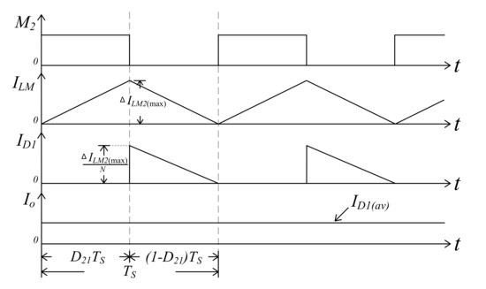
Figure 13.
Conceptual waveforms of inductor current ILm and output current Io in the discharger.
Since the proposed one adopts the active clamp circuit to achieve soft-switching features, its magnetizing inductor Lm2 is always operated in CCM. Therefore, the proposed one is designed in CCM under light load condition. The average current ID1(av) is equal to K2Io(max), where K2 range from 0 to 1 and Io(max) represents the maximum output current. According to (12) and (13), the magnetizing inductor Lm2 can be determined by
Since the magnetizing inductor Lm is separately operated in the charging and discharging modes, their inductances are derived with different values (Lm1 and Lm2), respectively. In order to design a proper inductance Lm, it is selected with the maximum value between Lm1 and Lm2.
In (10) and (11), when voltage VB and Vo are specified, turns ratio N is inversely proportional to duty ratio D12.Since a large duty ratio D12 corresponds to a smaller turns ratio N of transformer Tr. That is, lower current stresses are imposed on switches M1 and M2. However, in order to tolerate variations of load, battery voltage and component value, it is better to selected an operating ranges as D = 0.35~0.4. When duty ratio D12 is specified, turns ratio N can be determined.
B.3. Active clamp capacitor Cc
When the proposed hybrid converter adopts the active clamp to achieve soft-switching features, the active clamp capacitor CC can be used to recover energy trapped in leakage inductor Lk and help switch to achieve ZVS features. In order to obtain a wider range of soft-switching features, a half of resonant period is equal to or greater than turn-off time of switch M2 when capacitor Cc and leakage inductor Lk are formed as the resonant network. Therefore, capacitor Cc must satisfy the following inequality:
According to (15), capacitor CC can be expressed by
In (10), once leakage inductor Lk is specified, capacitor CC can be determined.
B.4. Output Capacitor Co
Since output capacitor Co is used to reduce ripple of output voltage Vo, its value must be large enough. The ripple voltage ΔVo across output capacitor Co is expressed as follows:
where Io(max) is the maximum output current. Therefore, output capacitor CO can be determined by
When the maximum output current Io(max), duty ratio D12, switching cycle TS and output ripple voltage ΔVo are specified, output capacitor Co can be determined by (18).
B.4. Selection of switches and diode
Figure 7a shows the schematic diagram of the proposed hybrid converter operated in the discharging mode. When battery voltage is under a maximum value situation, voltage rating of components can be determined. Maximum voltage stresses of switch and can be obtained as
Maximum voltage stress of diode can be expressed by
When the minimum battery voltage and output maximum current , the maximum rms current can be derived as
The maximum rms current is expressed by
Moreover, the maximum rms current is indicated by
Since switch is turned off, inductor and capacitor form a resonant network. A half resonant period of the resonant network is equal to (1) . The current waveform of switch varies with cosine wave manner. According to the rms calculation method for the cosine wave, the maximum rms current can be obtained by
where is cut the minimum battery voltage and expresses the maximum current of inductor . When the proposed hybrid converter is operated in the heavy load condition, current is approximately equal to [].
B.5. Power losses analysis
Since the proposed hybrid converter is operated in the charging mode, the proposed one is operated with hard-switching manner.Its power loss analysis is the same as the conventional buck converter.
The power loss analysis is neglected in this paper. When the proposed one is operated in the discharging mode, the active clamp capacitor can be used to recover the energy strapped in leakage inductor to increase conversion efficiency of the proposed one. Therefore, the power loss analysis is described for the proposed one operated in the discharging mode. When the proposed one is operated in the discharging mode, power loss includes losses of switches, diode and core. In the following, power loss analysis is derived.
(1). Losses of switches
The losses of switches include switching loss and conduction loss. Figure 14 shows the conceptual waveforms of switching losses for switches and . Since switches and is operated with ZVS at turn-on transition, their switching loss is only induced at turn-off transition of switches. Therefore, switching losses of switches and can be expressed by
where is equal to []. The conduction loss of switch or ) can be derived as
where is the rms current of each switch and represses a resistance of switch during turn-on state.
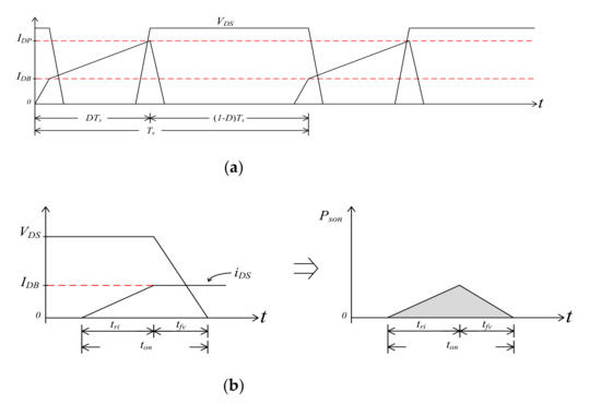
Figure 14.
Conceptual waveforms of switching loss during switch turn-on and turn-off transitions (a) during one switching cycle, (b) during turn-on transition (c) during turn-off transition.
(2). Loss of diode
The loss of diode is generated by the forward voltage when diode is in the forward biased state. The loss can be derived by
(3). Loss of core
The loss of core includes core loss and copper loss.The core loss of transformer is determined by the maximum flux density and core loss curve of core. The maximum flux density can be determined by
where N is the turns of primary winding and expresses the effective magnetic path length, indicates air gap length and permeability. When is determined, the core loss coefficient can be obtained through core loss curve of core. The core loss is determined as
where is the effective core volume of core. Moreover, copper loss can be derived by
where is the resistance coefficient of wire gauge of primary winding, represses the total length of turns of primary winding, is the resistance coefficient of wire gauge of secondary winding and indicates the total length of turns of secondary winding.
A. Block diagram of control method of the proposed hybrid converter
In order to control the proposed hybrid converter, a microcontroller and pulse-width modulation integrated circuit (PWM IC) are adopted in the proposed systems, as shown in Figure 15. In Figure 15, the microcontroller is used to implement maximum power point tracking (MPPT) of solar power, manages battery charging, controls battery charging current and perform battery protection. Moreover, the PWM IC is adopted to regulate output voltage Vo. For MPPT, this paper uses the perturb-and-observe method to execute the MPPT of solar power. In order to match the MPPT of solar power, charger adopts constant current (CC) method to implement battery charging.
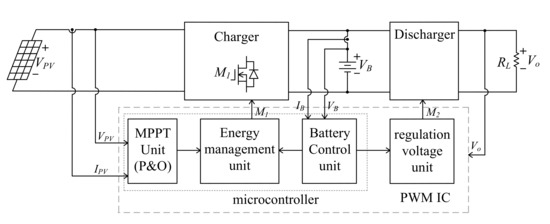
Figure 15.
Block diagram of the proposed hybrid converter for solar power system applications.
B. Performances comparison between the proposed hybrid converter and the conventional counterpart converter
In general, key components of switching power supply include the switch, diode, magnetic device, capacitor, printed circuit board (PCB), control IC, driving circuit, filter and resistor, and so on. According to the technical report of the Industrial Economics and Knowledge Center (IEK) in Taiwan, cost of each component in switching power supply is illustrated in Table 1. From Table 1, it can be found that switch, capacitor, magnetic device, diode and driving circuit possess higher cost ratio in the switching power supply. Table 2 lists the component counts comparison between the proposed hybrid converter and the conventional counterpart converter. Since the conventional counterpart converter shown in Figure 4 includes three switches, two magnetic devices, two diodes and two sets of driving circuits, the proposed hybrid converter can reduce component usage and increase an extra switch S1 usage. When the proposed one reduces one switch usage, it can obtain a cost reduction of 6.7%. In addition, the reduction magnetic device, diode and driving circuit usage of the proposed one can acquire a cost reduction of 8%, 5% and 6%, respectively. In order to reduce component counts, the proposed one increases a cost of 3~6.7%. From Table 2, it can be found that the proposed one can reduce cost of 19–22.7%.

Table 1.
Total cost analysis of switching power supply (data from Industrial Economics and Knowledge Center (IEK) in Taiwan).
Table 2.
Component count comparison between the proposed hybrid converter and the conventional counterpart converter.
5. Experimental Results
The proposed hybrid converter used solar power as its input source. Specifications of solar power are listed in Table 3. The following specifications were implemented.
Table 3.
Specification of the solar power supplied by solar power manufacturer.
A. Charger: Buck-boost converter
- Input voltage VPV: DC 17.5 V~20.6 V (solar power),
- Switching frequency fs1: 50 kHz,
- Output voltage VB: DC 8 V~12 V (lithium battery:3.2 Ah), and
- Maximum charging current IB(max): 3.2 Ah
B. Discharger: flyback converter
- Input voltage VB: DC 8 V~12 V (lithium battery:3.2 Ah),
- Switching frequency fs2: 50 kHz,
- Output voltage Vo: DC 10 V, and
- Maximum output current Io(max): 2 A.
According to the previously specifications and design of the proposed hybrid converter, inductor Lm, turns ratio N and active clamp capacitor CC could be determined. Table 4 illustrates parameters of components of the proposed hybrid converter. According to operational conditions of the proposed one, current and voltage stresses could be determined. From Table 4, it can be obtained that the magnetizing inductor Lm equaled 660 μH and turns ratio N was equal to 2. When transformer Tr was wound with the magnetizing inductor Lm of 660 μH, leakage inductor Lk was measured and its value was 12.5 μH. Therefore, the active capacitor CC was calculated and its value was 1.62 μF. Capacitor CC is adopted with 1.5 μF. In addition, current and voltage stresses of the proposed hybrid converter and the conventional counterpart converter are listed in Table 5. From Table 5, it can be found that although component stress of the proposed hybrid converter was higher than that of the conventional counterpart converter, it could use fewer component counters to achieve the charging and discharging functions. The switch S1 could adopt lower current and voltage stresses to change the charging mode or discharging mode of the proposed one. Furthermore, the components of power stage in the proposed hybrid converter were determined as follows:
Table 4.
Parameters of components in the proposed hybrid converter.
Table 5.
Current and voltage stresses of components between the proposed hybrid converter and the counterpart converter.
- Switches M1, M2: AoW2918,
- Diode D1: STPS10L60D,
- Switches S1: AoW2918,
- Transformer Tr: EE-33 core, and
- Output capacitor Co: 47 μF/25 V.
Figure 16 shows the photo of the proposed hybrid prototype converter. The hardware dimension of the proposed hybrid converter was about 100 × 60 mm2. The circuit layout safety distance was set at 5 mm around outside of each component. According to the requirement of safety distance of each component, circuit layout area comparison between the proposed hybrid converter and the conventional counterpart converter is listed in Table 6. When switch M1 was adopted with AoW2918, its package wasTO220. According to dimension of TO220 package, component dimension was 10 × 5 mm2. In order to consider safety distance between two components, circuit layout dimension was considered with 20 × 15 mm2. Although a component with a heat sink could increase its power processing capacity, its circuit layout dimension was increased. The heat sink dimension for TO220 package was 15 × 10 mm2. Therefore, switch with heat sink needed 25 × 20 mm2 for switch layout dimension. According to the above requirement to layout the proposed hybrid converter and the conventional counterpart converter, their circuit layout area is respectively calculated in the Table 6. From Table 6, it can be found that the proposed hybrid converter needed a circuit layout area of 6000 mm2, while the conventional counterpart converter needed that of 9000 mm2. Therefore, the proposed one could reduce circuit layout area by 3000 mm2. The power density of the proposed one could increase about 1.5 times.
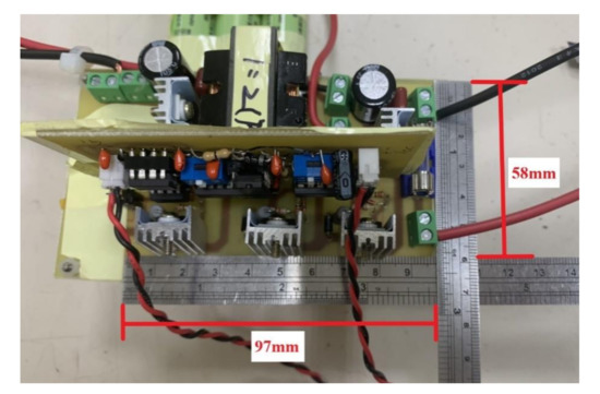
Figure 16.
Photo of the proposed hybrid converter prototype.
Table 6.
Layout area comparison between the propose hybrid converter and the conventional counterpart converter.
The proposed hybrid converter used solar power to charge the battery with CC. The MPPT and battery charging with CC must be implemented. When solar power was used as input voltage source, the proposed hybrid converter adopted the perturb-and-observe method to implement MPPT. Measured voltage VPV, current IPV, and power PPV waveforms of solar power is shown in Figure 17. Figure 17a illustrates those waveforms under PPV(max) = 15 W, while Figure 17b plots those waveforms under PPV(max) = 30 W. From Figure 17, it can be obtained that tracking time T of solar power was about 200 ms. Figure 18 shows measured gate voltage M1 of switch M1 and charging current IB. Since capacitor CC connected with inductor Lm in series, they formed a resonant network through battery or capacitor CDC during switch M1 turn-on or turn-off interval, respectively. The measured charging current IB varied with a resonant waveform. Figure 18a shows those waveforms under the average charging current IB(av) = 0.7 A. Moreover, Figure 18b illustrates those waveforms under IB(av) = 3 A.
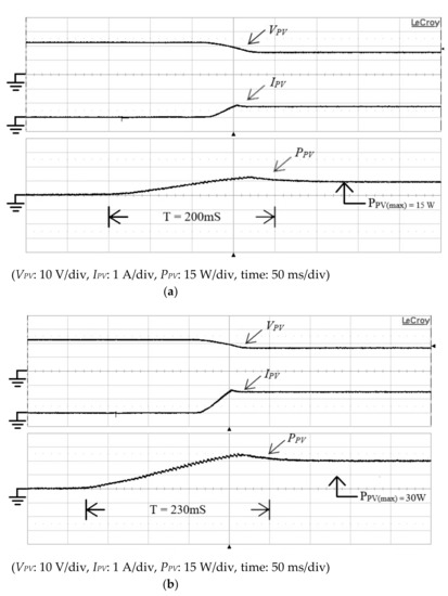
Figure 17.
Measured voltage VPV, current IPV and power PPV of solar power under maximum power point tracking (MPPT): (a) PPV(max) = 15 W, and (b) PPV(max) = 30 W.
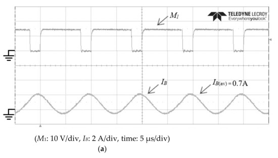
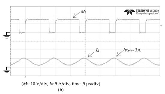
Figure 18.
Measured gate voltage M1 and charging current IB of the proposed hybrid converter operated in the charging mode: (a) under the average charging current IB(av) = 0.7 A, and (b) under IB(av) = 3 A.
Since the proposed hybrid converter was operated in the discharging mode, switches M1 and M2 were operated with ZVS at turn-on transition. When the proposed hybrid converter was operated in the discharging mode, measured switch voltages VM1, VM2 and currents IM1, IM2 waveforms of the proposed hybrid converter are shown in Figure 19. Figure 19a,b show those waveforms under 10% of full-load condition, while Figure 20a,b illustrate those waveforms under 15% of full-load condition. From Figure 19 and Figure 20, it can be found that switch M1 and M2 were operated with ZVS at turn-on transition under 10–15% of full-load condition, simultaneously. Figure 21 illustrates measured output voltage Vo and output current Io under step-load change between 0% of full-load and 100% of full-load conditions, from which it can be obtained that the voltage regulation of output voltage Vo was limited within ±1%.
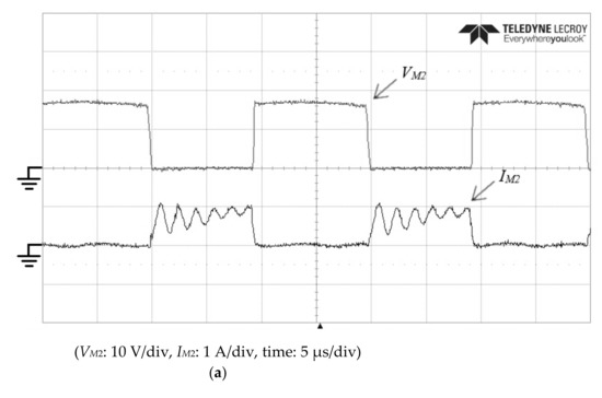
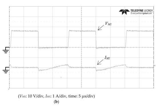
Figure 19.
Measured voltage VM1, VM2 and currents IM1, IM2 waveforms of the proposed hybrid converter operated in the discharging mode: (a) voltage VM2 and current IM2, and (b) voltage VM1 and current IM1 under 10% of full-load condition.
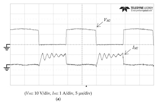
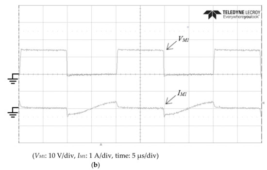
Figure 20.
Measured voltage VM1, VM2 and currents IM1, IM2 of the proposed hybrid converter operated in the discharging mode: (a) voltage VM2 and current IM2, and (b) voltage VM1 and current IM1 under 15% of full-load condition.
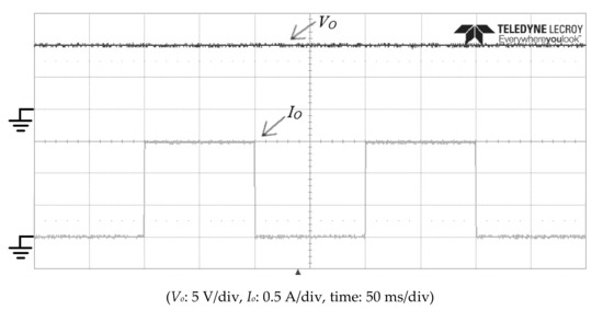
Figure 21.
Measured output voltage Vo and output currents Io waveforms of the proposed hybrid converter operated in the discharging mode under step-load changes between 0% and 100% of full-load condition.
Comparison of conversion efficiency between flyback converter with hard-switching circuit and with the proposed active clamp circuit from light load to heavy load is shown in Figure 22, illustrating that the efficiency of the proposed converter is higher than that of hard-switching one. Its efficiency was 85% under full-load condition. According to component selection of the proposed hybrid converter, key component parameters are listed in Table 7. Power loss analysis of the proposed hybrid converter under full-load condition is illustrated in Table 8. Total power losses included switch, diode, transformer and driving circuit in the proposed hybrid one. The driving circuit loss was measured by oscillator and voltage Vcc is 12 V and current Icc was17.7 mA. The driving circuit loss PDC was 0.21 W. Since switches M1 and M2 were operated with ZVS at turn-on transition, their switching loss only considered switching loss at turn-off transition. According to the maximum operational current and voltage of switch, diode and transformer in the proposed hybrid converter, losses of each component are listed in Table 8. Switch S1 was one time in the turn-on or turn-off state during a day. Its loss was only conduction loss. According to (33) and Table 4, maximum flux density Bm can be determined and its value was 200 mT. Figure 23 shows the core loss curves of transformer Tr manufactured by PC95 material of TDK. When Bm = 200 mT, core coefficient Cp is equal to 110 mW/cm3. Effective core volume Ve of transformer Tr was equal to 8.03 cm3. The core loss could be determined and its value PcTr = 0.88 W. In addition, copper loss PcpTr could be obtained by (35). Since ID1(rms) = IS1(rms) = 2.55 A, ILm2(rms) = 6.5 A, Rdc1lm1 = 0.027 Ω and Rdc2lm2 = 0.062 Ω, copper loss PcpTr equaled 1.54 W. The conversion efficiency of the proposed hybrid converter operated in the discharging mode was 86.6% under full-load condition. The practical conversion was 85%. The stray loss of the proposed hybrid converter was 1.6%.
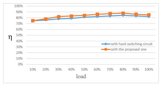
Figure 22.
Comparison conversion efficiency between the conventional hard-switching flyback converter and the proposed one from light load to heavy load for operating in the discharging mode.
Table 7.
Key component parameters of the proposed hybrid converter.
Table 8.
Power loss analysis of the proposed hybrid converter under = 12 V and output maximum current .
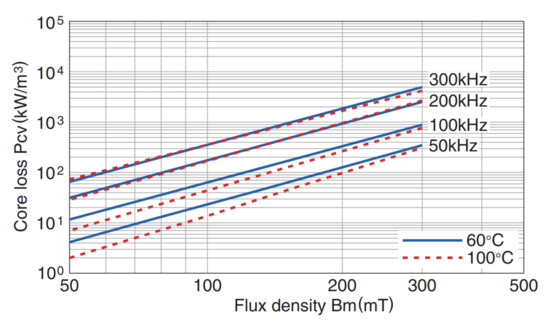
Figure 23.
Core loss (mW/cm3) curves of transformer Tr manufactured by PC95 material of TDK.
6. Conclusions
The proposed hybrid converter is consisted of buck-boost converter and active flyback converter to implement battery charger and discharger. Circuit derivation of the proposed hybrid converter is presented in this paper for decreasing component count. Moreover, operational principle, steady-state analysis, design and power loss analysis of the proposed hybrid converter have been described in detail. As compared with the conventional counterparts with hard-switching circuit, the proposed one can increase conversion efficiency of 4% and achieve efficiency of 85% under full load condition when the proposed one is operated in the discharging mode. In addition, cost and power density comparison between the proposed hybrid converter and the conventional counterpart converter, the proposed hybrid one can reduce cost of 19–22.7% and power density of the proposed one can increase about 1.5 times. An experimental prototype has been implemented for lithium battery of 12 V/3.2 Ah and for LED lighting of 10 V/2 A. It can verify the feasibility of the proposed hybrid converter. It is suitable for solar power applications.
Author Contributions
Conceptualization, methodology, and writing—original draft preparation, S.-Y.T.; writing—review and editing, J.-H.F. All authors have read and agreed to the published version of the manuscript.
Funding
This research was funded by Ministry of Science and Technology (MOST) in Taiwan grant number MOST 109-2622-E-182-003-cc3.
Conflicts of Interest
The authors declare no conflict of interest.
References
- Alghaythi, M.L.; O’Connell, R.M.; Islam, N.E.; Khan, M.M.S.; Guerrero, J.M. A High Step-Up Interleaved DC-DC Converter with Voltage Multiplier and Coupled Inductors for Renewable Energy Systems. IEEE Trans. Ind. Electron. 2020, 8, 123165–123174. [Google Scholar]
- Sahli, A.; Krim, F.; Laiband, A.; Alam, M.S.; Talbi, B. Energy management and power quality enhancement in grid-tied single-phase PV system using modified PUC converter. IET Renew. Power Gener. 2019, 13, 2512–2521. [Google Scholar] [CrossRef]
- Castro, I.; Vazquez, A.; Aller, D.G.; Arias, M.; Lamar, D.G.; Sebastian, J. On Supplying LEDs from Very Low DC Voltages with High-Frequency AC-LED Drivers. IEEE Trans. Power Electron. 2018, 34, 5711–5719. [Google Scholar] [CrossRef]
- Wang, Y.; Hu, X.; Guan, Y.; Xu, D. A Single-Stage LED Driver Based on Half-Bridge CLCL Resonant Converter and Buck–Boost Circuit. IEEE Trans. Ind. Appl. 2019, 7, 196–208. [Google Scholar] [CrossRef]
- Tsou, M.C.; Kuo, M.T. Optimal Combination Design of a Light Emitting Diode Matrix Applicable to a Single-Stage Flyback Driver. Energies 2020, 13, 5209. [Google Scholar] [CrossRef]
- Alonso, J.M.; Vina, J.; Vaquero, D.G.; Martinez, G.; Osorio, R. Analysis and design of the integrated double buck-boost converter as a highpower-factor driver for power-LED lamps. IEEE Trans. Ind. Electron. 2012, 59, 1689–1697. [Google Scholar] [CrossRef]
- Chen, Y.S.; Liang, T.J.; Chen, K.H.; Juang, J.N. Study and implementation of high frequency pulse LED driver with self-oscillating circuit. In Proceedings of the 2011 IEEE International Symposium of Circuits and Systems (ISCAS), Rio de Janeiro, Brazil, 15–18 May 2011; pp. 498–501. [Google Scholar]
- Wang, Y.; Zhang, S.; Alonso, J.M.; Liu, X.; Xu, D. A high efficiency driver for high-brightness white LED lamp. In Proceedings of the IEEE TENCON Conference, Jeju Island, Korea, 28–31 October 2018. [Google Scholar]
- Lee, S.W.; Do, H.L. A Single-Switch AC–DC LED Driver Based on a Boost-Flyback PFC Converter with Lossless Snubber. IEEE Trans.Power Electron. 2016, 32, 1375–1384. [Google Scholar] [CrossRef]
- Cheng, C.A.; Chang, C.H.; Chung, T.Y.; Yang, L. Design and Implementation of a Single-Stage Driver for Supplying an LED Street-Lighting Module With Power Factor Corrections. IEEE Trans. Power Electron. 2015, 30, 956–966. [Google Scholar] [CrossRef]
- Chen, X.; Pise, A.A.; Elmes, J.; Bataresh, I. Ultra-Highly Efficient Low-Power Bidirectional Cascaded Buck-Boost Converter for Portable PV-Battery-Devices Applications. IEEE Trans. Ind. Appl. 2019, 55, 3989–4000. [Google Scholar] [CrossRef]
- Kim, K.D.; Lee, H.M.; Hong, S.W.; Cho, G.H. A Non-inverting Buck-Boost Converter with State-Based Current Control for Li-ion Battery Management in Mobile Applications. IEEE Trans Ind. Electron. 2019, 66, 9623–9627. [Google Scholar] [CrossRef]
- Pouladi, F.; Farzanehfard, H.; Adib, E. Battery Operated Soft Switching Resonant Buck–Boost LED Driver with Single Magnetic Element. IEEE Trans Power Electron. 2019, 34, 2704–2711. [Google Scholar] [CrossRef]
- Rezaei, M.A.; Lee, K.J.; Huang, A.Q. A High-Efficiency Flyback Micro-inverter with a New Adaptive Snubber for Photovoltaic Applications. IEEE Int. Power Electron. 2016, 31, 318–327. [Google Scholar] [CrossRef]
- Kwon, M.; Kwon, B.H. High step-up active-clamp converter with input-current doubler and output-voltage doubler for fuel cell power systems. IEEE Trans. Power Electron. 2009, 24, 108–115. [Google Scholar] [CrossRef]
- Silva, M.P.; Perez, D.S.; Benitez, O.M.R.; Valdes, L.G.V.; Sanchez, A.C.; Aldaco, S.E.D.L.; Garcia, C.C.; Benitez, Y.I.S.; Ponce, R.E.L.; Tapia, J.A.A. Flyback Converter for Solid-State Lighting Applications with Partial Energy Processing. Energies 2021, 10, 60. [Google Scholar]
- Tseng, S.Y.; Hauang, P.J.; Wu, D.H. Power Factor Corrector with Bridgeless Flyback Converter for DC Loads Applications. Energies 2018, 11, 3096. [Google Scholar] [CrossRef]
Publisher’s Note: MDPI stays neutral with regard to jurisdictional claims in published maps and institutional affiliations. |
© 2021 by the authors. Licensee MDPI, Basel, Switzerland. This article is an open access article distributed under the terms and conditions of the Creative Commons Attribution (CC BY) license (http://creativecommons.org/licenses/by/4.0/).