Article

Hole Injection Role of p-Type Conjugated Polymer Nanolayers in Phosphorescent Organic Light-Emitting Devices

1
Organic Nanoelectronics Laboratory, KNU Institute for Nanophotonics Applications (KINPA), Department of Chemical Engineering, School of Applied Chemical Engineering, Kyungpook National University, Daegu 41566, Korea
2
Research Institute of Environmental Science & Technology, Kyungpook National University, Daegu 41566, Korea
*
Author to whom correspondence should be addressed.
Electronics 2021, 10(18), 2283; https://doi.org/10.3390/electronics10182283
Submission received: 26 August 2021 / Revised: 8 September 2021 / Accepted: 12 September 2021 / Published: 17 September 2021
(This article belongs to the Special Issue Advanced Displays: OLED, QLED, and Beyond)

Abstract

:
Here, we report the hole injection role of p-type conjugated polymer layer in phosphorescent organic light-emitting devices (OLEDs). Poly(3-hexylthiophene) (P3HT) nanolayers (thickness = ~1 nm thick), which were subjected to thermal annealing at 140 °C by varying annealing time, were inserted between indium tin oxide (ITO) anodes and hole transport layers (N,N′-bis(naphthalen-1-yl)-N,N′-bis(phenyl)-benzidine, NPB). The 1 nm-thick P3HT layers showed very weak absorption in the visible light range of 500~650 nm. The device results disclosed that the presence of P3HT layers were just able to improve the charge injection of OLEDs leading to an enhanced luminance irrespective of thermal annealing condition. The highest luminance and efficiency were achieved for the OLEDs with the P3HT layers annealed at 140 °C for 10 min. Further annealing for 30 min resulted in turn-down of device performances. The emission color was almost unchanged by the presence of P3HT layers even though the color coordinates were marginally fluctuated according to the annealing time. The present result delivers the possibility to use p-type conjugated polymers (i.e., P3HT) as a hole injection layer in OLEDs.

1. Introduction

Since the first report on organic multilayer structures, organic light-emitting devices (OLEDs) have been extensively studied and now successfully commercialized for various applications such as smart phones, smart watches, television sets, etc. [1,2,3,4,5,6,7,8,9,10]. The successful commercialization of OLEDs can be ascribed to advances in organic semiconducting materials for both emission and charge transport layers [11,12,13,14,15,16,17,18]. In particular, optimization of device structures including the thickness of organic multilayers have greatly improved the performance of OLEDs [19,20,21,22]. In terms of efficiency, phosphorescent emitters such as iridium-based small molecules, for example, tris(2-phenylpyridine)iridium(III) (Ir(ppy)3), contributed to effectively harnessing triplet excitons for visible light emission [23,24,25]. In addition, the approach of delayed fluorescence opened new gate toward high efficiency using fluorescent organic materials only [26,27,28,29,30].
However, the recently commercialized OLED displays consist of organic small molecules and are fabricated using thermal evaporation processes in a vacuum [31,32,33]. Therefore, the manufacturing cost of conventional OLEDs is high because of the expensive vacuum systems [34,35,36]. In addition, practical roll-to-roll processes, which are considered one of the most effective and competitive processes for organic devices compared to inorganic devices, cannot be utilized owing to such vacuum systems [37,38,39,40]. Accordingly, extensive studies have been carried out for solution-processed OLEDs by employing ink-jet printing processes [41,42,43].
For solution processes of OLEDs, all organic layers should be coated by wet-coating methods using soluble organic materials [44,45,46]. As the first hole injection layer that is typically coated on transparent indium tin oxide (ITO) electrodes, poly(3,4-ethylenedioxythiophene):poly(styrene sulfonate) (PEDOT:PSS) has been widely used for the last three decades [47,48,49]. However, it has been reported that the strong acidity of PEDOT:PSS can reduce the operation stability of OLEDs [50,51]. This consideration motivates development of various materials including copper thiocyanate (CuSCN) with good organic solvent resistance and high hole conductivity [52]. In particular, conjugated polymer-based electrolytes have been also studied as a hole injection layer [53,54,55]. However, less attention has been relatively paid to neutral conjugated polymers, which possess p-type semiconductor characteristics, as a hole injection layer in OLEDs.
In this work, we have attempted to use p-type conjugated polymer, well-known poly(3-hexylthiophene) (P3HT), as a hole injection layer for phosphorescent OLEDs. The major benefit of P3HT as a hole injection layer can be attributed to its highest occupied molecular orbital (HOMO) energy level (ca. −5.1 eV) that can effectively reduce the energy barrier of hole injection from indium tin oxide (ITO) anode (work function: ca. −4.8 eV) to hole transport layers (HOMO energy: ca. −5.4 eV typically), whereas the demerit of P3HT can be assigned to a possible absorption of visible light from OLEDs [56]. To minimize the adverse effect of absorbing electroluminescence from emission layers by the P3HT layers, the thickness of P3HT layers was controlled as low as possible (ca. 1 nm). The annealing temperature for the P3HT layers was set to 140 °C, which is slightly higher than the glass transition temperature (Tg) of P3HT (ca. 110 °C) [57]. To briefly investigate the thermal annealing effect, the P3HT layers were annealed at 140 °C by varying the annealing time. Results showed that the performance of OLEDs was certainly improved by introducing the P3HT layers between anodes and hole transport layers. In particular, the luminance and efficiency of devices were significantly enhanced by thermal annealing at 140 °C for 10 min.

2. Materials and Methods

2.1. Materials and Solutions

The P3HT polymer (weight-average molecular weight = 30 kDa, polydispersity index = 1.7, regioregularity > 96%) was used as received from Rieke Metals (Lincoln, Dearborn, MI, USA). N,N′-bis(naphthalen-1-yl)-N,N′-bis(phenyl)-benzidine (NPB), 4,4′-bis(carbazol-9-yl)biphenyl (CBP), tris(2-phenylpyridine)iridium(III) (Ir(ppy)3), and 2,2′,2″-(1,3,5-benzinetriyl)-tris(1-phenyl-1-H-benzimidazole) (TPBi) were purchased from Luminescence Technology Corp.(New Taipei city, Taiwan) and used without further purification. The P3HT solutions were prepared using chlorobenzene (CB) as a solvent at a solid concentration of ca. 1 mg/mL.

2.2. Device and Film Fabrication

To fabricate OLEDs, indium-tin oxide (ITO)-coated glass substrates were subjected to photolithography processes for patterning the ITO electrode (size = 8 × 12 mm). The patterned ITO-coated glasses were cleaned with acetone and isopropyl alcohol by utilizing an ultrasonic bath, followed by treating under UV-ozone (UVO) for 20 min (AH1700, 23 mW/cm2). On top of the UVO-treated ITO-glass substrates, the P3HT solutions were spun for 30 s at 1500 rpm and thermally annealed at 140 °C for 10 min and 30 min individually in an argon-filled glove box. The thermally treated P3HT-coated ITO-glass samples were mounted on a metal shadow mask and moved into a vacuum chamber system inside the argon-filled glove box. Note that the UVO-cleaned ITO-glasses without the P3HT layers were also mounted on the same metal shadow mask. When the base pressure of chamber reached ~1.0 × 10⁻⁶ torr, the NPB layer (thickness = 20 nm) was first deposited on the P3HT-coated ITO-glass substrates by thermal evaporation process. Next, NPB, CBP, Ir(ppy)3, and TPBi were sequentially evaporated to make multilayers. Finally, lithium fluoride (LiF) and aluminum (Al) were thermally evaporated to form electron injection layers and electrodes. The layer thickness of NPB, CBP, Ir(ppy)3, TPBi, LiF, and Al was 20, 37.6, 2.4, 40, 1, and 95 nm, respectively. All devices were stored inside the same glove box and loaded into a sample holder that is charged with argon for measurements.

2.3. Measurements

The optical absorption spectra of film samples were measured using a UV-visible spectrometer (Lambda 750, PerkinElmer). A surface profiler (DektakXT-E, Bruker) was used to measure the thickness of organic films and Al electrodes. The performances of OLEDs were measured using an OLED measurement system equipped with an electrometer (Keithley 2400) and spectroradiometers (PR650, PhotoResearch). The International Commission on Illumination (CIE) coordinates of emission color were automatically obtained from the PR650 system.

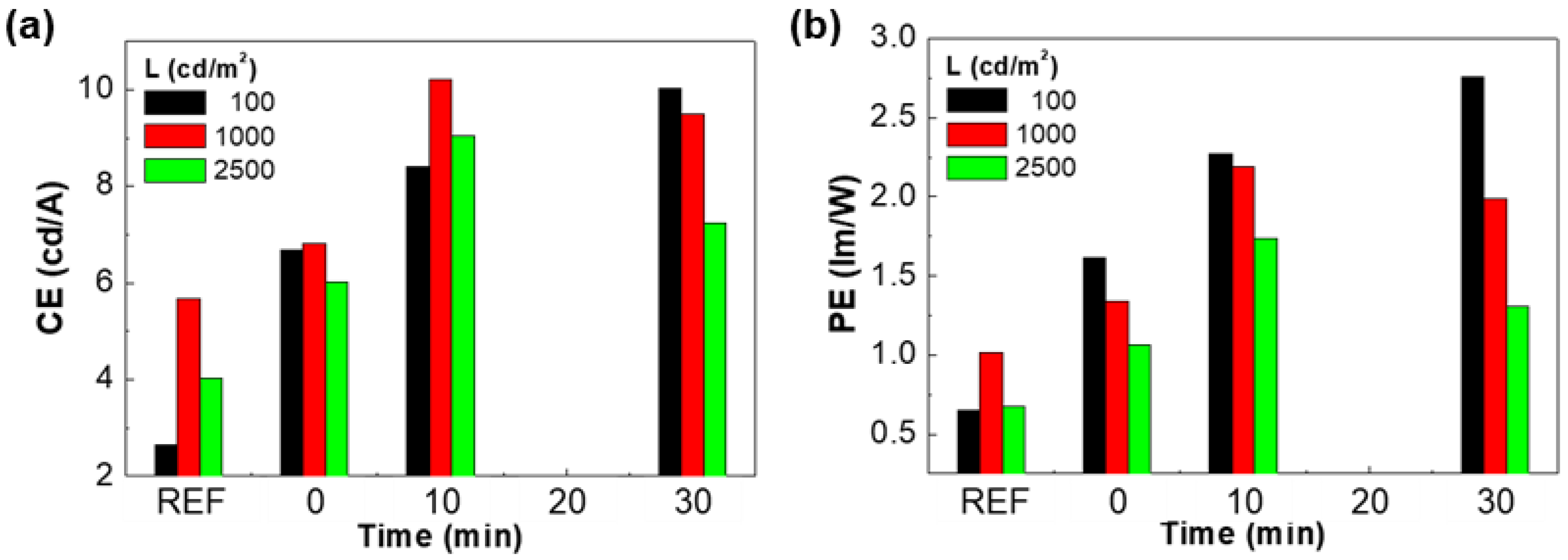
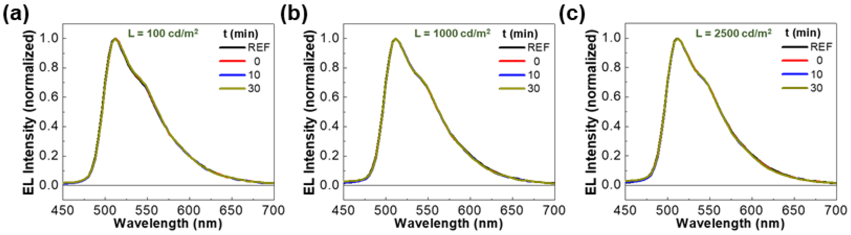
3. Results and Discussion

As shown in Figure 1a, the present OLEDs were fabricated with organic multilayers between the ITO and LiF/Al electrodes. Here, the P3HT layers are designed to play a hole injection role at the interfaces between the NPB layers and the ITO anodes. As illustrated in Figure 1b, the HOMO energy level of P3HT (5.1 eV) is expected to act as a bridge for mild hole injection from the ITO electrode to the NPB layer. The injected holes can transport through the NPB layer and reach the emission layer (CBP:Ir(ppy)3), while the injected electrons from the Al electrode via the LiF layer transport through the TPBi layer to the emission layer. It is noted that the TPBi layer does a hole blocking role in addition to the electron transport. The recombination of these holes and electrons results in the emission of green light. As observed from Figure 1c, the P3HT layer absorbs photons in the wavelength range of ca. 450~650 nm which corresponds to the electroluminescence (EL) range of emission layer in the present devices. However, it is regarded that the P3HT layer may very slightly absorb the green light emitted from the emission layer because the thickness (t) of P3HT layers is only ca. 1 nm (see the absorbance value in Figure 1c). Here it is worthy to note that the 1 nm-thick P3HT layers were well coated and covered all the area of the ITO-glass surfaces (see the inset photographs in Figure 1c).
The electrical and light emission characteristics of OLEDs were measured as shown in Figure 2. The current density-voltage (J–V) curves disclose that the insertion of P3HT layers could increase the current density of devices irrespective of annealing time. A close look into the J–V curves finds that the highest current density at 20 V was measured in the case of thermal annealing at 140 °C for 10 min. However, further annealing for 30 min resulted in the turn-down of current density despite still higher than the current density of reference device (without any P3HT layer). The luminance–voltage (L–V) curves in Figure 2b show that the highest luminance (7850 cd/m2 at 20 V) could be achieved in the case of thermal annealing (P3HT) for 10 min. However, the luminance (5900 cd/m2 at 20 V) was slightly lowered by further annealing (for 30 min). It is noted that the luminance was obviously higher for the OLED with the unannealed P3HT layer (0 min-OLED) than the reference device (REF-OLED), which is clearly observed from the luminance–current density (L–V) curves in Figure 2c. This result indicates that the performance of OLEDs could be improved by the presence of the 1 nm-thick P3HT layers.
To understand the effect of thermal annealing on the P3HT layers, the efficiency of OLEDs was plotted as shown in Figure 3. As observed from Figure 3a, over the entire luminance range, the current efficiency (CE) was higher for the OLEDs with the P3HT layers annealed at 140 °C than REF-OLED. Although the P3HT layer was unannealed, the current efficiency was noticeably improved from REF-OLED. Here, it is worthy to note that the highest current efficiency was measured for the OLED with the P3HT layer annealed at 140 °C for 30 min (30 min-OLED) at a low luminance range below ca. 680 cd/m2. However, as the luminance increased, the current efficiency of 30 min-OLED was quickly decreased and lower than that of the OLED with the P3HT layer annealed at 140 °C for 10 min (10 min-OLED), even though its level is still higher than REF-OLED and 0 min-OLED. The similar trend was observed for the luminous efficiency (LE) in Figure 3b. Here it is noted that the highest current efficiency and luminous efficiency at a high luminance range (>1000 cd/m2) were achieved by thermal annealing at 140 °C for 30 min. The present efficiency trend supports that the P3HT layers actually act as a hole injection layer and improve the performance of OLEDs.
For the detailed investigation, the efficiency of OLEDs at three different luminance levels was compared according to the annealing time. As shown in Figure 4a, the current efficiency of REF-OLED was 2.63 cd/A at 100 cd/m2 but it was noticeably increased to 6.66 cd/A at 100 cd/m2 for 0 min-OLED. The thermal annealing process at 140 °C for 10 min and 30 min further increased the current efficiency (at 100 cd/m2) up to 8.39 cd/A and to 10.01 cd/A, respectively. The similar increase in current efficiency at 1000 cd/m2 was obtained for both 0 min-OLED and 10 min-OLED, but the current efficiency of 30 min-OLED was slightly lowered from that of 10 min-OLED. The current efficiency gap between 10 min-OLED and 30 min-OLED became larger at the much higher luminance (2500 cd/m2). The similar but slightly different trend was observed for the luminous efficiency due to the applied voltage contribution (see Figure 4b). In the case of 0 min-OLED and 10 min-OLED, the highest luminous efficiency was obtained at 100 cd/m2 even though the highest current efficiency was achieved at 1000 cd/m2.
Next, the electroluminescence (EL) spectra of devices were measured to investigate the influence of P3HT layers. As shown in Figure 5a, all the OLEDs at 100 cd/m2 delivered a maximum EL intensity at around 512 nm in the presence of shoulder at around 540 nm even though very small deviations can be found according to the thermal annealing time. The shape of EL spectra was almost unchanged at the higher luminance levels (1000 and 2500 cd/m2). This result informs that the green light emitted from the emission layer (CBP:Ir(ppy)3) was almost well maintained despite very small absorption by the 1 nm-thick P3HT layers (see the absorbance in Figure 1b).
As discussed above, there was very small deviations in the EL spectra even though overall spectral shape was very similar each other. Hence, further investigation was performed by employing the International Commission on Illumination (CIE) coordinates according to the thermal annealing time at different luminance levels. As plotted in Figure 6a, the CIE x coordinate at high luminance levels (1000 and 2500 cd/m2) was slightly decreased with the annealing time even though it was almost similar at 100 cd/m2. In contrast, the CIE y coordinate was randomly changed according to the annealing time. This result may reflect that the charge recombination zone in the emission layer could be marginally affected by the presence of P3HT layers because of variable hole injection capability according to the thermal annealing time. Considering the small deviation ranges of CIE x (0.295~0.297) and y (0.602~0.612) coordinates, it is regarded that actual EL color could not be significantly different each other as marked in the diagram of CIE color coordinates (see Figure 6b). Finally, the green light emission from devices was visually compared from the photographs taken at the same applied voltage (10 V). As shown in Figure 6c (left), it is obvious that the brightness is higher for 10 min-OLED than REF-OLED, which is in good agreement with the L–V curves in Figure 2b and supports the capability of P3HT as a hole injection layer for OLEDs. It is noted that the stability of 10 min-OLED was better than that of REF-OLED upon simple short-term light-on tests.

4. Conclusions

The devices with the 1 nm-thick P3HT layers, which are placed between the NPB layers and ITO electrodes, were fabricated to study the hole injection capability of P3HT in phosphorescence OLEDs. The 1 nm-thick P3HT layers could absorb a visible light between ca. 500 nm and 650 nm but their absorbance was as low as ca. 0.08 at a wavelength of 580 nm. The presence of P3HT layers could enhance the current density and luminance of devices irrespective of thermal annealing time. The highest current and luminous efficiency could be achieved by thermal annealing at 140 °C for 10 min, which is attributed to the more enhanced luminance than the improved current density by the annealed P3HT layers. In particular, the device performance was relatively lowered by thermal annealing for 30 min compared to 10 min, even though it was still better than the reference device without any P3HT layer. In spite of huge change in device efficiency, the EL spectra were almost similar in the presence of very marginal deviations according to the annealing time. The investigation with CIE color coordinates revealed that the CIE x coordinate values was gradually decreased with the annealing time, but random variations were measured for the CIE y coordinates. As a consequence, the resulting CIE x–y diagram could not give particular differences among the present OLEDs, indicative of almost unchanged emission color. The present work shows that the P3HT nanolayers can be applied as a hole injection layer in OLEDs, which are promising for manufacturing all solution-processed OLEDs in the near future.

Author Contributions

Y.K. designed this work and supervised the experimental processes; S.L. carried out the experiments including fabricating the devices and taking the measurements; H.K. was involved in the data analysis and discussion; S.L. and Y.K. wrote the manuscript and edited the final version. All authors have read and agreed to the published version of the manuscript.

Funding

This work was financially supported by the National Research Foundation (NRF) of Korea (NRF_2021R1I1A3A04037494, NRF_2021R1I1A1A01060041, Basic Science Research Program (NRF-2018R1A6A1A03024962), International Cooperative R&D program funded by the Ministry of Trade, Industry and Energy (MOTIE) and Korea Institute for Advancement of Technology (KIAT, Project No. P0011262).

Conflicts of Interest

The authors declare no conflict of interest.

References

  1. Tang, C.W.; VanSlyke, S.A. Organic electroluminescent diodes. Appl. Phys. Lett. 1987, 51, 913–915. [Google Scholar] [CrossRef]
  2. Kim, Y.; Choi, D.; Moon, B.; Oh, E.; Lim, H.; Kwon, S.; Ha, C.-S. Controllable work function of Li:Al alloy nanolayers for organic light-emitting devices. Adv. Eng. Mater. 2005, 7, 1023–1027. [Google Scholar] [CrossRef]
  3. Kim, Y.; Ha, C.-S. Advances in Organic Light-Emitting Device, 1st ed.; TransTechPubn: Stafa-Zurich, Switzerland, 2008; pp. 1–140. [Google Scholar]
  4. Salehi, A.; Fu, X.; Shin, D.-H.; So, F. Recent advances in OLED optical design. Adv. Funct. Mater. 2019, 29, 1808803. [Google Scholar] [CrossRef]
  5. Sun, N.; Jiang, C.; Li, O.; Tan, D.; Bi, S.; Song, J. Performance of OLED under mechanical strain: A review. J. Mater. Sci. Mater. Electron. 2020, 31, 20688–20729. [Google Scholar] [CrossRef]
  6. Kim, Y.; Bae, K.H.; Jeong, Y.Y.; Choi, D.K.; Ha, C.-S. An electronically active molecularly doped polyimide hole injection layer for an efficient hybrid organic light-emitting device. Chem. Mater. 2004, 16, 5051–5057. [Google Scholar] [CrossRef]
  7. Zhang, Z.; Du, J.; Zhang, D.; Sun, H.; Yin, L.; Ma, L.; Chen, J.; Ma, D.; Cheng, H.-M.; Ren, W. Rosin-enabled ultraclean and damage-free transfer of graphene for large-area flexible organic light-emitting diodes. Nat. Commun. 2017, 8, 14560. [Google Scholar] [CrossRef]
  8. Tao, J.; Wang, R.; Yu, H.; Chen, L.; Fang, D.; Tian, Y.; Xie, J.; Jia, D.; Liu, H.; Wang, J.; et al. Highly transparent, highly thermally stable nanocellulose/polymer hybrid substrates for flexible OLED devices. ACS Appl. Mater. Interfaces 2020, 12, 9701–9709. [Google Scholar] [CrossRef]
  9. Kim, Y.; Oh, E.; Lim, H.; Ha, C.-S. Mixing effect of hole-injecting and hole-transporting materials on the performance and lifetime of organic light-emitting devices. Appl. Phys. Lett. 2005, 88, 043504. [Google Scholar] [CrossRef]
  10. Lim, S.K.J.; Rahamathullah, R.; Sarih, N.M.; Khairul, W.M. Tailoring tail-free nematogen of ethynylated-schiff base and its evaluation as solution-processable OLED emitting material. J. Lumin. 2018, 201, 397–401. [Google Scholar] [CrossRef]
  11. Kim, Y.; Han, K.; Ha, C.-S. Synthesis and characteristics of poly[N,N′-diphenyl-N,N″-bis(4-aminobiphenyl)-(1,1′-biphenyl)-4,4′-diamine pyromellitimide] as a hole injecting and transporting layer for hybrid organic light-emitting device. Macromolecules 2002, 35, 8759–8767. [Google Scholar] [CrossRef]
  12. Ding, L.; Dong, S.-C.; Jiang, Z.-Q.; Chen, H.; Liao, L.-S. Orthogonal molecular structure for better host material in blue phosphorescence and larger OLED white lighting panel. Adv. Funct. Mater. 2015, 25, 645–650. [Google Scholar]
  13. Kim, Y.; Choi, D.; Lim, H.; Ha, C.-S. Accelerated pre-oxidation method for healing progressive electrical short in organic light-emitting devices. Appl. Phys. Lett. 2003, 82, 2200–2202. [Google Scholar] [CrossRef]
  14. Keum, C.-M.; Liu, S.; Al-Shadeedi, A.; Kaphle, V.; Callens, M.K.; Han, L.; Neyts, K.; Zhao, H.; Gather, S.D.; Bunge, S.D.; et al. Tuning charge carrier transport and optical birefringence in liquid-crystalline thin films: A new design space for organic light-emitting diodes. Sci. Rep. 2018, 8, 699. [Google Scholar] [CrossRef] [Green Version]
  15. Cho, G.; Lee, H.; Woo, S.; Nam, S.; Kim, H.; Kim, Y. Diimide nanoclusters play hole trapping and electron injection roles in organic light-emitting devices. Nanoscale 2011, 3, 1073–1077. [Google Scholar] [CrossRef] [PubMed]
  16. Chulkin, P.; Vybornyi, O.; Lapkowski, M.; Skabara, P.J.; Data, P. Impedance spectroscopy of OLEDs as a tool for estimating mobility and the concentration of charge carriers in transport layers. J. Mater. Chem. C 2018, 6, 1008–1014. [Google Scholar] [CrossRef]
  17. Kok, C.; Doyranli, C.; Canimkurbey, B.; Mucur, S.P.; Koyuncu, S. Effect of thiophene linker addition to fluorene-benzotriazole polymers with the purpose of achieving white emission in OLEDs. RSC Adv. 2020, 10, 18639–18647. [Google Scholar] [CrossRef]
  18. Kim, Y.; Oh, E.; Choi, D.; Lim, H.; Ha, C.-S. Efficient blue organic light-emitting devices with charge carrier confining nanostructure formed by wide band gap molecule doping. Nanotechnol. 2003, 15, 149–153. [Google Scholar]
  19. Lee, W.H.; Kim, D.H.; Jesuraj, P.J.; Hafeez, H.; Lee, J.C.; Choi, D.K.; Bae, T.-S.; Yu, S.M.; Song, M.; Kim, C.S.; et al. Improvement of charge balance, recombination zone confinement, and low efficiency roll-off in green phosphorescent OLEDs by altering electron transport layer thickness. Mater. Res. Express 2018, 5, 076201. [Google Scholar] [CrossRef]
  20. Jesuraj, P.J.; Hafeez, H.; Kim, D.H.; Lee, J.C.; Lee, W.H.; Choi, D.K.; Kim, C.H.; Song, M.; Kim, C.S.; Ryu, S.Y. Recombination zone control without sensing layer and the exciton confinement in green phosphorescent OLEDs by excluding interface energy transfer. J. Phys. Chem. C 2018, 122, 2951–2958. [Google Scholar] [CrossRef]
  21. Kim, Y. Power-law-type electron injection through lithium fluoride nanolayers in phosphorescence organic light-emitting devices. Nanotechnol. 2008, 19, 355207. [Google Scholar] [CrossRef]
  22. Jesuraj, P.J.; Hafeez, H.; Rhee, S.H.; Kim, D.H.; Song, M.; Kim, C.S.; Ryu, S.Y. Effects of doping concentration and emission layer thickness on recombination zone and exciton density control in blue phosphorescent organic light-emitting diodes. ECS J. Solid State Sci. Technol. 2017, 6, R170. [Google Scholar] [CrossRef]
  23. Sanderson, S.; Vamvonuis, G.; Mark, A.E.; Byrn, P.L.; White, R.D.; Philippa, B.W. Unraveling exciton processes in Ir(ppy)3:CBP OLED films upon photoexcitation. J. Chem. Phys. 2021, 154, 164101. [Google Scholar] [CrossRef]
  24. Hamanaka, V.N.; Salsberg, E.; Fonseca, F.J.; Aziz, H. Investigating the influence of the solution-processing method on the morphological properties of organic semiconductor films and their impact on OLED performance and lifetime. Org. Electron. 2020, 78, 105509. [Google Scholar] [CrossRef]
  25. Liu, Z.; Tang, Z.; Liu, A.; Meng, G.; Yuan, X.; Tang, H.; Hu, D.; Xie, Z.; Wang, J.; Hou, L. Structure effect of carbazole-oxadiazole based organic small molecule hosts on the solution-processed phosphorescent OLEDs performance. J. Lumin. 2018, 195, 31–39. [Google Scholar] [CrossRef]
  26. Teng, J.-M.; Wang, Y.-F.; Chen, C.-F. Recent progress of narrowband TADF emitters and their applications in OLEDs. J. Mater. Chem. C 2020, 8, 11340–11353. [Google Scholar] [CrossRef]
  27. Huang, C.; Zhang, Y.; Zhou, J.; Sun, S.; Luo, W.; He, W.; Wang, J.; Shi, X.; Fung, M.-K. Hybrid tandem white OLED with long lifetime and 150 Lm W−1 in luminous efficacy based on TADF blue emitter stabilized with phosphorescent red emitter. Adv. Opt. Mater. 2020, 8, 2000727. [Google Scholar]
  28. Kim, K.-H.; Kim, J.-J. Origin and control of orientation of phosphorescent and TADF dyes for high-efficiency OLEDs. Adv. Mater. 2018, 30, 1705600. [Google Scholar] [CrossRef]
  29. Lim, H.; Cheon, H.-J.; Woo, S.-J.; Kwon, S.-K.; Kim, Y.-H.; Kim, J.-J. Highly efficient deep-blue OLEDs using a TADF emitter with a narrow emission spectrum and high horizontal emitting dipole ratio. Adv. Mater. 2020, 32, 2004083. [Google Scholar] [CrossRef]
  30. Song, X.; Zhang, D.; Lu, Y.; Yin, C.; Duan, L. Understanding and manipulating the interplay of wide-energy-gap host and TADF sensitizer in high-performance fluorescence OLEDs. Adv. Mater. 2019, 31, 1901923. [Google Scholar] [CrossRef]
  31. Jung, S.-W.; Kim, K.-S.; Park, H.-U.; Lampande, R.; Kim, S.K.; Kim, J.-H.; Han, C.-W.; Choi, H.-C.; Kwon, J.H. Patternable semi-transparent cathode using thermal evaporation for OLED display applications. Adv. Electron. Mater. 2021, 7, 2001101. [Google Scholar]
  32. Bae, S.K.; Choo, D.C.; Kang, H.S.; Yoo, K.H.; Kim, T.W. Transparent ultra-thin silver electrodes formed via a maskless evaporation process for applications in flexible organic light-emitting devices. Nano Energy 2020, 71, 104649. [Google Scholar] [CrossRef]
  33. Illmi, R.; Zhang, D.; Dutra, J.D.L.; Dege, N.; Zhou, L.; Wong, W.-Y.; Raithby, P.R.; Khan, M.S. A tris β-diketonate europium(III) complex based OLED fabricated by thermal evaporation method displaying efficient bright red emission. Org. Electron. 2021, 96, 106216. [Google Scholar] [CrossRef]
  34. Bae, H.-W.; Kim, S.K.; Lee, S.; Song, M.-G.; Lampande, R.; Kwon, J.H. Thermally evaporated organic/Ag/organic multilayer transparent conducting electrode for flexible organic light-emitting diodes. Adv. Electron. Mater. 2019, 5, 1900620. [Google Scholar] [CrossRef]
  35. Song, M.-G.; Kim, K.-S.; Yang, H.I.; Kim, S.K.; Kim, J.-H.; Han, C.-W.; Choi, H.-C.; Pode, R.; Kwon, J.H. Highly reliable and transparent Al doped Ag cathode fabricated using thermal evaporation for transparent OLED applications. Org. Electron. 2020, 76, 105418. [Google Scholar] [CrossRef]
  36. Wang, B.; Yang, H.; Zhang, Y.; Xie, G.; Ran, H.; Wang, T.; Fu, Q.; Ren, Y.; Sun, N.; Zhao, G.; et al. Highly efficient electroluminescence from evaporation- and solution-processable orange–red thermally activated delayed fluorescence emitters. J. Mater. Chem. C 2019, 7, 12321–12327. [Google Scholar] [CrossRef]
  37. Sim, H.; Kim, C.; Bok, S.; Kim, M.K.; Oh, H.; Lim, G.-H.; Cho, S.M.; Lim, B. Five-minute synthesis of silver nanowires and their roll-to-roll processing for large-area organic light emitting diodes. Nanoscale 2018, 10, 12087–12092. [Google Scholar] [CrossRef]
  38. Tsujimura, T.; Hakii, T.; Nakayama, T.; Ishidai, H.; Kinoshita, T.; Furukawa, S.; Yosida, K.; Osawa, K. Development of a color-tunable polychromatic organic-light-emitting-diode device for roll-to-roll manufacturing. J. Soc. Inf. Disp. 2016, 24, 262–269. [Google Scholar] [CrossRef]
  39. Tsujimura, T.; Hakii, T.; Noda, S. A color-tunable polychromatic organic-light-emitting-diode device with low resistive intermediate electrode for roll-to-roll manufacturing. IEEE Trans. Electron Devices 2016, 63, 402–407. [Google Scholar] [CrossRef]
  40. Sohn, S.; Kim, S.; Shim, J.W.; Jung, S.K.; Jung, S. Printed organic light-emitting diodes on fabric with roll-to-roll sputtered ITO anode and poly(vinyl alcohol) planarization layer. ACS Appl. Mater. Interfaces 2021, 13, 28521–28528. [Google Scholar] [CrossRef] [PubMed]
  41. Wei, M.C.; Zhuang, J.; Chen, Y.; Zhang, D.; Su, W.; Cui, Z. Highly air-stable electron-transport material for ink-jet-printed OLEDs. Chem. Eur. J. 2016, 22, 16576–16585. [Google Scholar] [CrossRef]
  42. Lin, T.; Sun, X.; Hu, Y.; Mu, W.; Sun, Y.; Zhang, D.; Su, Z.; Chu, B.; Cui, Z. Blended host ink for solution processing high performance phosphorescent OLEDs. Sci. Rep. 2019, 9, 6845. [Google Scholar] [CrossRef] [PubMed] [Green Version]
  43. Koizumi, H.; Ooshiro, K.; Soeda, K.; Homma, T. Effect of drying condition of emitting layer formed by ink-jet coating on optical property and film morphology of polymer-based organic light-emitting diodes. ECS J. Solid State Sci. Technol. 2019, 8, R36. [Google Scholar] [CrossRef]
  44. Chen, J.-X.; Tao, W.-W.; Xiao, Y.-F.; Wang, K.; Zhang, M.; Fan, X.-C.; Chen, W.-C.; Yu, J.; Li, S.; Geng, F.-X.; et al. Efficient orange-red thermally activated delayed fluorescence emitters feasible for both thermal evaporation and solution process. ACS Appl. Mater. Interfaces 2019, 11, 29086–29093. [Google Scholar] [CrossRef]
  45. Tsai, K.-W.; Hung, M.-K.; Mao, Y.-H.; Chen, S.-A. Solution-processed thermally activated delayed fluorescent OLED with high EQE as 31% using high triplet energy crosslinkable hole transport materials. Adv. Funct. Mater. 2019, 29, 1901025. [Google Scholar] [CrossRef]
  46. Peng, J.; Xu, X.; Feng, X.J.; Li, L. Fabrication of solution-processed pure blue fluorescent OLED using exciplex host. J. Limin. 2018, 198, 19–23. [Google Scholar] [CrossRef]
  47. Liu, S.; Yu, H.; Zhang, Q.; Qin, F.; Zhang, X.; Zhang, L.; Xie, W. Efficient ITO-free organic light-emitting devices with dual-functional PSS-rich PEDOT:PSS electrode by enhancing carrier balance. J. Mater. Chem. C 2019, 7, 5426–5432. [Google Scholar] [CrossRef]
  48. Gu, Z.-Z.; Tian, Y.; Geng, H.-Z.; Rhen, D.S.; Ethiraj, A.S.; Zhang, X.; Jing, L.-C.; Wang, T.; Xu, Z.-H.; Yuan, X.-T. Highly conductive sandwich-structured CNT/PEDOT:PSS/CNT transparent conductive films for OLED electrodes. Appl. Nanosci. 2019, 9, 1971–1979. [Google Scholar] [CrossRef]
  49. Wang, Z.; Gao, L.; Wei, X.; Zhao, M.; Miao, Y.; Zhang, X.; Zhang, H.; Wang, H.; Hao, Y.; Xu, B.; et al. Energy level engineering of PEDOT:PSS by antimonene quantum sheet doping for highly efficient OLEDs. J. Mater. Chem. C 2020, 8, 1796–1802. [Google Scholar] [CrossRef]
  50. Salsberg, E.; Aziz, H. Degradation of PEDOT:PSS hole injection layers by electrons in organic light emitting devices. Org. Electron. 2019, 69, 313–319. [Google Scholar] [CrossRef]
  51. Cameron, J.; Skabara, P.J. The damaging effects of the acidity in PEDOT:PSS on semiconductor device performance and solutions based on non-acidic alternatives. Mater. Horiz. 2020, 7, 1759–1772. [Google Scholar] [CrossRef] [Green Version]
  52. Tsai, C.-T.; Gottam, S.R.; Kao, P.C.; Perng, D.-C.; Chu, S.-Y. Improvement of OLED performances by applying annealing and surface treatment on electro-deposited CuSCN hole injection layer. Synth. Met. 2020, 269, 116537. [Google Scholar] [CrossRef]
  53. Zhang, X.; Zheng, Q.; Tang, Z.; Li, W.; Zhang, Y.; Xu, K.; Xue, X.; Xu, J.; Wang, H.; Wei, B. Tunable hole injection of solution-processed polymeric carbon nitride towards efficient organic light-emitting diode. Appl. Phys. Lett. 2018, 112, 083302. [Google Scholar] [CrossRef]
  54. Chin, B.D. Role of the polymeric hole injection layer on the efficiency and stability of organic light emitting diodes with small molecular emitters. J. Phys. D: Appl. Phys. 2008, 41, 215104. [Google Scholar] [CrossRef]
  55. Sato, S.; Ohisa, S.; Hayashi, Y.; Sato, Y.; Yokoyama, D.; Kato, T.; Suzuki, M.; Chiba, T.; Pu, Y.-J.; Kido, J. Air-stable and high-performance solution-processed organic light-emitting devices based on hydrophobic polymeric ionic liquid carrier-injection layers. Adv. Mater. 2018, 30, 1705915. [Google Scholar] [CrossRef]
  56. Roldao, J.C.; Batagin-Neto, A.; Lavarda, F.C.; Sato, F. Effects of mechanical stretching on the properties of conjugated polymers: Case study for MEH-PPV and P3HT oligomers. J. Polym. Sci. Part B Polym. Phys. 2018, 56, 1413–1426. [Google Scholar] [CrossRef]
  57. Kim, Y.; Choulis, S.A.; Nelson, J.; Bradley, D.D.C. Device annealing effect in organic solar cells with blends of regioregular poly(3-hexylthiophene) and soluble fullerene. Appl. Phys. Lett. 2005, 86, 063502. [Google Scholar] [CrossRef]
Figure 1. (a) Device configuration for the OLED with the P3HT layer and chemical structures. (b) Flat energy band diagram of OLED (note that the HOMO and LUMO energy levels of Ir(ppy)3 in the emission layer were marked as −5.1 eV and −2.9 eV, respectively). (c) Optical absorption spectra for ITO-glass (black lines) and P3HT layer-coated ITO-glass (red line) (see inset photographs).
Electronics 10 02283 g001
Figure 2. Characteristics of OLEDs with the P3HT layers annealed at 140 °C for 0, 10, and 30 min: (a) current density–voltage (J–V) curves, (b) luminance–voltage (L–V) curves, and (c) luminance–current density (L–J) curves. Note that the OLED without any P3HT layer is marked as REF (reference device).
Electronics 10 02283 g002
Figure 3. Efficiency as a function of luminance for the OLEDs with the P3HT layers annealed at 140 °C for 0, 10, and 30 min: (a) current efficiency (CE), (b) luminous efficiency (LE). Note that the OLED without any P3HT layer is marked as REF (reference device).
Electronics 10 02283 g003
Figure 4. Comparison of efficiency at three different levels of luminance (L = 100, 1000, 2500 cd/m2) for the OLEDs with the P3HT layers annealed at 140 °C for 0, 10, and 30 min: (a) current efficiency (CE) as a function of annealing time, (b) luminous efficiency (LE) as a function of annealing time. Note that the OLED without any P3HT layer is marked as REF (reference device).
Electronics 10 02283 g004
Figure 5. Electroluminescence (EL) spectra for the OLEDs with the P3HT layers annealed at 140 °C for 0, 10, and 30 min at three different levels of luminance (L): (a) 100 cd/m2, (b) 1000 cd/m2, (c) 2500 cd/m2. Note that the OLED without any P3HT layer is marked as REF (reference device).
Electronics 10 02283 g005
Figure 6. (a) CIE x and y coordinate values as a function of thermal annealing time for the OLEDs with the P3HT layers annealed at 140 °C at three different levels of luminance (L = 100, 1000, 2500 cd/m2). (b) CIE color coordinate diagram from the x and y values at L = 1000 cd/m2 in (a): Note that the symbols pointed by the pink arrow overlap each other. (c) Photographs for the green light emission devices at 10 V: (left) comparison between REF-OLED and 10 min-OLED, (right) 10 min-OLED at 15 V.
Electronics 10 02283 g006
Publisher’s Note: MDPI stays neutral with regard to jurisdictional claims in published maps and institutional affiliations.

