Abstract
We propose a novel ultra-low-power, voltage-based compute-in-memory (CIM) design with a new single-ended 8T SRAM bit cell structure. Since the proposed SRAM bit cell uses a single bitline for CIM calculation with decoupled read and write operations, it supports a much higher energy efficiency. In addition, to separate read and write operations, the stack structure of the read unit minimizes leakage power consumption. Moreover, the proposed bit cell structure provides better read and write stability due to the isolated read path, write path and greater pull-up ratio. Compared to the state-of-the-art SRAM-CIM, our proposed SRAM-CIM does not require extra transistors for CIM vector-matrix multiplication. We implemented a 16 k (128 × 128) bit cell array for the computation of 128× neurons, and used 64× binary inputs (0 or 1) and 64 × 128 binary weights (−1 or +1) values for the binary neural networks (BNNs). Each row of the bit cell array corresponding to a single neuron consists of a total of 128 cells, 64× cells for dot-product and 64× replicas cells for ADC reference. Additionally, 64× replica cells consist of 32× cells for ADC reference and 32× cells for offset calibration. We used a row-by-row ADC for the quantized outputs of each neuron, which supports 1–7 bits of output for each neuron. The ADC uses the sweeping method using 32× duplicate bit cells, and the sweep cycle is set to , where N is the number of output bits. The simulation is performed at room temperature (27 °C) using 45 nm technology via Synopsys Hspice, and all transistors in bitcells use the minimum size considering the area, power, and speed. The proposed SRAM-CIM has reduced power consumption for vector-matrix multiplication by 99.96% compared to the existing state-of-the-art SRAM-CIM. Furthermore, because of the decoupled reading unit from an internal node of latch, there is no feedback from the reading unit, with read static noise, and margin-free results.
1. Introduction
Recently, as AI models have become increasingly complex to improve accuracy, the hardware that supports them is becoming heavier and more complex [1]. Such complex and heavy hardware faces various limitations, such as increased power consumption and reduced processing speed due to high throughput. Compute-in-memory (CIM) technology is emerging as an alternative solution to these limitations. The basic working principle of compute-in-memory (CIM) is to use the existing internal embedded memory array (e.g., SRAM) instead of external memory, and it reduces unnecessary access to external memory by calculating with internal embedded memory. In general, for AI accuracy, countless calculations must be performed continuously, and a lot of power consumption is wasted, as external memory must be used for each calculation. With the recent trend [2] of increasing the number of operations as the complexity of AI models increases, these CIM technologies are spotlighted as innovative methods in AI research [3,4,5,6].
In CIM design, the processing speed of memory for AI calculation is an important factor that cannot be ignored, as well as low power. To meet these requirements, various next-generation memories such as Resistive RAM (RRAM) [7,8,9,10] and Magnetoresistive RAM (MRAM) [11,12] are emerging; however, as shown in Table 1, their speed is still lagging behind SRAM [13,14]. For this reason, SRAM has been considered the most suitable memory for CIM designs in recent years. These SRAMs have several structures, including the most basic 6T SRAM, and we have devised a new SRAM optimized for CIM. Traditional 6T SRAM-based CIM [15,16] has the advantages of structural simplicity and no need for additional transistors for CIM calculation, However, it has a disturbing issue between read and write operations because read and write use the same structure, and has the disadvantage of a narrow dynamic range. In order to secure these shortcomings, in a recent study, researchers have devised a new 8T SRAM-based CIM based on the traditional 6T SRAM-based CIM. In the Section 2, we show the comparison of the state-of-the-art 8T SRAM-based CIM [17,18] and proposed 8T SRAM-based CIM structures for a single neuron. The state-of-the-art 8T SRAM-based CIM includes two extra transistors for each bitcells for vector multiplication in the traditional 6T SRAM cell. The extra two transistors can be turned on/off by controlling weight (Q and Qb) values, and are directly connected to RWL (input). Basically, it can be assigned a binary (i.e., 0 or 1) input using RWL for BNN multiplication. Weights can be stored in Q and Qb in advance through a write operation (i.e., −1 is Q = H, Qb = L). However, the increase in power consumption due to the added transistors for each bitcell and bitline remains a concern that cannot be ignored. There is a drawback of having to redesign the whole array structure for CIM computation due to the extra transistors, which leads to increased power consumption and reduced processing speed.
Table 1.
Performance comparison of RAMs [13,19,20,21].
In this paper, we propose a novel 8T SRAM-based CIM technology for stable and low-power CIM while securing the shortcomings of the state-of-the-art 8T SRAM-based CIM. Furthermore, we propose a new row-by-row ADC structure that supports the CIM structure. This column-based ADC architecture can efficiently convert analog dot-product results into digitized neuron values without major structural changes. We implemented 128× neurons to verify the proposed techniques. We simulated this using a 16 K (128 × 128) size SRAM-CIM for actual fabrication planed in next paper, but our proposed structure has no chip size limitation. In other words, our proposed structure can be supported to most sizes, including 256 × 256 or 512 × 512.
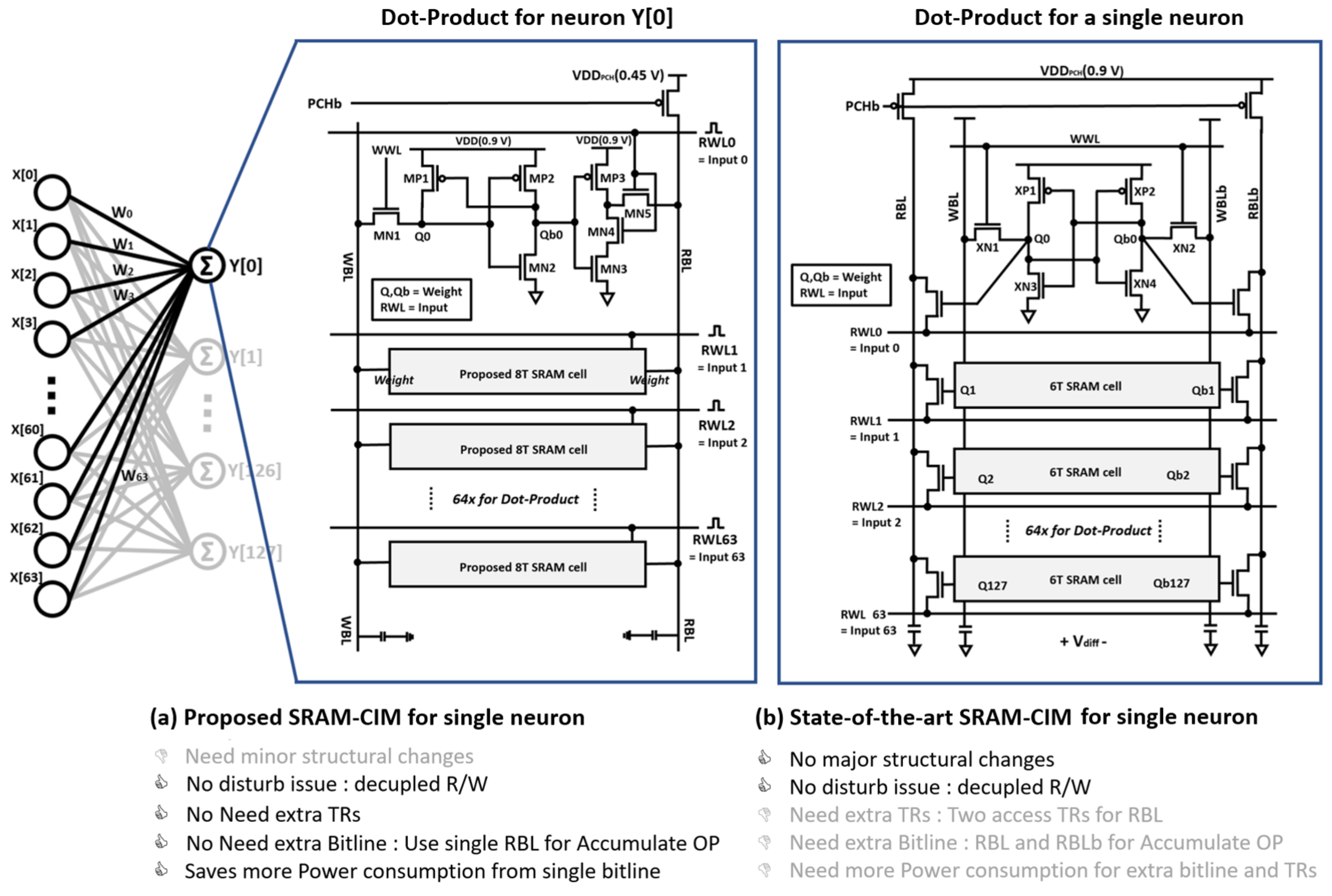
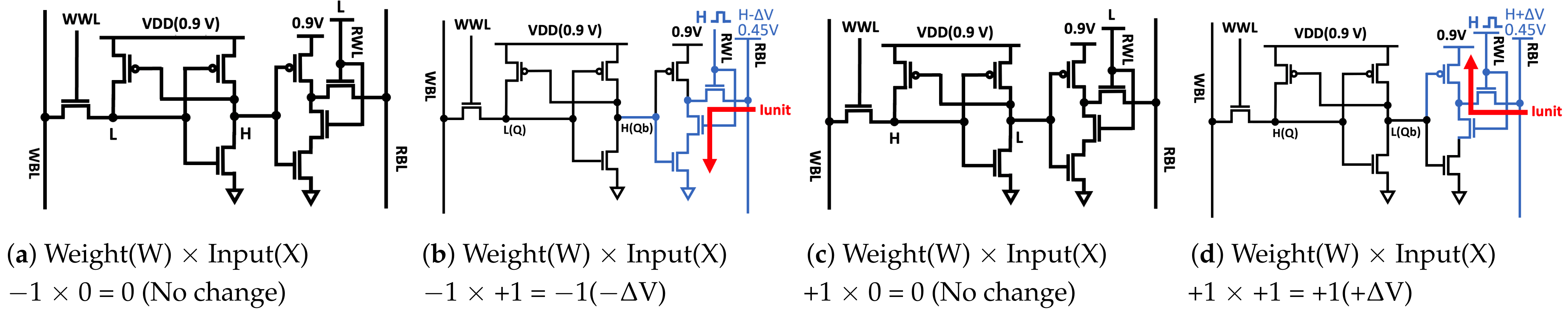
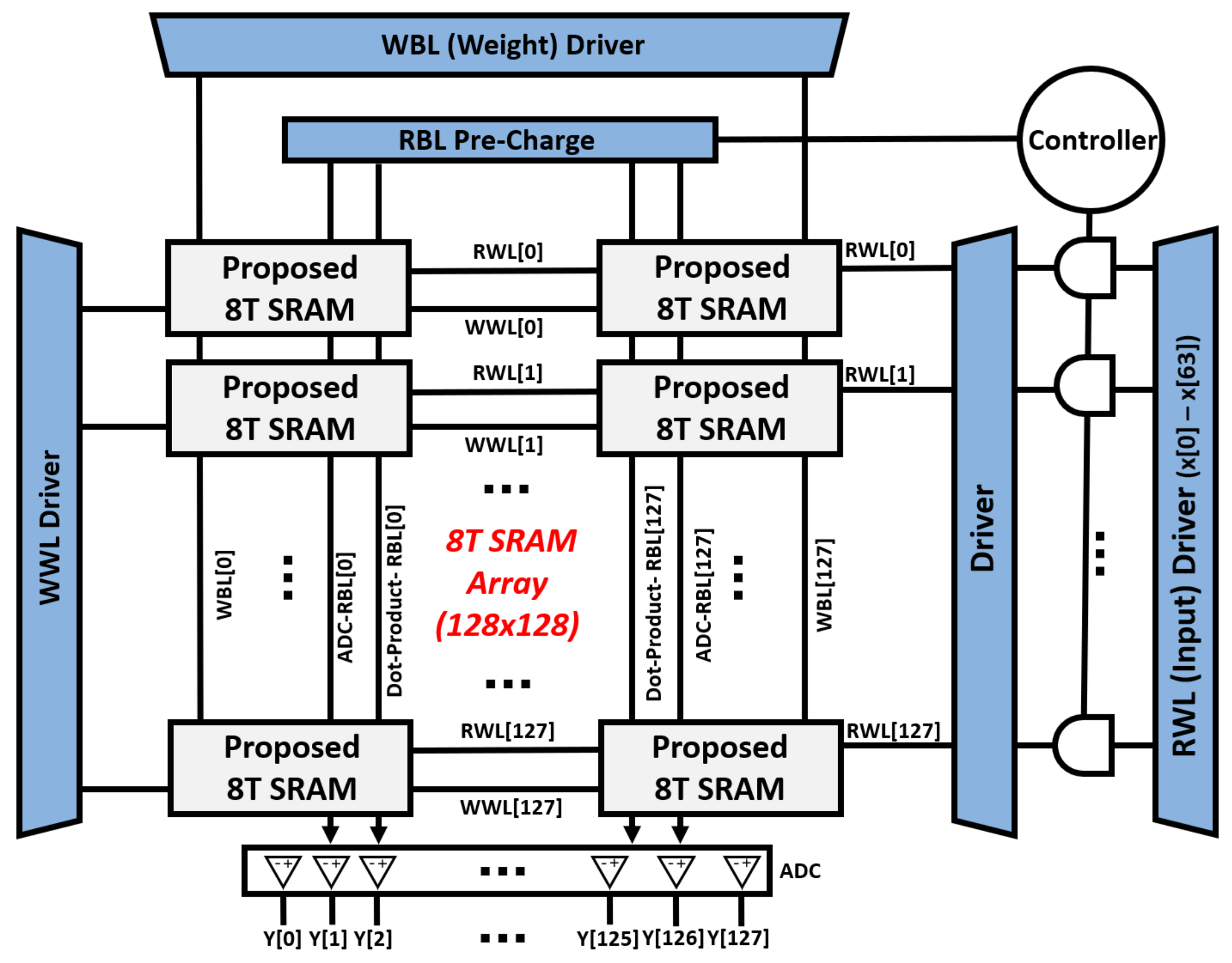
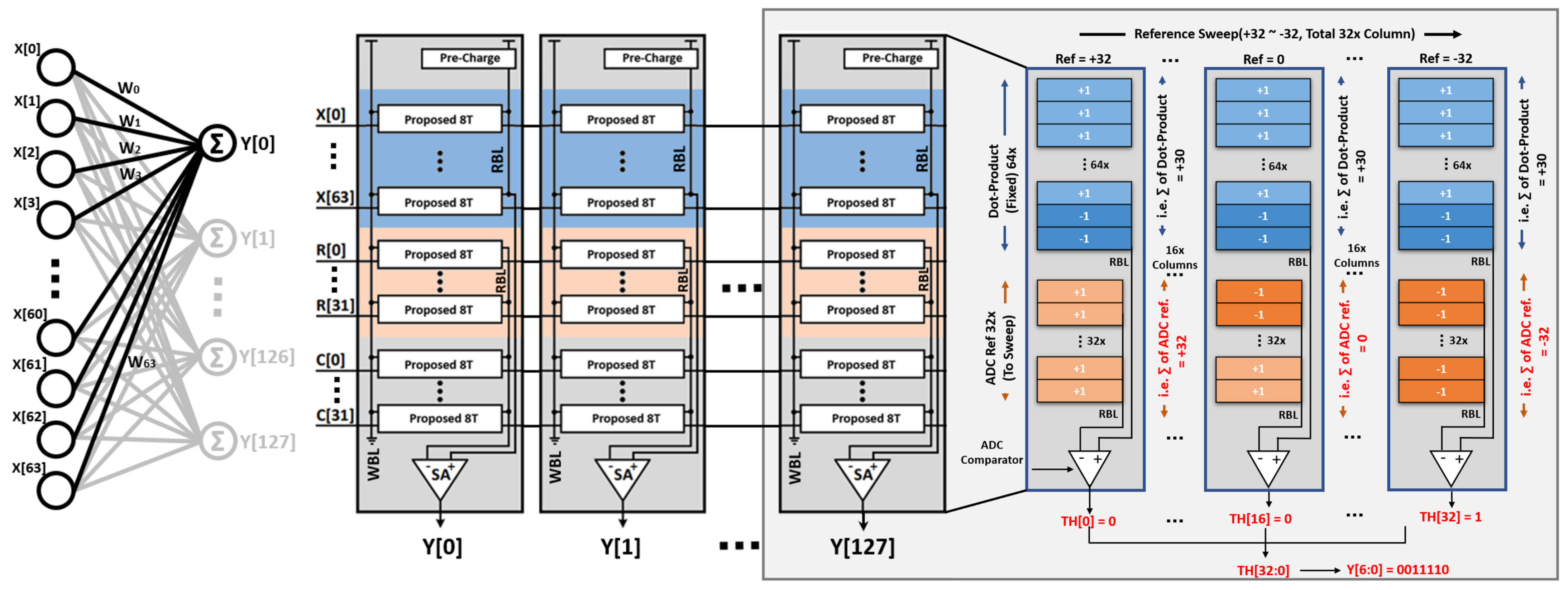
2. Proposed Compute-in-Memory Design
Figure 1a shows the column for single neuron calculation using the newly proposed SRAM cell, and Figure 1b shows the state-of-the-art SRAM-CIM for single neuron. The newly proposed SRAM cell has an independent structure, as the write unit and the read unit are completely isolated. BNN multiplication can be performed in the read unit, and weight values for BNN can be stored in Q and Qb with the write unit. We have completely solved the disturbing issue between reading and writing by making this completely independent of reading and writing, and the read unit can support CIM calculation without any extra transistors.
Figure 1.
Comparison of (a) proposed 8T-based SRAM-CIM for 64× dot-product cell array and (b) the-state-of-the-art 6T-based SRAM-CIM [18].
In addition, the stacked structure of our read unit significantly reduces leakage power for BNN calculation. Furthermore, by using a single-read bit line structure, unlike the conventional SRAM cell, unnecessary power consumption is diminished. Furthermore, the proposed new SRAM cell provides a high yield in the low-threshold operating region, and can support a stable cache in Negative Temperature Coefficient (NTC)-based systems. Our proposed new single-ended SRAM bit cell structure has the disadvantage of having to design a special sense amplifier due to the single-read bit line (RBL), but it has many advantages in terms of delay and power consumption.
Table 2 shows the four possible states of BNN calculation according to our proposed cell, and the detailed operation of the vector-matrix multiplication is shown in Figure 2. For BNN calculation, we must allocate 0 or 1 as a binary input, which can be implemented by applying a positive pulse through RWL. The 0 state of the input is the basic low state, and input 1 can be expressed by applying a positive short pulse. The weight value can be stored as −1 (i.e., Q = L, Qb = H) or +1 (Q = H, Qb = L) through the write unit of SRAM cell. When RWL is L, the transistor of the read unit connected to RWL is turned off, so the output of RBL remains the same as the precharged state (0.45 V). Conversely, when RWL is H, the transistor of the read unit connected to the RWL is turned on and the RBL is discharged or charged. Due to the stacked structure of the read unit, a considerable amount of power consumption can be reduced for discharging operations. The discharging and charging status of RBL is controlled through the weight value stored in Qb and the inverter of the read unit.
Table 2.
Possible four states of the proposed SRAM-CIM with binary input/weight combinations.
Figure 2.
Charging or discharging operation for possible four states with binary input/weight combinations of the proposed SRAM-CIM.
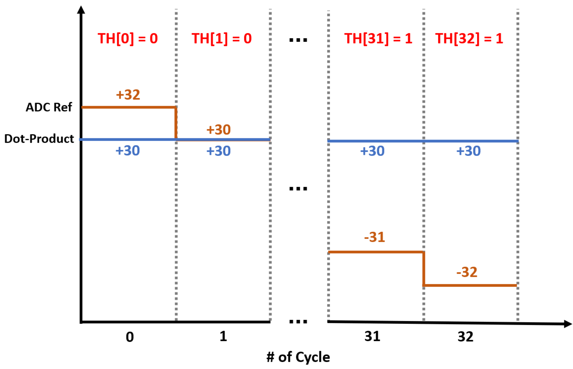
3. A Column-Based Neuron Design for BNN
Figure 3 shows the diagram of the proposed SRAM-CIM for the 16 K fully connected Binary Neural Network (BNN). Our column-based neuron contains a total of 128 bit cells in a single column, including 64 cells for dot-product, 32 cells for ADC reference and 32 cells for ADC calibration. The analog result of dot-product is quantized using comparator ADC with ADC reference cells, and the sense amplifier at the bottom is used to sequentially quantize the dot product. Comparators are similar to OP amps, and typically used in applications where various signal levels are compared to a fixed voltage reference. Due to this characteristic, most comparators are used as 1-bit Analog-to-Digital Converter (ADC), and we quantized our analog sum of the dot-product results using this principle.
Figure 3.
(left) A schematic diagram of the proposed column-based SRAM-CIM corresponding to the fully-connected layer. (64× input and 128× neurons) (right) Structure of column ADC (64× input for 7-bit output).
For example, if we have 64× dot-products and 32× ADC reference cells, according to Equation (1) of the , where N is the number of output bits, we need cycles for ADC, as shown in Figure 3 right). When the weight values are stored in the dot-product cells, as shown in Figure 3 right, we can calculate the sum of 64x dot-product values according to the RBL operation (i.e., In Figure 3, the sum of dot-product results is +30) through the charge or discharge operation of the RBL. In 33 cycles for ADC operation, where each cycle is an ADC reference, cell values can be swept from −32 to +32 depending on step size 2. As shown in Figure 4, the swept ADC reference value (−32∼+32) and the sum of the dot-product results (+30) is compared according to the comparator ADC basic operation method; if the dot-product sum (+30) is less than the ADC reference value, it is quantized as 0. If it is larger or equal to the ADC reference value, it is quantized as 1. After 33 cycles, 1 bit results of each cycle TH[0], TH[1], …, TH[32] are concatenated to obtain 33 bits of TH[32:0] quantized value. The generated 33 bits thermometer value is subsequently converted into a 7-bits binary output value for a single neuron by using the one-hot coding method [22].
Figure 4.
Comparison method for ADC operation (64× input for 7 bit output).
Figure 5 shows the overall CIM architecture using the proposed SRAM cell. 128× bit cells for 64× (x[0]− x[63]) inputs are connected vertically, and each column represents each neuron. This structure aims towards 16 K SRAM-CIM, and the test chip to be considered in the next paper will be fabricated as follows. This structure is designed by separating the RBL for dot-product cell and RBL for ADC-ref for ADC comparator for each column, and WBL is designed to be used across all cells. In the case of a write operation to store the weight value, a signal is applied to the WBL through the WBL driver controlled by the WWL driver. In other words, the WWL driver selectively controls the row for writing, and applies a signal to the selected row through the WBL driver. Unlike the state-of-the-art structure, we use a single bit line (WBL, RBL) structure, so there is no disturbing issue of R/W, resulting in a lot of improvement in stability. Furthermore, there is no need for an extra transistor for CIM calculation due to the independence of the read bitline. Therefore, the proposed structure shows improved results in terms of delay and power consumption, as well as in the stability of CIM. To reduce unnecessary power consumption in the pre-charge, the pre-charge driver pre-charges only when input is applied to the input driver through the AND gate and controller.
Figure 5.
Overall architecture of the proposed 16K SRAM-CIM (64× input and 128× neurons).
4. Performance Evaluation and Analysis
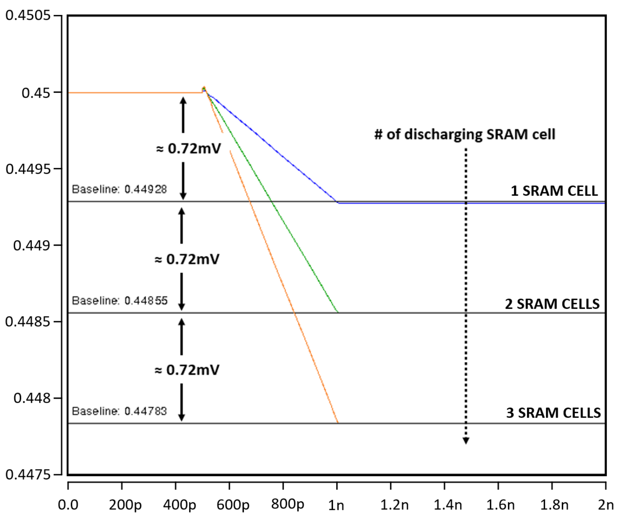
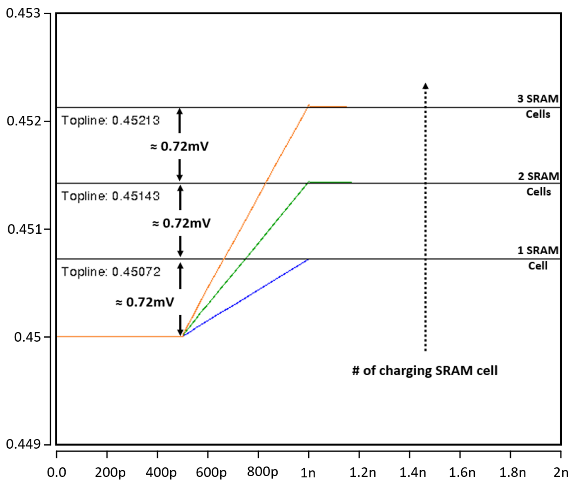
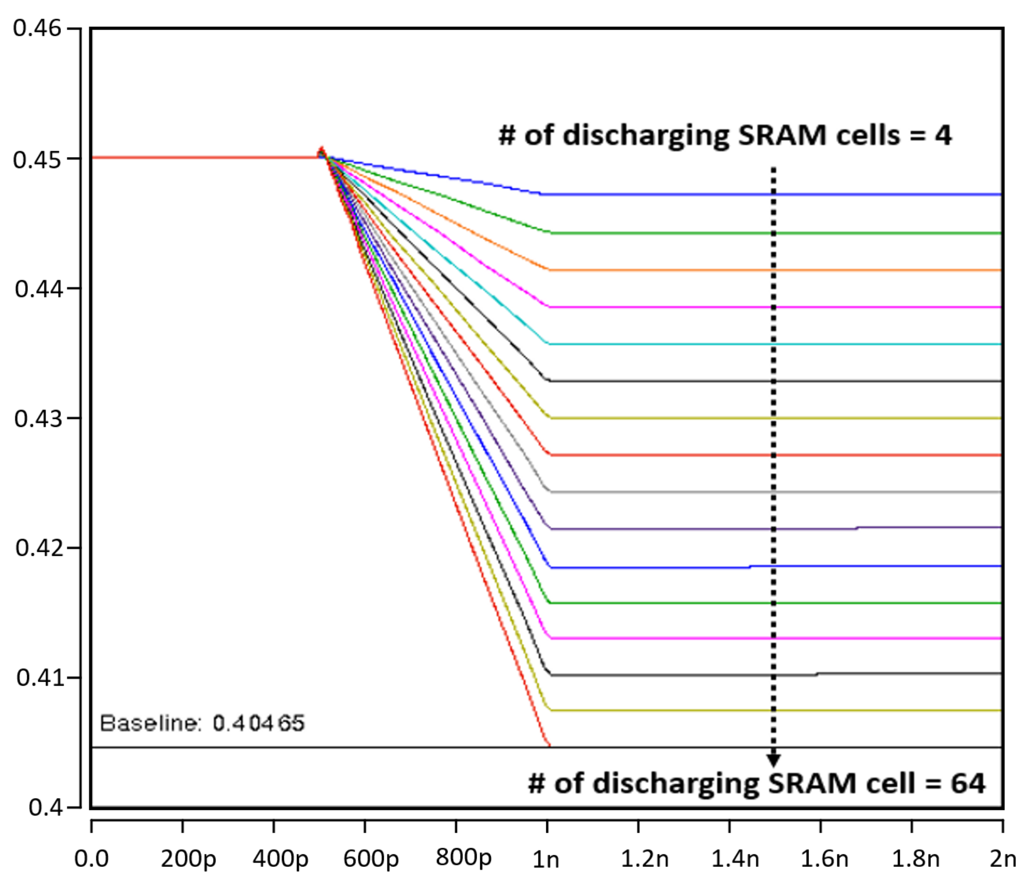
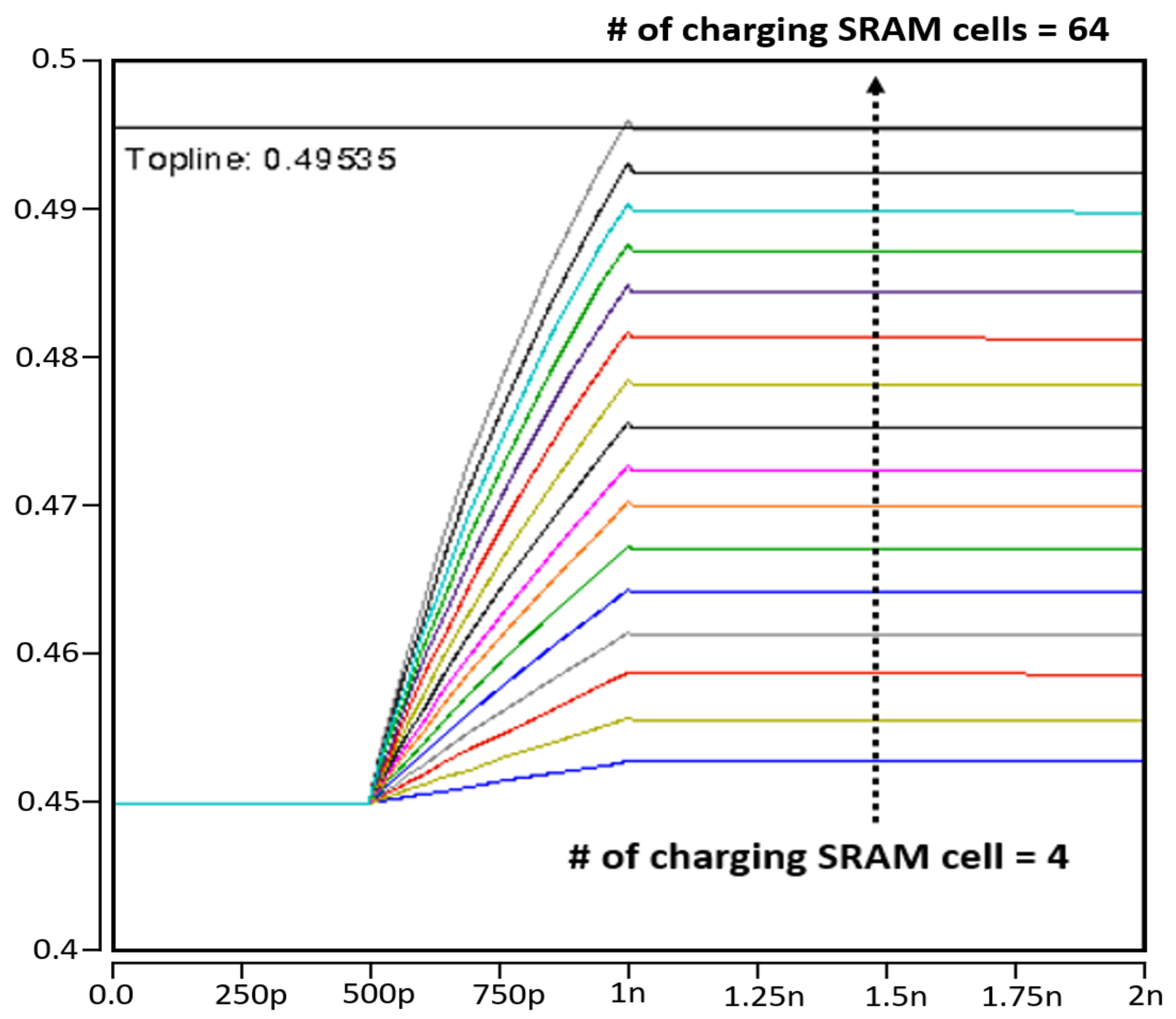
4.1. Proposed Compute-in-Memory Design
For reliable implementation, we used the same transistor size, capacitor size, voltage source, temperature and test circuit as in the proposed CIM and the conventional CIM, and all the conditions were identical. We used FreePDK 45 nm technology for verification of the proposed structure and simulated it with Synopsys Hspice and Cosmoscope.
In our column-based neuron design, the charging or discharge level in the RBL of a single SRAM cell is set to 0.72 mV to ensure the linearity of the accumulated work, which increases or decreases according to the number of SRAM cells (i.e., if two SRAM cells are discharged, the RBL discharge level becomes 0.72 × 2 = 1.44 mV). In other words, in our column-based design, the cell’s charging or discharging result is accumulated in the RBL to sum the multiplied (input × weight) result in each cell into one neuron value. We applied 0.9 V as VDD of all bit cells to maintain the linearity of the result and reduce leakage current, and set the pre-charge voltage to 0.45 V, which is half of 0.9 V for charge or discharge of RBL. Therefore, according to our multiplication method described in Table 2, when +1 ×−1 = −1, RBL is discharged from 0.45 V to 0 V, and when +1 × +1 = +1, RBL is charged from 0.45 V to 0.9 V, respectively. The charged or discharged range can be calculated with Equation (2).
Tau () represents the charge and discharge delay of RBL, which can be controlled by the pulse width of RWL. We evaluated the maximum stacking range on RBL when the 64× input results are stacked as −64 or +64. Figure 6, Figure 7, Figure 8, Figure 9, Figure 10 and Figure 11 described that each bit cell is stacked while maintaining linearity and single bit cell range ( 0.72 mV).
Figure 6.
Discharging range with a single SRAM bit cell (0.72 mV).
Figure 7.
Charging range with a single SRAM bit cell (0.72 mV).
Figure 8.
Comparison of read bitline (RBL) discharging range with a different number of SRAM bitcells (1 cell–3 cells).
Figure 9.
Comparison of read bitline (RBL) charging range with a different number of SRAM bitcells (1 cell–3 cells).
Figure 10.
Comparison of read bitline (RBL) discharging range with different number of SRAM bitcells (4 cells–64 cells).
Figure 11.
Comparison of read bitline (RBL) charging range with different number of SRAM bitcells (4 cells–64 cells).
Our single bit line CIM technology is more effective in maintaining and reducing power consumption than the conventional method, as there is only one bitline. The decoupled reading and writing of our new bitcell offers better low-power consumption due to the stacking of device in the read unit, as well as achieving better readability and writability. Table 3 shows the comparison results of dynamic power consumption of traditional SRAM-CIM and proposed SRAM-CIM. As described in Figure 1, our proposed CIM structure does not require extra transistors and bitlines for multiplication, so a significant amount of power consumption has been saved.
Table 3.
Comparison of dynamic power consumption with state-of-the-art 8T SRAM-based CIM [18] for a possible four states with binary input/weight combinations.
We reduced power consumption by 92.34% in operation for bitline charging and 98.71% in operation for discharging, respectively. In the operation for −1 × 0 and +1 × 0 calculations, the power consumption has been reduced by up to 99.96% compared to the state-of-the-art SRAM-CIM.
Figure 10 and Figure 11 show the accumulation results of multiplication results. Since our CIM has a total of 64× inputs from X[0] to X[63], the maximum value of the sum of binary multiplication results can be +64 or −64. The discharging or charging range of a single cell is 0.72 mV, which can indicate −1 or +1. Therefore, the sum of the multiplication results of 64× cells is 0.00072 V (0.72 mV) × 64 = 0.046 V, which can be charged or discharged at the reference point (0.45 V) for representing the +64 or −64. In other words, a value of −64 can be expressed as 0.45 V − 0.046 V = 0.404 V, and a value of +64 can be expressed as 0.45 V + 0.046 V = 0.495 V. The results are simulated in detail in Figure 10 and Figure 11, and it can be confirmed that our results maintain the linearity of the accumulated work.
4.2. Proposed SRAM Bit Cell Design
In SRAM bit cell power consumption, switching power consumption occupies a larger portion than other power consumption, which cannot be ignored. In order to reduce this switching power consumption, We proposed a new SRAM bitcell that eliminates the switching of weak inverters [23]. In addition, as described in the previous section, our bitcell solves the disturbing issue between reading and writing as read and write operations are completely separated as shown in Figure 1. Decoupled R/W operation is very effective at reducing power consumption and is also very advanced in delaying CIM calculation. Unlike the conventional bitcell, our access transistors MN1 and MN5 are separate for read and write operations. In other words, the MN1 transistor is used for the operation for writing and the MN5 transistor is used for the operation for reading. We set the size of driver transistors MN2 and MN3 to the strongest for the read and write stability of the cell, and set the load transistor to the smallest. The access transistor is set to a smaller size than the driver transistor, in consideration of the bit line voltage. Table 4 shows the transistor size and the ratio for bit cell configuration.
Table 4.
Transistor size and ratio for bit cell configuration.
Table 5 shows that our proposed bitcell improves the write operation speed by up to 91.2% due to the optimized transistor size, ratio and the structural characteristics of the writing part. This write delay supports a fast storage capability for storing weight values in the CIM. In addition to the low power and fast writing ability, our proposed bitcell supports high stability, as analyzed in the next section.
Table 5.
Delay comparison of proposed 8T SRAM bit cell with state-of-the-art 8T SRAM bit cell [23].
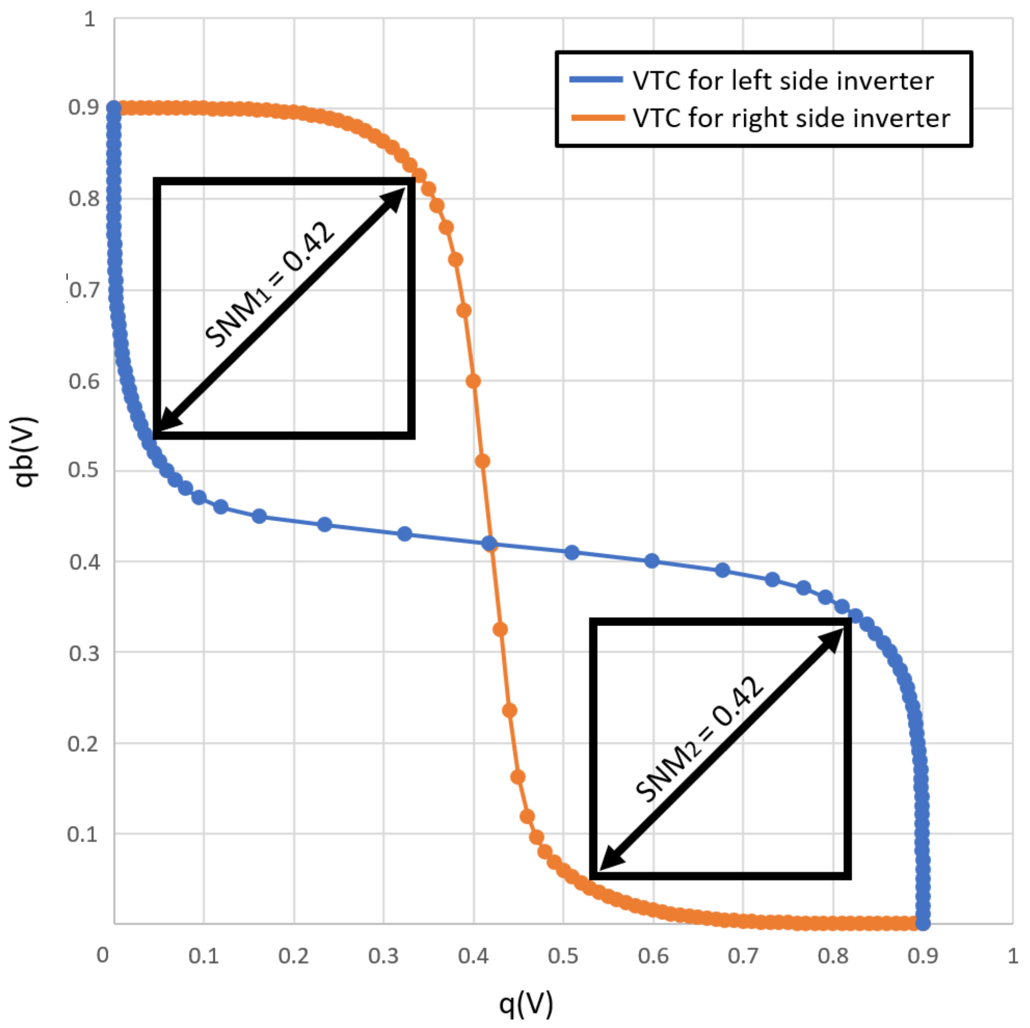
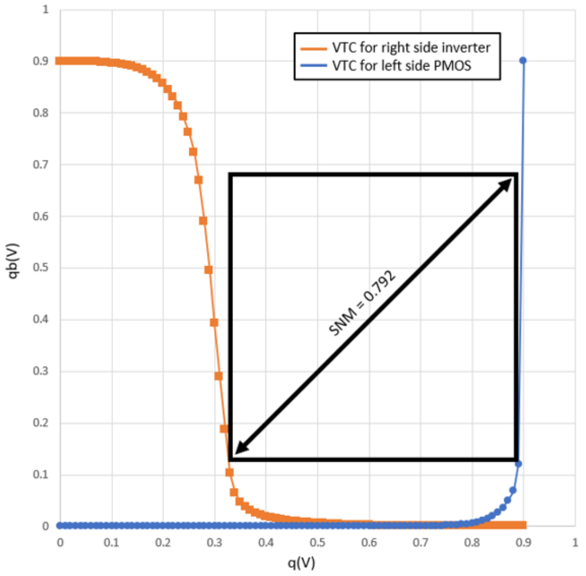
4.2.1. Hold Static Noise Margin (SNM)
Hold Static Noise Margin (SNM) is a standard for evaluating the stability of a cell against noise when data are stored. In other words, Hold SNM shows the noise tolerance that prevents the cell from losing ‘stored’ bits. Therefore, it is necessary to secure the SNM that can be represented in a square shape, as shown in Figure 12 and Figure 13 to the maximum for stable cell data storage.
Figure 12.
Hold Static Noise Margin (SNM) of the Proposed 8T SRAM bit cell.
Figure 13.
Hold Static Noise Margin (SNM) of the state-of-the-art 8T SRAM bit cell.
To plot the SNM, we firsty plot the Vin and Vout DC characteristics. By swapping the X/Y axis of either Vin or Vout, we can create the largest square, which fits the continuous DC characteristic representing the SNM. Compared to the state-of-the-art 8T SRAM bitcell, our proposed 8T SRAM bitcell not only supports low power consumption and high-throughput, it also shows an 88% improvement in Hold SNM. This means that our proposed 8T SRAM has a lower risk of lost ‘memorized’ bits of memory than traditional SRAM. We have focused on maintaining the maximum SNM in the SRAM structure and providing the maximum low-power and high-throughput effect for AI calculation.
Furthermore, because of the decoupled reading unit from an internal node of latch, proposed our SRAM has no feedback from the reading unit, resulting in its being read static noise margin (RSNM)-free.
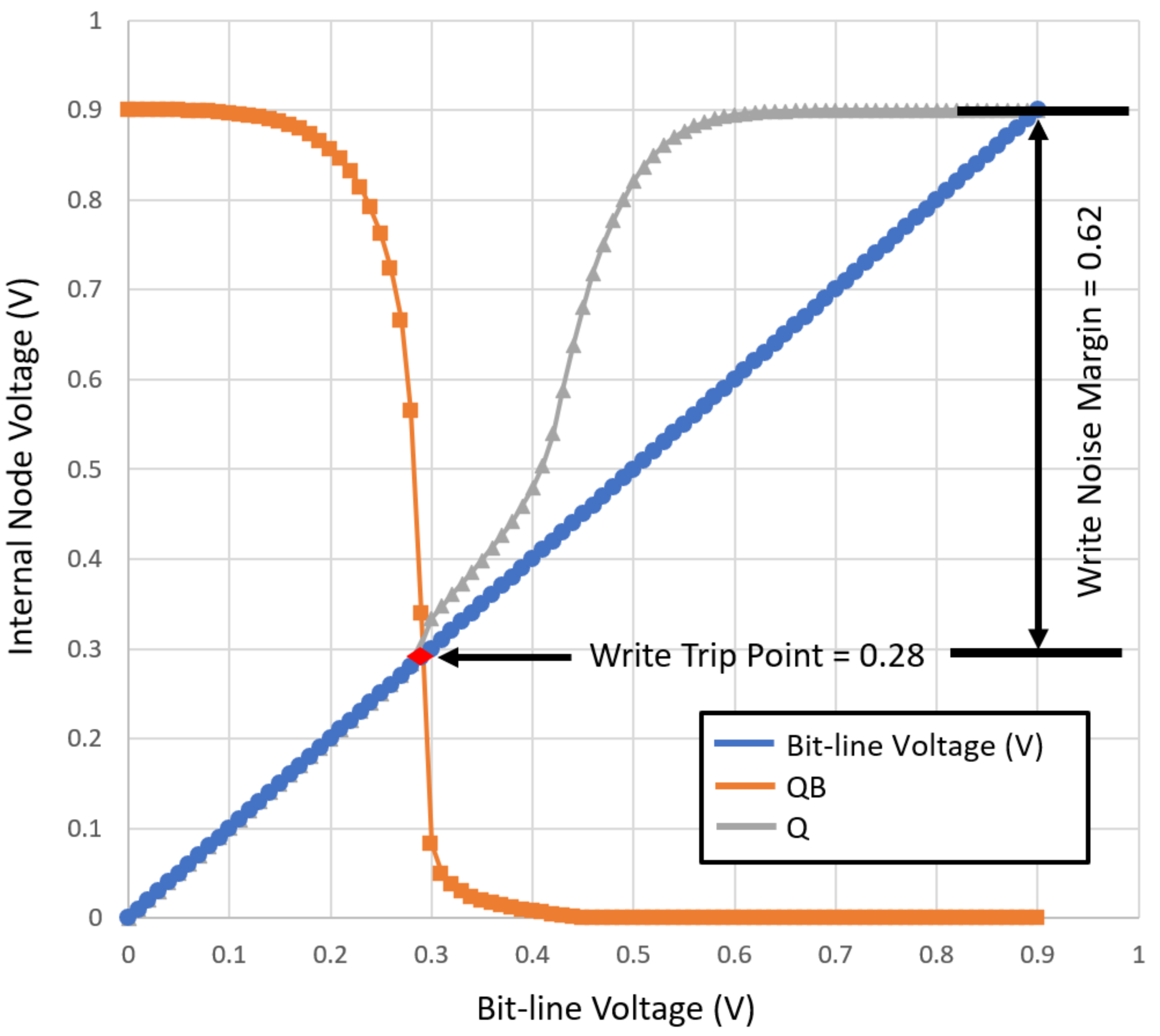
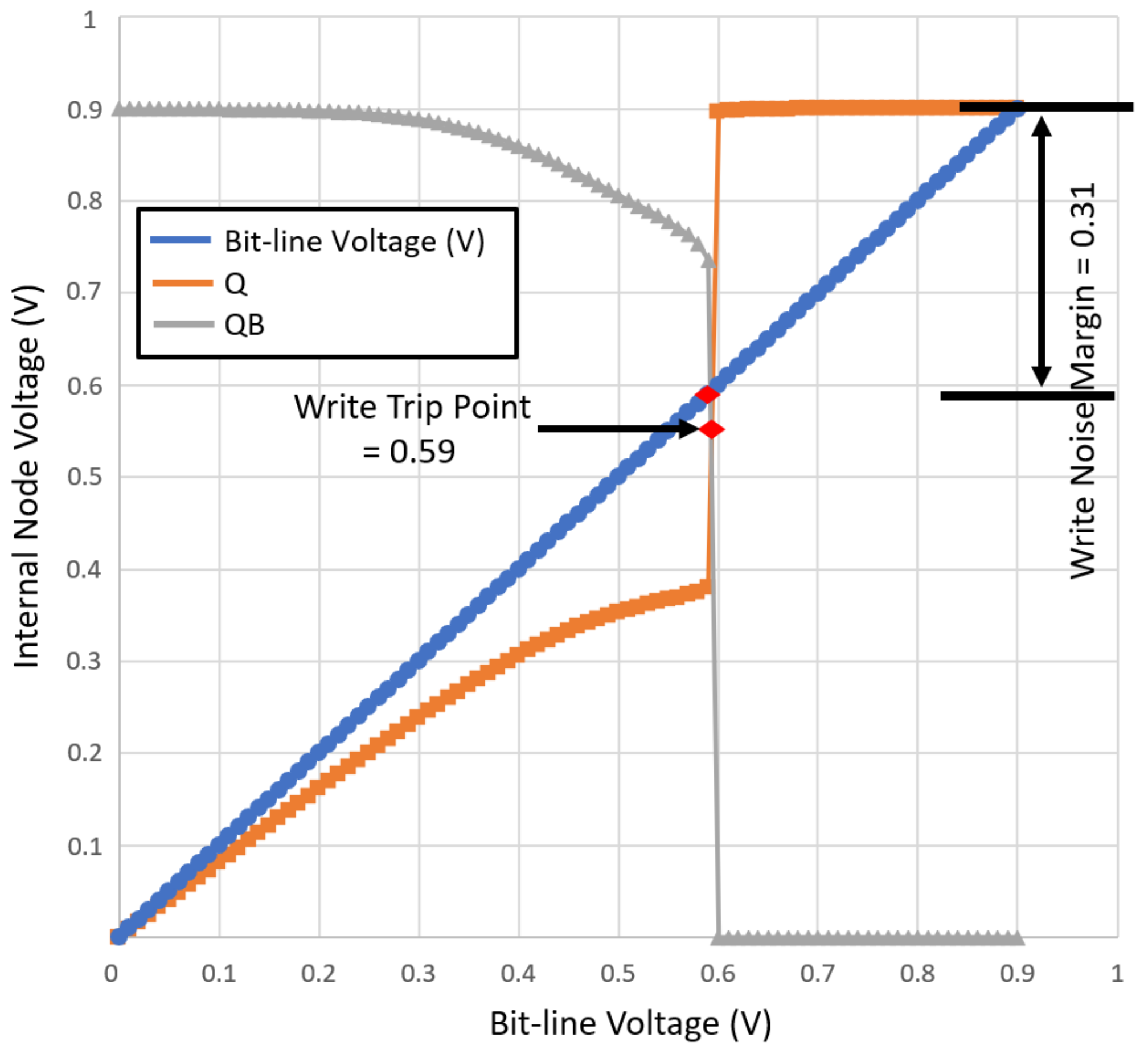
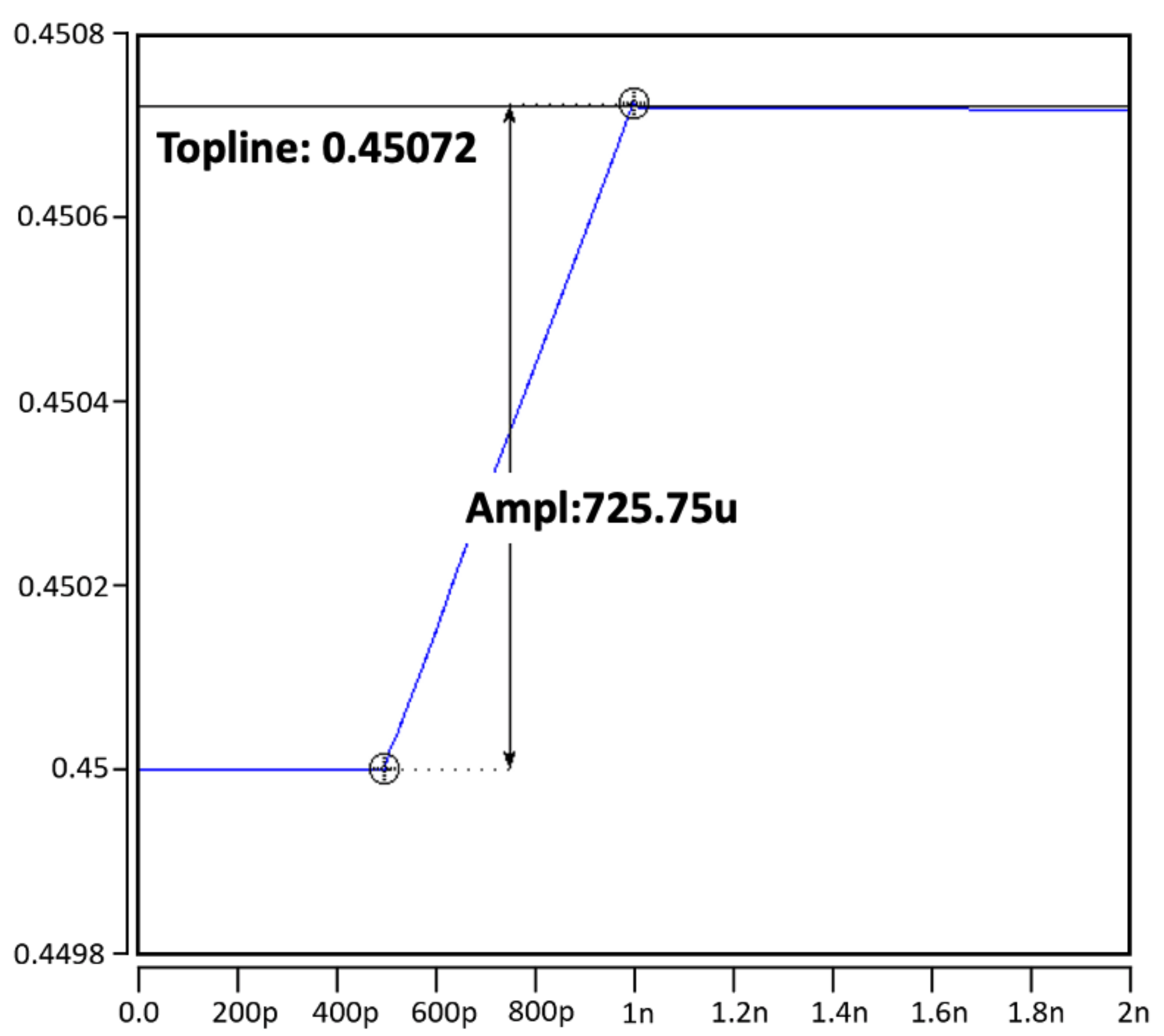
4.2.2. Write Noise Margin (WNM)
Write ability is measured using Write Trip Point (WTP) analysis. On increasing the BL voltage 0 to Vdd, the BL voltage where Q and Qb flip is WTP. As can be seen in Figure 14 and Figure 15, the write trip point of the proposed and traditional SRAM cells are 0.28 V and 0.59 V, which make the write noise margin (WNM) 0.62 and 0.31, respectively. Therefore, the proposed bitcell is more stable for write operation.
Figure 14.
Write Noise Margin (WNM) of the proposed 8T SRAM bit cell.
Figure 15.
Write Noise Margin (WNM) of the state-of-the-art 8T SRAM bit cell.
5. Conclusions
In this paper, we propose a novel 8T SRAM-based ultra-low-power compute-in-memory (CIM) design. To compute the vector-matrix multiplication of the binary weight and input, we use dot-products based on the voltage-mode accumulation. By using the decoupled read, write unit, and single bitline (RBL), the disturbing issue between read and write operation has been eliminated. For the simulation, each column including 128× bit cells consist of 64× cells for dot-product and 32× cells for ADC reference, and additionally, 32× cells for offset calibration have been added. Our row-by-row ADC can support 1–7 bits output for the quantized single neuron value. Based on the simulation results, the proposed SRAM-CIM saves up to 99.96% of total power consumption for computing the vector-matrix multiplication of the binary weight and input compared with the state-of-the-art SRAM-CIM.
Author Contributions
Conceptualization, Data curation, Formal analysis, Investigation, Methodology, Validation, Y.K.; Writing—original draft, Writing—review and editing, Y.K., S.L., N.Y. and K.K.C.; Supervision, Funding acquisition, Project administration, K.K.C. All authors read and agreed to the published version of the manuscript.
Funding
This work is supported by the Industrial Core Technology Development Program of MOTIE/KEIT, KOREA. (#10083639, Development of Camera-based Real-time Artificial Intelligence System for Detecting Driving Environment & Recognizing Objects on Road Simultaneously).
Institutional Review Board Statement
Not applicable.
Informed Consent Statement
Not applicable.
Acknowledgments
We thank our colleagues from KETI and KEIT who provided insight and expertise that greatly assisted the research and greatly improved the manuscript.
Conflicts of Interest
The authors declare no conflict of interest.
Abbreviations
The following abbreviations are used in this manuscript:
| SRAM | Static Random-Access Memory |
| CIM | Compute-In-Memory |
| ADC | Analog to Digital Converter |
| BNN | Binary Neural Networks |
| SNM | Static Noise Margin |
| WNM | Write Noise Margin |
| WTP | Write Trip Point |
References
- Deng, L.; Li, G.; Han, S.; Shi, L.; Xie, Y. Model Compression and Hardware Acceleration for Neural Networks: A Comprehensive Survey. Proc. IEEE 2020, 108, 485–532. [Google Scholar] [CrossRef]
- Mühlroth, C.; Grottke, M. Artificial Intelligence in Innovation: How to Spot Emerging Trends and Technologies. IEEE Trans. Eng. Manag. 2020, 1–18. [Google Scholar] [CrossRef]
- Biswas, A.; Chandrakasan, A. Conv-RAM: An energy-efficient SRAM with embedded convolution computation for low-power CNN-based machine learning applications. In Proceedings of the 2018 IEEE International Solid—State Circuits Conference—(ISSCC), San Francisco, CA, USA, 11–15 February 2018; pp. 488–490. [Google Scholar]
- Jiang, Z.; Yin, S.; Seok, M.; Seo, J.S. XNOR-SRAM: In-Memory Computing SRAM Macro for Binary/Ternary Deep Neural Networks. IEEE J. Solid-State Circuits 2020, 55, 1733–1743. [Google Scholar] [CrossRef]
- Yang, Z.; Wei, L. Logic Circuit and Memory Design for In-Memory Computing Applications using Bipolar RRAMs. In Proceedings of the 2019 IEEE International Symposium on Circuits and Systems (ISCAS), Sapporo, Japan, 26–29 May 2019; pp. 1–5. [Google Scholar] [CrossRef]
- Jiang, Z.; Yin, S.; Seo, J.S.; Seok, M. C3SRAM: In-Memory-Computing SRAM Macro Based on Capacitive-Coupling Computing. IEEE Solid-State Circuits Lett. 2019, 2, 131–134. [Google Scholar] [CrossRef]
- Yan, B.; Li, B.; Qiao, X.; Xue, C.X.; Chang, M.F.; Chen, Y.; Li, H.H. Resistive Memory-Based In-Memory Computing: From Device and Large-Scale Integration System Perspectives. Adv. Intell. Syst. 2019, 1, 1900068. [Google Scholar] [CrossRef] [Green Version]
- Wang, W.; Lin, B. Trained Biased Number Representation for ReRAM-Based Neural Network Accelerators. J. Emerg. Technol. Comput. Syst. 2019, 15, 1–17. [Google Scholar] [CrossRef]
- Huang, S.; Ankit, A.; Silveira, P.; Antunes, R.; Chalamalasetti, S.R.; Hajj, I.E.; Kim, D.E.; Aguiar, G.; Bruel, P.; Serebryakov, S.; et al. Mixed Precision Quantization for ReRAM-based DNN Inference Accelerators. In Proceedings of the 2021 26th Asia and South Pacific Design Automation Conference (ASP-DAC), Tokyo, Japan, 18–21 January 2021; pp. 372–377. [Google Scholar]
- Yu, S. Resistive Random Access Memory (RRAM). Synth. Lect. Emerg. Eng. Technol. 2016, 2, 1–79. [Google Scholar] [CrossRef]
- Suri, M.; Gupta, A.; Parmar, V.; Lee, K.H. Performance Enhancement of Edge-AI-Inference Using Commodity MRAM: IoT Case Study. In Proceedings of the 2019 IEEE 11th International Memory Workshop (IMW), Monterey, CA, USA, 12–15 May 2019; pp. 1–4. [Google Scholar] [CrossRef]
- Gao, S.; Chen, B.; Qu, Y.; Zhao, Y. MRAM Acceleration Core for Vector Matrix Multiplication and XNOR-Binarized Neural Network Inference. In Proceedings of the 2020 International Symposium on VLSI Technology, Systems and Applications (VLSI-TSA), Hsinchu, Taiwan, 10–13 August 2020; pp. 153–154. [Google Scholar] [CrossRef]
- Xu, T.C.; Leppänen, V. Analysing emerging memory technologies for big data and signal processing applications. In Proceedings of the 2015 Fifth International Conference on Digital Information Processing and Communications (ICDIPC), Sierre, Switzerland, 7–9 October 2015; pp. 104–109. [Google Scholar] [CrossRef]
- Sun, X.; Liu, R.; Peng, X.; Yu, S. Computing-in-Memory with SRAM and RRAM for Binary Neural Networks. In Proceedings of the 2018 14th IEEE International Conference on Solid-State and Integrated Circuit Technology (ICSICT), Qingdao, China, 31 October–3 November 2018; pp. 1–4. [Google Scholar] [CrossRef]
- Zhang, J.; Wang, Z.; Verma, N. A machine-learning classifier implemented in a standard 6T SRAM array. In Proceedings of the 2016 IEEE Symposium on VLSI Circuits (VLSI-Circuits), Honolulu, HI, USA, 15–17 June 2016; pp. 1–2. [Google Scholar] [CrossRef]
- Si, X.; Khwa, W.S.; Chen, J.J.; Li, J.F.; Sun, X.; Liu, R.; Yu, S.; Yamauchi, H.; Li, Q.; Chang, M.F. A Dual-Split 6T SRAM-Based Computing-in-Memory Unit-Macro With Fully Parallel Product-Sum Operation for Binarized DNN Edge Processors. IEEE Trans. Circuits Syst. I Regul. Pap. 2019, 66, 4172–4185. [Google Scholar] [CrossRef]
- Kim, H.; Chen, Q.; Kim, B. A 16K SRAM-Based Mixed-Signal In-Memory Computing Macro Featuring Voltage-Mode Accumulator and Row-by-Row ADC. In Proceedings of the 2019 IEEE Asian Solid-State Circuits Conference (A-SSCC), Macao, China, 4–6 November 2019; pp. 35–36. [Google Scholar] [CrossRef]
- Yu, C.; Yoo, T.; Kim, T.T.; Tshun Chuan, K.C.; Kim, B. A 16K Current-Based 8T SRAM Compute-In-Memory Macro with Decoupled Read/Write and 1-5bit Column ADC. In Proceedings of the 2020 IEEE Custom Integrated Circuits Conference (CICC), Boston, MA, USA, 22–25 March 2020; pp. 1–4. [Google Scholar] [CrossRef]
- Maddah, R.; Melhem, R.; Cho, S. RDIS: Tolerating Many Stuck-At Faults in Resistive Memory. IEEE Trans. Comput. 2015, 64, 847–861. [Google Scholar] [CrossRef]
- Dong, X.; Wu, X.; Sun, G.; Xie, Y.; Li, H.; Chen, Y. Circuit and microarchitecture evaluation of 3D stacking magnetic RAM (MRAM) as a universal memory replacement. In Proceedings of the 2008 45th ACM/IEEE Design Automation Conference, Anaheim, CA, USA, 8–13 June 2008; pp. 554–559. [Google Scholar]
- Klostermann, U.; Angerbauer, M.; Gruning, U.; Kreupl, F.; Ruhrig, M.; Dahmani, F.; Kund, M.; Muller, G. A Perpendicular Spin Torque Switching based MRAM for the 28 nm Technology Node. In Proceedings of the 2007 IEEE International Electron Devices Meeting, Washington, DC, USA, 10–12 December 2007; pp. 187–190. [Google Scholar] [CrossRef]
- Raajitha, K.; Meenakshi, K.; Rao, Y.M. Design of Thermometer Coding and One-Hot Coding. In Proceedings of the 2021 Third International Conference on Intelligent Communication Technologies and Virtual Mobile Networks (ICICV), Tirunelveli, India, 4–6 February 2021; pp. 601–609. [Google Scholar] [CrossRef]
- Kim, Y.; Patel, S.; Kim, H.; Yadav, N.; Choi, K.K. Ultra-Low Power and High-Throughput SRAM Design to Enhance AI Computing Ability in Autonomous Vehicles. Electronics 2021, 10, 256. [Google Scholar] [CrossRef]
Publisher’s Note: MDPI stays neutral with regard to jurisdictional claims in published maps and institutional affiliations. |
© 2021 by the authors. Licensee MDPI, Basel, Switzerland. This article is an open access article distributed under the terms and conditions of the Creative Commons Attribution (CC BY) license (https://creativecommons.org/licenses/by/4.0/).