Abstract
This paper proposes a 6H-materials silicon carbide (SiC)/gallium nitride (GaN) heterogeneous p-n structure to replace the GaN homogenous p-n junction to manufacture an impact-ionization-avalanche-transit-time (IMPATT) diode, and the performance of this 6H-SiC/GaN heterojunction single-drift-region (SDR) IMPATT diode is simulated at frequencies above 100 GHz. The performance parameters of the studied device were simulated and compared with the conventional GaN p-n IMPATT diode. The results show that the p-SiC/n-GaN IMPATT performance is significantly improved, and this is reflected in the enhanced characteristics in terms of operating frequency, rf power, and dc-rf conversion efficiency by the two mechanisms. One such characteristic that the new structure has an excessive avalanche injection of electrons in the p-type SiC region owing to the ionization characteristics of the SiC material, while another is a lower electric field distribution in the drift region, which can induce a higher electron velocity and larger current in the structure. The work provides a reference to obtain a deeper understanding of the mechanism and design of IMPATT devices based on wide-bandgap semiconductor materials.
1. Introduction
Among all the options of microwave and terahertz wave solid-state source devices, the impact-ionization-avalanche-transit-time (IMPATT) diode is one of the most promising candidates due to its high rf power and dc-rf conversion efficiency [1,2]. The IMPATT performance is determined by the structural design and material characteristics. For the material selection of IMPATT devices, the third-generation wide-bandgap semiconductor materials silicon carbide (SiC) and gallium nitride (GaN) have many optional advantages, including their high electron speed and breakdown voltage, which have received widespread attention [3,4]. Conventional IMPATT diodes have a high-low doped p-n junction (high-low structure) where the avalanche process occurs mainly in the n-type region. Before the rf power of IMPATT reaches saturation, it increases with the p-region concentration [5,6]. However, the practical fabrication of p-n junction GaN structures is challenging in IMPATT devices due to the difficulty of obtaining high concentrations of p-GaN because of the very low effective hole ionization rate [7]. Eventually, the voltage and current of this negative resistance device will be reduced, impairing the diode performance severely [8]. In the previous studies, in order to avoid the use of p-type GaN and the improvement of device performance, many improvements have been made. However, their mechanism is different. Literature [9] used Schottky contacts to avoid the use of p-type GaN, but there is a problem of excessive reverse leakage compared with p-n contacts [10,11]. In the literature [12], an n-InGaN/n-GaN heterojunction was used to achieve IMPATT, forming a “Schottky-like barrier” to obtain a large reverse breakdown voltage. However, there are still several non-ideal effects at the InGaN/GaN interface in practice [13], which seriously affect the output performance of the device. As the fabrication process of growing GaN on a SiC substrate is relatively mature [14,15], it can meet the requirements of IMPATT devices. In the literature [16], a p-SiC/n-GaN double drift region IMPATT was proposed, in which electrons and holes are both involved in the transition, so the increase of the injected charge improves the device performance. Compared to the double drift structure, the single drift structure has a smaller size, a simpler structure design, and a higher power output per unit volume. In this paper, in order to improve the performance of single-drift-region (SDR) IMPATT diode as much as possible, a novel SiC/GaN heterojunction SDR IMPATT diode is proposed, where the current component is composed of electrons, and discover two mechanisms to enhance the current in the new structure. On the one hand, it is worth noting that due to the easier ionization characteristics of holes for the p-SiC material [17,18], this structure has an excessive avalanche injection of electrons from the p-type SiC region, like the double-drift structure, and the amount of injected charge is increased. In contrast, the conventional GaN-based IMPATT diode avalanche process only occurs on one side of the n-type region of the p-n junction. On the other hand, a lower electric field distribution in the drift region can be obtained, which can induce higher electron velocity and a larger current. In the new single drift structure, we not only found that the result of excessive charge injection is similar to the double drift structure IMPATT, but also that the appearance of the electric field modulation effect further improves the performance of the device. Due to the similar bandgap widths of SiC and GaN, both of which are close to 3.4 eV, the interface of the heterojunction formed by SiC and GaN has no obvious non-ideal effect on band discontinuity compared with the homogeneous p-n junction [19]. Although there is a certain interface mismatch between SiC and GaN, the technology of growing GaN on a SiC substrate is relatively mature, and the influence on the device can be minimized as much as possible [20,21]. In this work, we ignore the interface mismatch and study the ideal performance of the new structure. The results show that there are two mechanisms in the new structure. One is the electric field modulation effect in the drift region, leading to the higher electron drift velocity, and the other is the enhancement of impact ionization effect in the p-n junction, leading to the stronger electron injection. Under their joint action, the rf characteristics of the device have been significantly improved.
2. Simulation Models and Method
Figure 1 shows the diode structures and the circuit used for simulation: the WD0 region is p-type GaN and p-type 6H SiC, its thickness is 0.1 μm, and the doping concentration is 1 × 1019 cm−3. The WD1 region is an n-type doped avalanche region, its thickness is 0.2 μm, and its concentration is 1 × 1018 cm−3. The WD2 region is the drift region, its thickness is 0.3 μm, and its concentration is 5 × 1016 cm−3. The WD3 is the n-type ohmic contact region, and its concentration is 1 × 1019 cm−3, its thickness is 0.1 μm. The device structure parameters are shown in Table 1. The temperature is 300 K, and the dc bias current Jdc is 100 kA/cm2, the device cross-sectional area is 100 μm2. Figure 1c shows the rf large signal simulation circuit, using an RLC (resistance: R, inductance: L, capacitance: C) free running oscillation circuit. The ideal RLC free-running oscillation circuit consists of a capacitor C, an inductor L, and a resistor R, as well as an ideal dc current source and IMPATT diode. The diode is placed in the circuit and connected to both ends of the dc current source. The dc bias current source makes the diode work in a stable breakdown state. The LC part of the oscillation circuit is formed by the equivalent capacitance and inductance inside the IMPATT, the capacitance C and the inductance L of the external circuit. Adjust the inductance L and the capacitance C to change the oscillation frequency of the resonant circuit, and adjust the resistance R to change the oscillation amplitude. When the oscillation frequency in the LC circuit matches the operating frequency of the IMPATT diode, and the load resistance R is exactly equal to the negative resistance of the IMPATT diode, the circuit is a classic LC free-running oscillation circuit. A small excitation signal can make the entire circuit oscillate and a stable oscillation can be established. This condition implies the following equations [22]:
where Rd and RL are the diode negative resistance and the load resistance, respectively, Xd and XL are the reactance of the diode and the load, respectively, and Ud0 is the amplitude of the voltage oscillations at the diode terminals. Equations (1) and (2) determine the parameters of the load circuit for the simulation of the free-running oscillator at the given fundamental frequency.
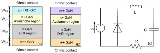
Figure 1.
Design of the Impact-Ionization-Avalanche-Transit-Time (IMPATT) diode structures and circuit: (a) 6H-SiC/GaN heterostructure p-n junction IMPATT diode, (b) GaN p-n junction IMPATT diode, (c) Free running oscillation circuit.

Table 1.
Device structure parameters.
We use the Silvaco-ATLAS platform for device simulation and the Silvaco-Mixedmode platform for comprehensive “device-circuit” simulation.
The impact ionization parameters are obtained from [17,18], where E is the electric field, while a and b are the impact ionization coefficients.
and the mobility parameters are derived from [23,24]. Different from the constant mobility model of Si-based materials, GaN materials have obvious negative differential mobility characteristics, which are also beneficial to the performance of the device [25].
since these devices are mainly used in millimeter wave and terahertz frequency bands, the tunneling effect will be more noticeable at high frequency [26,27]. So, the band to band tunneling model is also included in addition to the diffusion-drift model, impact-ionization model, and recombination model. The tunneling generation rate is obtained from [28,29], and it is given by:
where A and B are tunneling rate coefficients. Including the transition of carriers from the valence band to the conduction band and the transition from the conduction band to the valence band. The main parameters used in the above model are shown in Table 2.
Table 2.
Parameters used in the simulation.
In the simulation process, we achieve the purpose of making the circuit self-oscillate by adjusting the inductor L and resistance R, and obtain a stable periodic voltage and current waveforms after constant trial and error. Next, Fourier analysis is performed on the voltage and current waveforms in the time domain to determine the key parameters, such as rf voltage, rf current, voltage-current phase delay, rf power, and dc-rf conversion efficiency.
3. Simulation of the SiC/GaN IMPATT Diode and Discussion
3.1. DC Simulation Results and Discussions
The SiC/GaN energy band diagram of thermal equilibrium state is shown in Figure 2a. When the avalanche occurs, non-equilibrium carrier electrons and holes are generated. Due to the existence of the electric field, the electron charge packet drifts to the GaN side, until absorbed by the electrode, then external current is induced. Figure 2b shows the reverse dc characteristics of the two IMPATT diodes. In this study, we define the breakdown voltage as the value at which the reverse saturation current reaches 10−5 A. The breakdown voltage of SiC/GaN IMPATT is 89.3 V compared with the breakdown voltage of GaN IMPATT which is 90.8 V. Thus, the difference between the two diodes is relatively small.
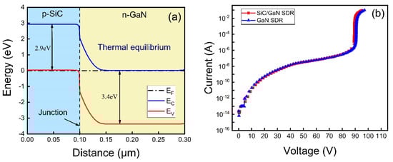
Figure 2.
(a) Thermal equilibrium state energy band diagram of SiC/GaN heterostructure (b) Breakdown characteristics of the two IMPATT diodes.
Figure 3 shows electric field distribution and impact generation rate of the two IM-PATT diodes under dc steady-state condition. The bias voltage Vdc is 97 V when the breakdown current reaches 0.1 A. On both sides of the avalanche junction in Figure 3a, the two IMPATT diodes have the same electric field distribution trend. As is shown in Figure 3b, the peak value of the impact generation rate on the right side of both p-n junctions is 1.31 × 1030/cm3/s. However, on the left side of the p-n junction, the two structures show obvious differences. The p-type SiC region of the heterostructure has obvious impact ionization, and its peak value can reach 1.40×1030/cm3/s, which is even higher than that of the n-type avalanche region. The electrons generated in this region are driven by the internal electric field into the GaN n-type avalanche region and subsequently into the drift region, which means we can predict that for the same design parameters. The SiC/GaN IMPATT has a higher avalanche injection charge, so it is expected to produce a higher rf output current. In contrast, GaN IMPATT does not demonstrate this phenomenon. From the above results, it can be seen that it is plausible to design IMPATT devices with a p-SiC/n-GaN heterojunction instead of GaN p-n junction in terms of the performance of dc characteristics. According to IMPATT efficiency prediction formula [30],
where φ is the phase delay between current and voltage. With the presence of impact ionization enhancement in SiC/GaN IMPATT diode, it is expected that the higher current Irf obtained in the new structure will result in better rf performance.
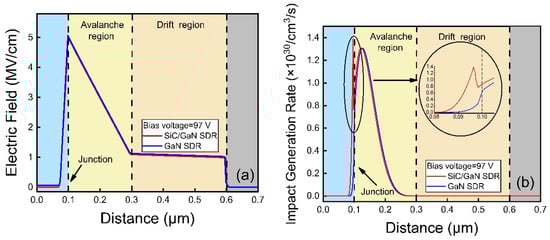
Figure 3.
(a) Electric field profiles, (b) Impact generation rates of the two diodes at 100 kA/cm2 reverse current density.
3.2. Large-Signal Simulation Results and Discussions
Firstly, we simulate the rf large-signal performance of the device by free-running circuit shown in Figure 1c. The inductance is adjusted by continuous trial and error, and a stable current-voltage waveform is obtained when the device’s own oscillation frequency matches that of the LC resonant circuit, at which point the resistance R is value of the negative resistance of the IMPATT diode in operation.
Figure 4 shows the maximum rf voltage, maximum rf current, and voltage-current phase delay of the diodes at different operating frequencies. As Figure 4a shows, under the same frequency, SiC/GaN IMPATT is able to output higher rf voltage, and consistently producing a voltage amplitude greater than 50 V in the frequency range from 160 GHz to 250 GHz. The rf voltage of SiC/GaN IMPATT reaches the maximum value of 51.6 V at 180 GHz, and then the voltage decreases with the increase of frequency. The GaN IMPATT has the same trend, but reaches the maximum value of 50.1 V at 160 GHz. The maximum rf current of SiC/GaN IMPATT increases as frequency increases, and when the frequency is higher than 250 GHz, it begins to decline. It is noted that the rf current generated by the SiC/GaN IMPATT is significantly higher than that of GaN IMPATT when the operation frequency is higher than 180 GHz. As shown in Figure 4c, the difference of voltage-current phase delay is also one of the reasons that effects the performance of IMPATT devices. At the same frequency, SiC/GaN IMPAT has a slightly larger phase delay. It can also be seen from Figure 4c that when the operating frequency is higher than 350 GHz, the phase delay of SiC/GaN IMPATT is reduced to below 90°, the negative resistance generation ability is lost, and the device cannot produce oscillation. However, in comparison, the phase delay of GaN IMPATT is reduced to 90° at 300 GHz, which means that SiC/GaN IMPATT has a higher operating frequency band and greater potential for high-frequency applications.
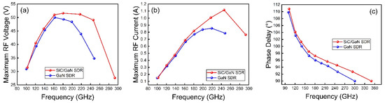
Figure 4.
(a) Maximum rf voltage, (b) Maximum rf current and (c) Phase delay of the two IMPATT diodes at different operation frequencies.
Figure 5 shows the curves of the negative resistance as a function of frequency for two diodes, which have the same value of the load resistance R in the free-running circuit. As the frequency increases, the negative resistance decreases. When the two devices work in the oscillation frequency range, the difference between the resistances is very small. Under the same operating frequency, the negative resistance produced by SiC/GaN IMPATT is slightly higher than that of GaN device.
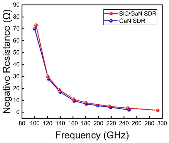
Figure 5.
Negative resistance characteristics of the two diodes.
Figure 6 shows the relationship between the negative conductance and frequency of the two diodes. It can be seen from the figure that the negative conductance increases with the increase of frequency at low frequencies, and then begins to decrease after reaching the maximum value. The highest conductance is obtained at 120–180 GHz for SiC/GaN IMPATT, which is 2.0 × 10⁻³ s/cm2, and 140–180 GHz for GaN IMPATT, which is 1.8 × 10⁻³ s/cm2. Obviously, the heterogeneous structure remarkably enhances the conductance characteristics of the device.
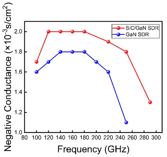
Figure 6.
The negative conductance of the two diodes is plotted against frequency.
Through the above parameters, we can obtain performance parameters such as the efficiency and rf power characteristics of the device. It can be seen that SiC/GaN IMPATT has a higher rf conversion efficiency and power density as shown in Figure 7. Meanwhile, it has a higher optimum frequency and larger frequency bandwidth.
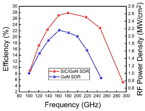
Figure 7.
The curves of efficiency and rf power at different frequencies for the two IMPATT diodes.
Table 3 shows the comparison of rf output performance of the two IMPATT diodes at their optimum frequencies. In the free-running circuit, the rf current, rf voltage, and phase delay between them determine the optimum power and efficiency obtained. The optimum dc-rf conversion efficiency and power density of SiC/GaN IMPATT are 27.8% and 2.67 MW/cm2, respectively, and the optimum frequency is 180 GHz. The optimum dc-rf conversion efficiency and power density of GaN IMPATT are 22.1% and 2.14 MW/cm2, respectively, and the optimum frequency is 160 GHz.
Table 3.
Comparison of rf output performance for the two IMPATT diodes.
Figure 8 shows the electron concentration distribution of SiC/GaN and GaN IMPATT in one oscillation period at their optimum frequency. The time interval is equal to 1/12 of the oscillation period. The working mechanism of IMPATT can be clearly seen in the Figure 8. Charge packets are continuously generated in the avalanche region, and their concentration rises until the charge packets mature. For SiC/GaN IMPATT, the charge packet concentration can reach a maximum of 1.83 × 1017 cm−3, higher than that of GaN IMPATT at 1.57 × 1017 cm−3, achieving more avalanche charge injection, which is attributed to the enhancement effect of avalanche for SiC/GaN IMPATT, as revealed in Figure 3b. According to IMPATT current formula [31]:
where Qava is the charge generated by avalanche multiplication and its movement WD is the length of the drift region, as a fixed value here. It can be calculated that a greater avalanche injection charge of SiC/GaN IMPATT makes a key contribution to its large external induced current. In the drift region, the charge packets are driven by the electric field and begin to transit. The phase delay between the rf voltage and current is due to the time for the generation and transit of charge packets, so negative resistance will be generated in the device, and then the dc power will be converted into rf output power. The visible increase of charge packet concentration and folding in the drift region, as shown in Figure 8, is attributed to the negative differential mobility (NDM) effect of GaN materials [25,32], which helps to significantly improve the rf performance of IMPATT devices. Therefore, combining with Figure 3b, it can be clearly seen that the avalanche enhancement phenomenon increases the injected charge packet concentration, which is one of the mechanisms for improving the performance of SiC/GaN IMPATT.
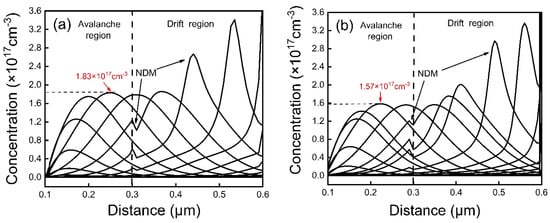
Figure 8.
Electron concentration distribution at 1/12 time interval in one oscillation period. (a) SiC/GaN and (b) GaN IMPATT at the optimum frequency.
Figure 9a,b show the electric field distribution of SiC/GaN and GaN IMPATT in an oscillation period at the optimum frequency, respectively. The time interval is a 1/7 oscillation period. VB is the dc breakdown voltage, when the rf voltage is higher than VB, the devices operate in the avalanche period, on the contrary, when rf voltage is lower than VB, the device operates in the drift period. In the avalanche region, the swing amplitude of the rf electric field of the two devices is roughly equivalent, and the maximum electric field has the same value, which is 5.9 × 10⁶ V/cm. However, in the drift region, the SiC/GaN IMPATT has a lower electric field distribution in drift period as curves 4,5,6,7 reveal. The lowest electric field of SiC/GaN IMPATT is 1.2 × 10⁵ V/cm as shown as curve 6 in Figure 9a. Figure 9b shows that the lowest electric field of GaN IMPATT is 2.32 × 10⁵ V/cm, and then gradually increases to 5.4 × 10⁵ V/cm as curve 6. Figure 10 is the electron velocity-field dependence of GaN material with and without negative differential mobility characteristics [25]. It can be seen that the electron velocity of the GaN material will even gradually increase to 2.9 × 107 cm/s when the electric field is lower than 6 × 10⁵ V/cm. Figure 9c,d show the electron velocity of SiC/GaN and GaN IMPATT in a drift period at the optimum frequency, respectively. The time interval is 1/6 drift time. It can be seen that SiC/GaN IMPATT has four curves in a drift period that can reach the peak speed as revealed by curves 2–5. This is because SiC/GaN IMPATT has a lower electric field value of 1.2 × 10⁵ V/cm, and combined with Figure 10, it can be seen that the electric field swing of the drift period is mostly distributed in the GaN negative differential mobility region in Figure 10 (between 1.2 × 10⁵ V/cm and 5.9 × 10⁵ V/cm), so there are several velocity curves that can reach electron drift velocities greater than the saturation value. In comparison, as shown in Figure 9d, GaN IMPATT has only two curves of electron velocity that can reach high values, as curves 3 and 4 reveal, and its lowest electric field is 2.32 × 10⁵ V/cm. Other drift period electric fields are all greater than this value. So, in combination with Figure 10, only one electron velocity curve can reach the peak value. In addition, the electric field at 0.55 μm in Figure 9b can rise to 5.4 × 10⁵ V/cm, and combined with Figure 10, the electron velocity of GaN IMPATT continues to decrease to a saturation constant value at 0.55 μm. Finally, the electron drift velocity in SiC/GaN IMPATT is significantly higher than that in GaN IMPATT in most parts of the drift region. Obviously, SiC/GaN IMPATT has a higher average electron velocity in the entire drift region owing to the lower electric field. Because GaN material has aa negative differential mobility effect, a lower electric field can make the electrons in GaN material reach higher drift velocity. According to IMPATT current Equation (7), νs is the average drift velocity that carriers can reach in a semiconductor device, which explains why SiC/GaN IMPATT has a higher rf output current and frequency bandwidth. In a word, the rf electric field in the drift region can obtain a larger swing to achieve a lower value, and this electric field modulation is another mechanism to improve the performance of SiC/GaN IMPATT.
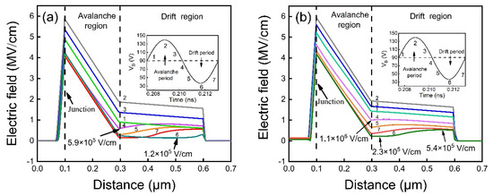
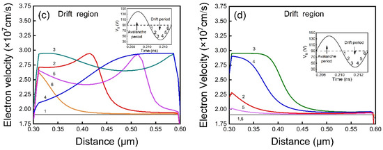
Figure 9.
Electric field distribution of (a) SiC/GaN, (b) GaN IMPATT in an oscillation period, electron velocity profiles of (c) SiC/GaN, (d) GaN IMPATT in a drift period at their optimum frequency, respectively.
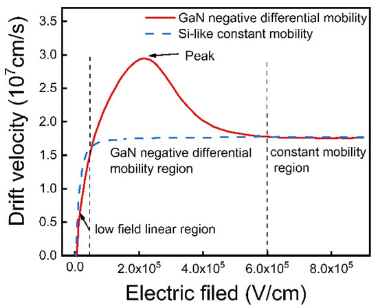
Figure 10.
Electron velocity-field dependence of GaN material with and without negative differential mobility characteristics.
Figure 11 shows the relationship between the optimum efficiency and the doping concentration of the p-SiC region or p-GaN region. We have found that the optimum frequencies of the two IMPATT diodes do not change with the increase of the doping concentration of the p-type region. If the doping concentration is increased, the optimum efficiency of SiC/GaN IMPATT is improved more significantly than GaN IMPATT, which means that we can improve the rf performance of SiC/GaN device by adjusting the doping concentration.
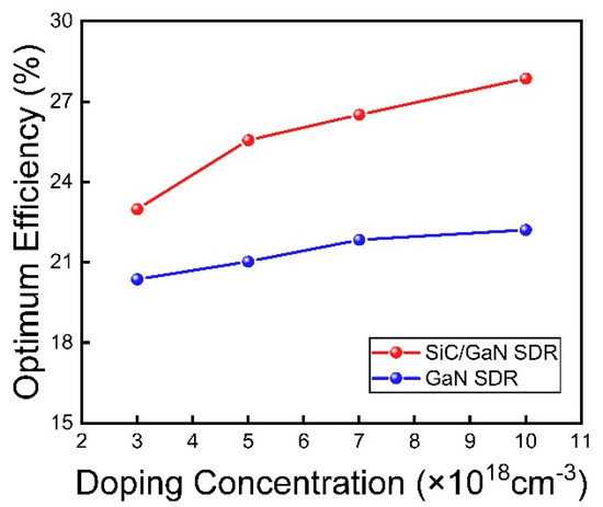
Figure 11.
The relationship between the optimum efficiency and the doping concentration of the p-SiC region or p-GaN region.
4. Conclusions
In this paper, a novel SDR IMPATT diode based on the heterojunction is investigated. The p-6H SiC/n-GaN heterojunction is proposed to replace the GaN homogenous p-n junction to manufacture an IMPATT diode and make it operate in IMPATT mode. The dc and rf performances of the new structure are studied in detail. Simulation results show that, on the one hand, the SiC/GaN hetero-structural IMPATT has the avalanche enhancement effect in the p-type SiC region, achieving excessive avalanche charge injection, and on the other hand, one can obtain a lower electric field distribution in the drift region, which results in a higher average electron velocity and current. These two mechanisms make the performance of the SiC/GaN IMPATT diode better than that of the GaN IMPATT diode. The optimum frequency, rf power, and efficiency of SiC/GaN IMPATT can reach 180 GHz, 2.67 MW/cm2, and 27.86%, respectively, while that of GaN IMPATT can reach 160 GHz, 2.14 MW/cm2, and 22.04%, respectively. The results also show that the performance of SiC/GaN IMPATT is improved with the increase of p-SiC doping concentration. In conclusion, the SiC/GaN IMPATT diode can be used as an alternative to the conventional GaN IMPATT diode. Additionally, it also provides a reference for a deeper understanding of the working mechanism and design of wide-bandgap semiconductor materials.
Author Contributions
Conceptualization, Y.D. and J.D.; data curation, J.D.; methodology, Q.Y. and Z.L.; software, S.Z.; validation, S.P.; formal analysis, X.L.; investigation, C.L.; writing—original draft preparation, Y.D. and J.D.; writing—review and editing, J.D., Y.Z. and H.Z.; funding acquisition, Y.D., X.L., Y.Z. and H.Z.; visualization, H.Z.; supervision, W.Z. All authors have read and agreed to the published version of the manuscript.
Funding
This work was supported in part by the National Natural Science Foundation of China under Grant 61804125, Grant 61701402, Grant 12004307 and Grant 62004163.
Data Availability Statement
Data presented in this study are available on request from the cor-responding author. The data are not publicly available due to internal policies of the industry research partner.
Conflicts of Interest
The authors declare no conflict of interest.
References
- Banerjee, M.S. THz solid-state source based on IMPATT devices. Terahertz Biomed. Healthc. Technol. 2020, 116, 1–41. [Google Scholar]
- Mukherjee, M.; Mazumder, N.; Roy, S.K.; Goswami, K. GaN IMPATT diode: A photo-sensitive high power terahertz source. Semicond. Sci. Technol. 2007, 22, 1258–1267. [Google Scholar] [CrossRef]
- Chen, K.J.; Häberlen, O.; Lidow, A.; Tsai, C.L.; Ueda, T.; Uemoto, Y.; Wu, Y. GaN-on-Si power technology: Devices and applications. IEEE Trans. Electron Devices 2017, 64, 779–795. [Google Scholar] [CrossRef]
- Millan, J.; Godignon, P.; Perpiñà, X.; Rebollo, J. A survey of wide bandgap power semiconductor devices. IEEE Trans. Power Electron. 2014, 29, 2155–2163. [Google Scholar] [CrossRef]
- Huish, P.W. A comparison between 20:1 and 5:1 doping ratios for high efficiency X-band GaAs IMPATT diodes. In Proceedings of the 7th European Microwave Conference, Copenhagen, Denmark, 5–8 September 1977; pp. 487–491. [Google Scholar]
- Read, W.T. A proposed high-frequency, negative-resistance diode. J. Bell Syst. Tech. 2013, 37, 401–446. [Google Scholar] [CrossRef]
- Ke, W.C.; Lee, S.J.; Chen, S.L.; Kao, C.Y.; Houng, W.C. Effects of growth conditions on the acceptor activation of Mg-doped p-GaN. Mater. Chem. Phys. 2012, 133, 1029–1033. [Google Scholar] [CrossRef]
- Dai, Y.; Yang, L.A.; Xu, S.R.; Hao, Y. Anisotropy effects on the performance of wurtzite GaN impact-ionization-avalanche-transit-time diodes. Appl. Phys. Exp. 2016, 9, 111004. [Google Scholar] [CrossRef]
- Li, X.; Yang, L.; Zhang, X. GaN/AlxGa1−xN/GaN heterostructure IMPATT diode for D-band applications. Appl. Phys. A 2019, 125, 205. [Google Scholar] [CrossRef]
- Fu, K.; Fu, H.Q.; Huang, X.Q.; Yang, T.H. Reverse leakage analysis for as-grown and regrown vertical GaN-on-GaN schottky barrier diodes. IEEE J. Electron Devices Soc. 2020, 8, 74–83. [Google Scholar] [CrossRef]
- Liu, J.; Yang, M.C.; Liu, C.; Liu, W.H.; Han, C.Y.; Zhang, Y.; Geng, L.; Hao, Y. Three orders of reverse leakage reduction by using supercritical CO2 nitriding process on GaN quasi-vertical schottky barrier diode. IEEE Trans. Electron Devices 2021, 68, 197–201. [Google Scholar] [CrossRef]
- Dai, Y.; Lu, Z.; Ye, Q. Study of InGaN/GaN Homotype Heterojunction IMPATT Diodes. IEEE Trans. Electron Devices 2021, 99, 1–7. [Google Scholar]
- Hba, B.; Bc, C.; Emf, D. Modeling the simultaneous effects of thermal and polarization in InGaN/GaN based high electron mobility transistors. Optik 2019, 207, 1–16. [Google Scholar]
- Chen, J.T.; Bergsten, J.; Lu, J. A GaN–SiC hybrid material for high-frequency and power electronics. Appl. Phys. Lett. 2018, 113, 041605. [Google Scholar] [CrossRef]
- Majewski, J.A.; Städele, M.; Vogl, P. Stability and Band Offsets of SiC/GaN, SiC/AlN, and AlN/GaN Heterostructures. MRS Proc. 1996, 449, 917–922. [Google Scholar] [CrossRef]
- Dai, Y.; Ye, Q.; Dang, J. Study of p-SiC/n-GaN Hetero-Structural Double-Drift Region IMPATT Diode. Micromachines 2021, 12, 919. [Google Scholar] [CrossRef]
- Bertazzi, F.; Moresco, M.; Bellotti, E. Theory of high field carrier transport and impact ionization in wurtzite GaN. Part I: A full band Monte Carlo model. J. Appl. Phys. 2009, 106, 63718. [Google Scholar] [CrossRef]
- Kamakura, Y.; Fujita, R.; Konaga, K. Full band Monte Carlo simulation of impact ionization in wide bandgap semiconductors based on ab initio calculation. In Proceedings of the 2016 International Conference on Simulation of Semiconductor Processes and Devices (SISPAD), Nuremberg, Germany, 6–8 September 2016; IEEE: Nuremberg, Germany, 2016; pp. 47–52. [Google Scholar]
- Kuznetsov, N.I.; Gubenco, A.E.; Nikolaev, A.E. Electrical characteristics of GaN/6H-SiC n-p heterojunctions. Mater. Sci. Eng. B 1997, 46, 74–78. [Google Scholar] [CrossRef]
- Moscatelli, F.; Scorzoni, A.; Poggi, A.; Cardinali, G.C.; Nipoti, R. Al/Ti Ohmic Contacts to p-Type Ion-Implanted 6H-SiC: Monoand Two-Dimensional Analysis of TLM Data. Trans. Tech. Publ. 2003, 433–436, 673–676. [Google Scholar] [CrossRef]
- Rizzi, A.; Lantier, R.; Lüth, H. Boundary Conditions and the Macroscopic Field at SiC/AlN and SiC/GaN Heterostructures. Phys. Status Solidi A-Appl. Mat. 2000, 177, 165–171. [Google Scholar] [CrossRef]
- Reklaitis, A.; Reggiani, L. Monte Carlo study of hot-carrier transport in bulk wurtzite GaN and modeling of a near-terahertz impact avalanche transit time diode. J. Appl. Phys. 2004, 95, 7925–7935. [Google Scholar] [CrossRef]
- Farahmand, M.; Garetto, C.; Bellotti, E.; Brennan, K.F.; Goano, M.; Ghillino, E.; Ghione, G.; Albrecht, J.D.; Ruden, P.P. Monte Carlo simulation of electron transport in the III-nitride wurtzite phase materials system: Binaries and ternaries. IEEE Trans. Electron Devices 2001, 48, 535–542. [Google Scholar] [CrossRef] [Green Version]
- Yang, L.A.; Hao, Y.; Yao, Q.Y.; Zhang, J.C. Improved negative differential mobility model of GaN and AlGaN for a terahertz Gunn diode. IEEE Trans. Electron Devices 2011, 58, 1076–1083. [Google Scholar] [CrossRef]
- Dai, Y.; Yang, L.A.; Chen, Q.; Wang, Y.; Hao, Y. Enhancement of the performance of GaN IMPATT diodes by negative differential mobility. AIP Adv. 2016, 6, 055301. [Google Scholar] [CrossRef] [Green Version]
- Luy, J.; Kuehnf, R. Tunneling-assisted IMPATT operation. IEEE Trans. Electron Devices 2002, 36, 589–595. [Google Scholar] [CrossRef]
- Elta, M.E.; Haddad, G.I. High-Frequency Limitations of IMPATT, MITATT, and TUNNETT Mode Devices. IEEE Trans. Microw. Theory Tech. 1979, 27, 442–449. [Google Scholar] [CrossRef]
- Kane, E.O. Theory of Tunneling. J. Appl. Phys. 1961, 32, 83–91. [Google Scholar] [CrossRef]
- Elta, M.E.; Haddad, G.I. Mixed tunneling and avalanche mechanisms in p-n junctions and their effects on microwave transit-time devices. IEEE Trans. Electron Devices 1978, 25, 694–702. [Google Scholar] [CrossRef]
- Misawa, T. Saturation current and large-signal operation of a read diode. Solid-State Electron. 1970, 13, 1363–1368. [Google Scholar] [CrossRef]
- Sze, S.M. Physics of Semiconductor Devices, 3rd ed.; Wiley: Hoboken, NJ, USA, 2006; pp. 466–509. [Google Scholar]
- Culshaw, B.; Giblin, R.A.; Blakey, P.A. Avalanche diode oscillators. I. Basic concepts. Int. J. Electron. 1974, 37, 577–632. [Google Scholar] [CrossRef]
Publisher’s Note: MDPI stays neutral with regard to jurisdictional claims in published maps and institutional affiliations. |
© 2021 by the authors. Licensee MDPI, Basel, Switzerland. This article is an open access article distributed under the terms and conditions of the Creative Commons Attribution (CC BY) license (https://creativecommons.org/licenses/by/4.0/).