1. Introduction
The multi-standard RF front-end is a continuing research challenge in the B5G/6G legacy, and has focused on high integration level and energy-aware hardware components to support a plethora of smart devices [
1]. The Power Amplifier (PA) is a key component of the energy-efficient RF front-end, being the highest power consumer of the RF transceiver architecture. In this context, the linearity efficiency and bandwidth performance are critical, and accordingly constitute a figure of merit of any amplifier design.
To overcome the bandwidth efficiency challenges associated with high-peak-to-average power ratio systems, numerous techniques representing significant progress toward realizing wideband and highly efficient RF and microwave PAs have been reported for various semiconductor technologies. The dynamic load modulation Doherty PA (DPA), introduced in 1936 [
2], combines the output power (
) of two active devices that operate as the main and peaking PAs through a load modulation network. It can maintain moderate- to high-efficiency operation across a large power range. Compared to the Outphasing, Envelope Tracking (ET) and Envelope Elimination and Restoration (EER) architectures [
3], DPA features simple circuit implementation that allows wideband operation. Therefore, it is one of the most widely used techniques for cellular Base-Stations (BSs) to amplify the modulated signals with high crest factors; indeed, it has been extensively explored for use in upcoming B5G multicarrier applications.
Recent advancements in DPA topologies elucidate its applicability at mm-wave frequencies [
4]. However, the main disadvantages of DPA implementation lie in its nonlinear distortion and intrinsic bandwidth limitations. The average efficiency solutions, including bias adaptation mechanisms, phase synchronization, stacked-type devices, low-loss combiner, waveform-engineering, balance compensation Marchand balun and transformer-based DPAs, have been adapted individually or in synergy, while the harmonics can be well-controlled [
5,
6,
7,
8,
9]. Accordingly, the configurations of concurrent reconfigurable or dual-band distributed DPAs can expand the frequency response and bandwidth (BW) operation [
10,
11,
12,
13]. Some of the previously reported approaches of the reduced transformation ratio, the quasi-lumped impedance inverter, and the planner network and transformerless topologies, by absorbing the effects of the parasitics, enable modified power combining [
14]. Recently, it has been shown that inserting a compensation reactance at the combining point of the main and peaking PAs can effectively expand the BW [
15]. Nevertheless, most of the broadband DPA approaches have been developed for sub-6 GHz band frequencies based on discrete technologies, while at mm-wave frequencies, the extensive power losses, large parasitic components, current density limitation, and transmission line mutual coupling coefficient present obstacles to the deployment of functional fully integrated IC DPA systems. These challenges reduce the effectiveness of the bandwidth extension techniques reported in the literature, and indicate the need for further research efforts.
The watt-level K-band DPA presented in [
16] allows for broadband dual-driver operation that absorbs the parasitics encountered in the nonlinear model. The fabricated DPA exhibits a 2.4 GHz bandwidth as well as 38% PAE at the peak
of 30 dBm, where the occupied chip size is around 4.3 mm
2. An E-mode GaAs DPA for the mobile terminals, with a compact chip size of 2.86 mm
2, is reported in [
17], which employs a meander broadside coupler. The reported DPA delivers a maximum PAE value of 40% at the peak
for 26 dBm, and 29% at 6 dB PBO for 28 GHz. A high power density of 28.7 dBm at Ka-band frequencies is achieved in [
18] by taking advantage of the gate capacitance in stacked transistors. The proposed DPA at 28 GHz delivers a 27% PAE at 6 dB PBO within the chip size of 5.1 mm
2. In [
19], a 25 dBm dual-band DPA operating at 29 and 46 GHz exhibits 22% PAE at 6 dB PBO, where a reversed uneven power splitter is adapted to enhance the gain performance; however, the large insertion loss of dual-band transmission lines does not comply with the strict design rules of IC technology, and results in low average efficiency.
Low-power mobile handset PA module design requires challenging tradeoffs among small size, wide band, high efficiency, high gain, and linearity. Therefore, a limited number of handset DPAs in the mm-wave region have been reported to date, providing up to 28% PAE at the PBO. This paper intends to develop an ultra-compact load modulation technical approach for wideband scenarios, targeting next-generation B5G/6G mobile handsets. To achieve this goal, turning to the miniaturized size of the MMIC technology, an asymmetrical DPA architecture design is proposed based on the modified Class-J mode of operation, including accurate guidelines to select an optimum impedance at PBO. The proposed DPA at K-band frequencies employs a low-pass post-matching network, along with multi-section impedance matching networks at the output for broadband operation.
The outline of the paper is as follows:
Section 2 describes the features of the mobile handset semiconductor technologies and their suitability applications; the design approach for a high-gain and wide-band two-stage DPA is presented in
Section 3; the large-signal simulation results of the pHEMT device, as well as the performance comparison of the proposed DPA with recently reported mm-wave DPAs, are discussed in
Section 4; finally, some conclusive remarks are given in
Section 5.
2. Technology Selection
The MMIC technology enables an ultra-compact PA circuit configuration, and offers the potential advantages of thin metal thickness, a multistage design for higher gain, better amplitude and phase tracking, higher operating frequency, broadband performance, circuit design flexibility, and greater reliability. GaAs is widely accepted as a superior technology, with excellent features for small-dimension and high-frequency coverage for handset applications [
20]. The semi-insulating substrate property of the GaAs enables high carrier mobility and fast switching at low intensity, which contribute to its long-term operation. InGaP HBT benefits from high current gain and single power supply polarity, and can downsize the module area within the cell phone front-end PAs. However, the GaAs heterojunction bipolar transistor (HBT) device’s nonlinearities influence the ideal gain characteristics and reduce its optimum operation. In general, the imbalance in the thermal region due to the mismatch of the entire HBT geometry for small-scale emitters causes heat dissipation [
21]. On the other hand, GaAs pseudomorphic high-electron mobility transistor (pHEMT) technology facilitates the monolithic integration of low-noise and low-loss passive components covering sub-6 GHz to mm-wave band frequencies. In fact, it is more reliable at low-voltage operation in terms of thermal runaway, possessing the advantages of high gain, good linearity and great transition frequency. In this work, the WIN semiconductors process design kit (PDK) with the AlGaAs–InGaAs pHEMT technology and a 0.1
gate length is utilized. The PP-10 process is qualified for 4 V operation on a substrate thickness of 50
, including two metal layers. The maximum frequency (
) and the cutoff frequency (
) are 180 GHz and 132 GHz, respectively. Moreover, this process offers metal–insulator–metal (MIM) capacitors with 406
density.
3. Wideband and Compact Circuit Design Procedure
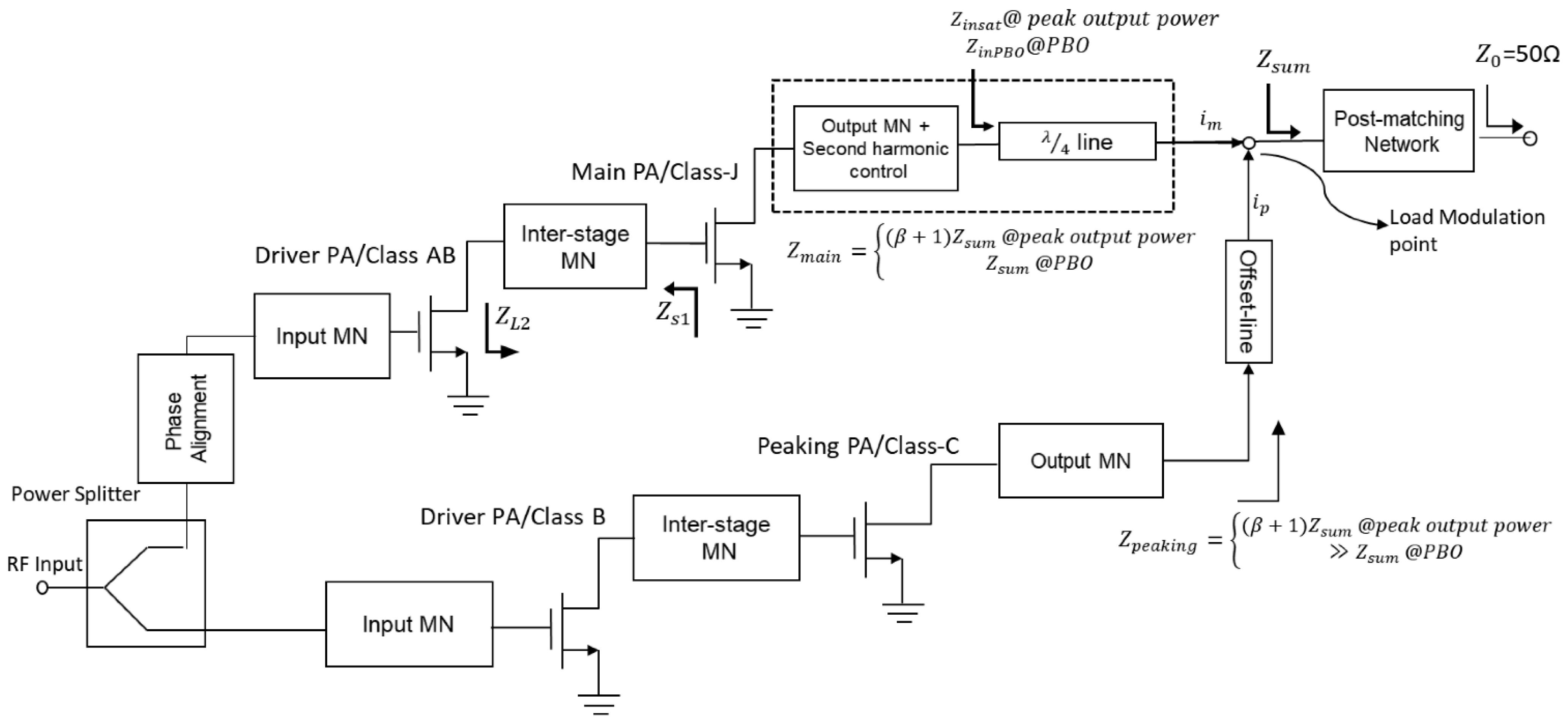
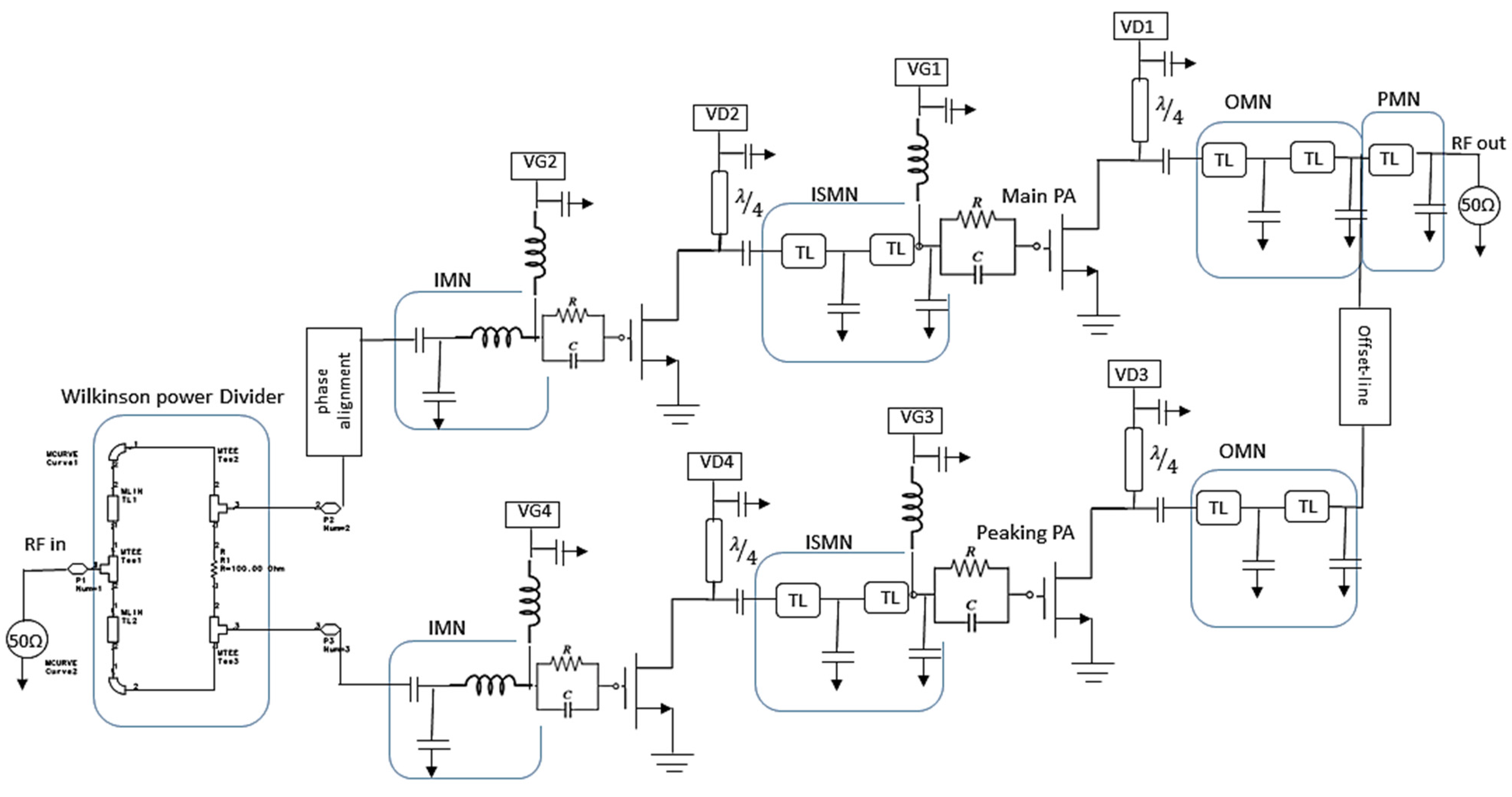
Figure 1 presents the general architecture of the proposed two-stage MMIC DPA. It includes a power stage, providing the target
of 1 W, and a driver stage to enhance the overall power gain. Subsequently, it consists of input-matching networks (IMNs), inter-stage-matching networks (ISMNs), and output-matching networks (OMNs), which provide for harmonic tuning as well as the biasing feed. The main PA benefits from the second harmonic voltage enhancement using the modified Class-J mode of operation [
22]. The DPA features an asymmetrical size ratio in the active devices to guarantee maximum
and the reduced characteristic impedance of the impedance inverter in the load modulation network. The characteristic impedance of the inverter line is derived from the optimum impedance of the main and peaking PAs at the peak power and targeted back-off levels. Since the bandwidth of the DPA relies on the load modulation equivalent circuit, the optimized transformation ratio results in the wide frequency response of the main PA, and the consequent bandwidth extension of the DPA. A phase-compensation network in the input path of the main PA is tuned to align the phase and to ensure the constructive combination of the two signals arising from the output of the main and peaking paths. Finally, a Wilkinson splitter provides in-phase input power for both PAs, while its two output terminals are isolated from one another.
The load modulation Doherty technique operates the principle of the load pulling through the output current of the peaking device. In the symmetrical DPA, the power ratio () of the main and peaking PAs ( is equal to one, which delivers 6 dB PBO efficiency, since the PBO = 20.
Considering the peak-to-average power ratio (PAPR) of a modulated signal is typically 8.5 dB, an asymmetrical DPA
with larger PBO efficiency is a common design requirement. The output currents of the main and peaking PAs
and
have the same ratio as the power (
in the saturation region, as long as the voltage is constant. The impedance at the summation point of two active devices (load modulation point) can be given by:
where
and
are the optimum impedances of the main and peaking PAs at the peak power. The proposed design technique is based on the load-pull data of the optimum impedances at peak power and PBO; therefore, the characteristic impedance of the impedance transformer is defined according to the impedance at the summation point. When both amplifiers contribute equally at higher power levels,
and
can be obtained from (2) and (3):
where the impedance encountered at the input of the impedance inverter
line (
) is given by (4). Therefore, the maximum
of the main PA and the total output power (
) can be expressed as
At the PBO, when the peaking PA is turned off,
and
. Consequently, the impedance of the main PA (
) is equal to the summation point impedance of
. Hence, the impedance encountered at the input of the
line (
) will be increased, as follows:
Thus, the ratio of the optimum impedance of the main PA at the PBO (
) and at the peak power (
), where
and
, can be achieved by
Accordingly, the power ratio at PBO and saturation is given by (12),
The post-matching network at the output of the DPA transfers the common load impedance of 50 Ω to a lower impedance (), which is close to the optimum impedance of the main and peaking PAs at peak power. In this work, is selected as the real impedance of 30 Ω. With the equal contribution of two current sources, the impedance of the main and peaking PAs is 2 = (). At PBO, the peaking PA must be close to infinity, with an offset line embedded in its OMN; therefore, the impedance of the main PA is equivalent to . Hence, the load modulation increases the load encountered by the main PA by a scaling factor of , resulting in higher efficiency at the PBO.
3.1. Stability of the Transistor Cell
The output power is proportional to the device size, since it is a function of drain voltage, drain current and efficiency. By enlarging the transistor size dimension, the will be enhanced up to a certain size, determined by the breakdown voltage. However, there is a trade-off between maximum and high gain. Due to the thermal issues and parasitic effects associated with a larger device, as the device size increases, the available gain and efficiency will be degraded. As a consequence, by expanding the gate periphery (unit gate width × number of gate fingers), the maximum can be achieved by considering the power density and gain drop at saturation. Furthermore, to achieve the target gain specification, additional driver stages can guarantee optimum gain flatness. It should be noted that driver stages can improve the overall device gain at the cost of DC power consumption and bandwidth shrinkage; therefore, it is more desirable to employ fewer stages with higher gain.
In the current design, based on the bias condition and the 1 dB compression point, the power density of the selected design kit process has a gate width of 890 mW/mm. To achieve a 30 dBm output from the DPA, an 800 μm transistor is required for the main PA in order to provide the of 27 dBm. Thus, a total of eight fingers are chosen and arranged in an 8 × 100 μm transistor width configuration in the main path. Since the design is optimized for an asymmetrical DPA, in order to generate a high current and the maximum power in the peaking device in the saturation region, the size of the peaking device is set to 12 × 100 μm transistor width. Adapting a two-stage corporative topology for higher gain, the driver stage enables us to drive the final stage into compression. Assuming a 2 dB loss in the inter-stage matching network, the required power level at the output of the driver stage should only be 3 dB lower than that of the final stage. Taking into account the width ratio of 0.5:1 between stages, a driver cell of 4 × 100 μm transistor width can reduce the power consumption.
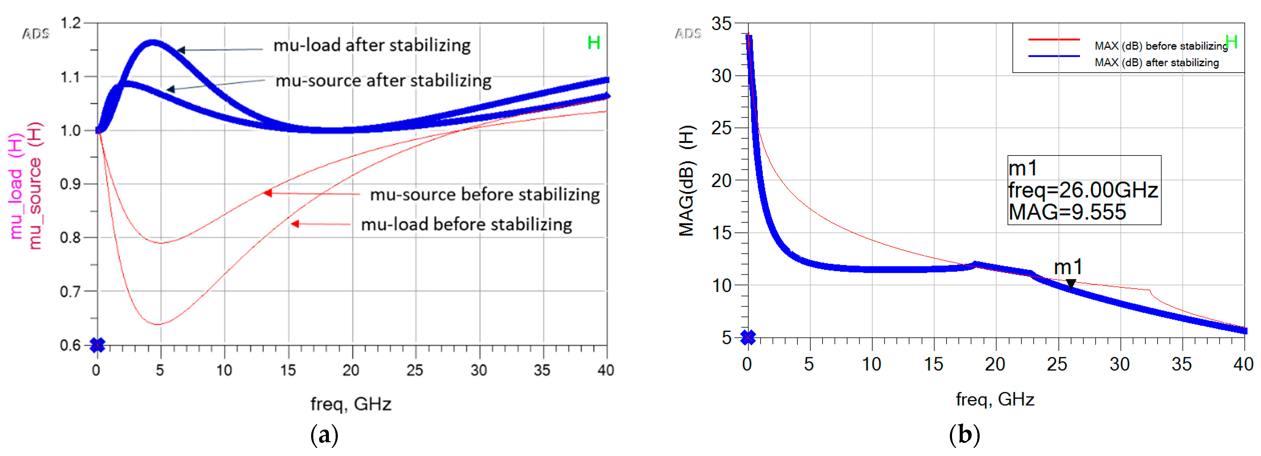
Prior to determining the power gain and saturated power of the transistor cells, it is essential to analyze the small-signal stability of the biased transistors so as to guarantee that no oscillation phenomena will arise, using Rollet’s linear
factors, as well as the geometrically derived (
) factor. In the first step of DPA design, to make the transistor unconditionally stable, a parallel RC network is located in series with the gate path, which increases the input impedance of the transistor at lower frequencies and provides good flexibility to shape the gain. The parallel capacitance decreases the equivalent impedance of the stability network at higher frequencies. The source and load
factors, before and after stabilizers, are depicted in
Figure 2a for the main transistor. As can be seen, the
source and load criteria are greater than one at all frequencies after stabilizing and any impedance of the Smith Chart is suitable for matching.
Figure 2b plots the effect of the stability network on the maximum available gain (MAG). The RC network introduces a dissipative loss, which decreases with frequency. A comparison between MAG without stabilization networks and MAG with an RC network reveals the small-signal gain reduction that occurs at the expense of decreasing the probability of parametric and out-of-band oscillations. The MAG at the main transistor is degraded to around 1.5 dB at 26 GHz under the same bias condition.
3.2. Output Matching Network Design
Most of the reported DPAs are developed under the framework of the Class AB/B and C modes of operation, with the aim of eliminating high-order intermodulation distortion. However, in the Class-C biased peaking PA, the gain expands as the input power increases, whereas for the Class-AB-biased main PA, the gain compresses with load modulation when the input impedance is nearly constant [
23]. The gain compression of the main PA can be suppressed by maintaining a proper bias condition in the device. Further, precise harmonic load termination can help to alleviate the intermodulation distortion (IMD) between devices [
24]. In this study, to achieve linear DPA performance, the main PA is biased for Class-J/B operation at the threshold of −0.8
, while the peaking PA is biased for a Class-C conduction angle at −1.6
.
It is proved that employing Class-AB mode in the Doherty structure, with a resistive load at the fundamental and short-circuiting all harmonics, can optimize the overall linearity. Besides, S. C. Cripps [
25] proposed the Class-J mode of operation, which offers the same efficiency and linearity as Class-AB or Class-B PAs across a broad frequency range. Class-J PA increases the fundamental voltage component, assisted by the second-harmonic voltage as a capacitive load. The initial principle of the Class-J PA is to shift the phasing of the drain current and voltage waveforms. The overlap between the waveforms introduces a pure reactive component that can be utilized to terminate the second harmonic and broaden the bandwidth. The drain voltage and current waveforms are characterized by half-sinusoidal waves, and can be expressed by the Fourier series expansion:
where
is the phase shift between the waveforms that increases the fundamental voltage component but reduces the optimal efficiency. On the other hand, second harmonic load termination plays an important role in accurately cancelling out the nonlinear output capacitance (
). The Class-J concept is further extended as the reactive second harmonic introduced by the output capacitor is injected into the drain node of the main PA [
26]. When the device is terminated by the optimum fundamental impedance, the nonlinear performance of the output capacitator as an out-of-phase second harmonic voltage can enhance the maximum possible drain voltage, which translates into higher efficiency.
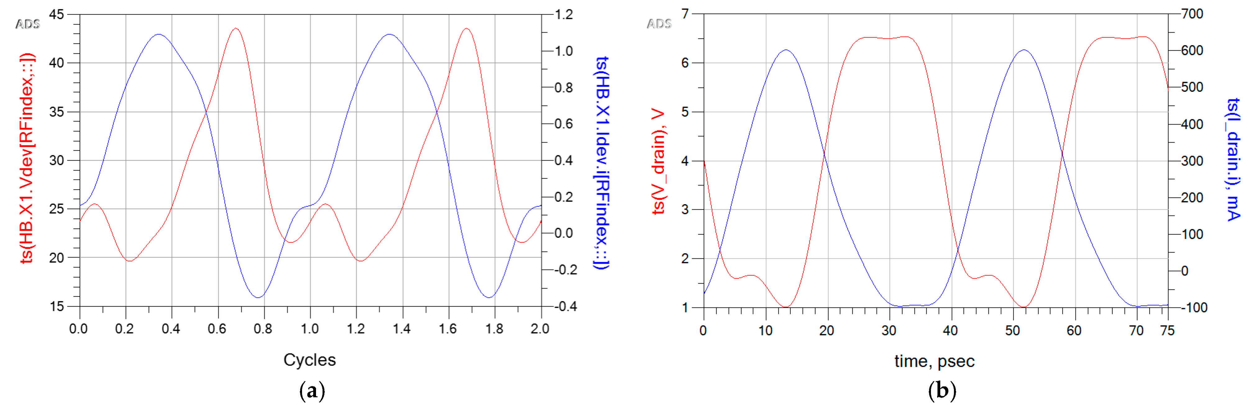
Figure 3 compares the simulated drain waveforms of the conventional Class-J PA operation, which constitutes the second harmonic voltage component, with those of the modified one.
In
Figure 3a, the 45
overlap between the half-sinusoidal current and the voltage waveforms degrades the optimum output power and drain efficiency. Moreover, the drain current deviates from the ideal half-sinusoidal shape due to the suboptimal second-harmonic impedance termination and the parasitics of the transistors. Conversely, the approximated square-wave drain-source voltage of the modified Class-J PA, shown in
Figure 3b, is increased by the impedance of the nonlinear output capacitor, which is smaller than the external second harmonic loading. Therefore, the phase mismatch between the voltage and current waveforms is reduced, yielding smaller power dissipation. The
parameter can be extracted using the optimum load admittance observed in the extrinsic transistor. The imaginary part of the load admittance must be canceled out by the output capacitance’s susceptance.
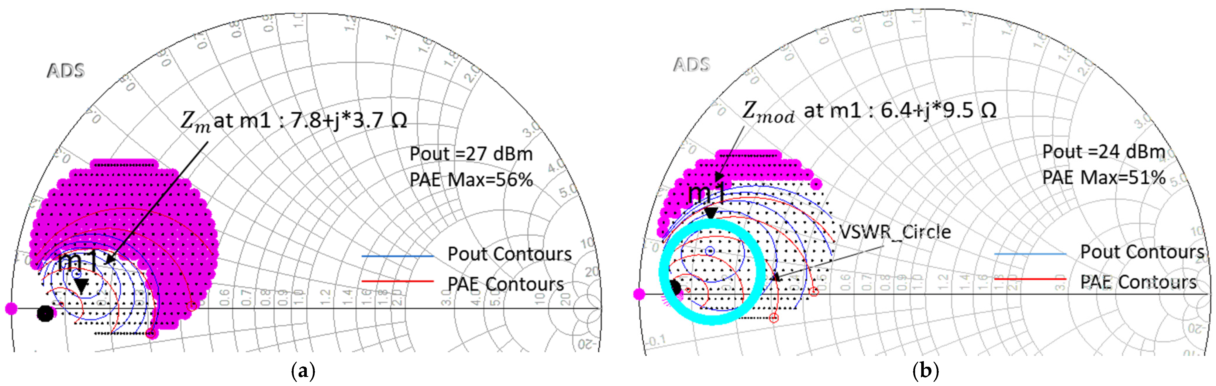
In the current design, the optimum load impedance that maintains a balance between maximum output power and maximum efficiency when the device is driven well into compression is determined by the load-pull simulations performed at several frequencies, from 24 GHz to 28 GHZ. As shown in
Figure 4a, the optimum impedance is located at
7.8 + j* 3.7 Ω at a 27 dBm output power. It should be noted that the stability circuit is also included in the load-pull simulation. The output capacitor can be calculated by (
) when
cancels out the susceptance of
.
The main PA is always on, and handles the signal at average power. To provide a compact matching design, the line impedance transformer is absorbed into the output matching network (OMN) of the main PA. Hence, the OMN is designed to present the desired load inversion at the PBO and peak power.
Having obtained the
and efficiency contours in
Figure 4, the load-pull simulation is conducted for an average
of 24 dBm, which is 6 dB lower than the target
of 1 W for DPA. The optimum impedance of the main PA at PBO will be determined by drawing the voltage standing wave ratio
circle using Equation (9). Therefore, in order to maintain the power ratio between the main and peaking PAs, the circle of
in
Figure 4b, centered on the optimum impedance at peak power (
, is drawn to determine the
. In this way, the optimum impedance at the PBO can be selected on the overlap between the VSWR circle and the efficiency contours (
= 6.4 + j* 9.5 Ω).
The OMN of the main PA performs the fundamental load impedance inversion by matching 2 to for the peak power, considering that = 1 in Equation (3), and at the same time transferring to for the PBO. It should be noted that the OMN adopts the capacitive second harmonic load termination generated by the profile. Thus, the calculated output capacitor of 0 – j* 2 Ω is injected into the second harmonic load component. Once the design of the OMN of the main PA is completed, the peaking PA, which only handles signal peaks, requires an OMN to transfer the to the optimum impedance at 27 dBm ( 3.5 + j* 3.6) at saturation. In order to prevent power leakage during low-power operation, the peaking PA employs a tuned offset line to provide a phase shift between the devices.
The BW of the DPA can be extended by improving the frequency response of the OMNs. Therefore, the multi-section matching network consists of series inductances, with shunt capacitances to match the impedances. Since the losses of the OMN degrade the optimal , the spiral inductors are replaced by double-metal microstrip lines with minimum ohmic loss in parallel with MIM capacitors. In the current design, the OMN is optimized for best performance under large-signal conditions.
3.3. Interstage and Input Matching Networks Design
The best overall PA efficiency in the multi-stage PA design is provided by the PAE of the output stage. Since the output stage must be driven well into the saturation region for maximum and efficiency, the driver stage is designed to provide sufficient power to the next stage, hence the peak PAE increases up to the dB compression point. Here, the optimum that can drive the succeeding stage into saturation is calculated to be 19 dBm, according to the gain of the main PA (8 dB). In the case of the peaking PA, due to the very low power gain of the Class-C mode, a higher is required for the driver PA (21 dBm) in the peaking path. It should be noted that the driver stage is expected to operate linearly, and should not reach the 1 dB compression point before the final stage. The driver PA for the main path is biased in the Class-AB mode (0.6 ). The small-width transistor with lower gate loss can improve the power gain; however, the output impedance of the smaller device is normally located in a highly loaded Q factor circle within the Smith Chart, which can restrict the circuit bandwidth. In this respect, the broadband DPA operation can be restored by selecting the proper load impedance at the overlap between the gain and the efficiency contours, characterizing by several frequencies in the band of interest.
The ISMN is required to transfer the output power of the driver stage into the input of the final stage. As can be seen in
Figure 1, it matches the source impedance (
of the final stage into the optimum load impedance (
of the driver stage. The ISMN must perform these functions with minimum losses, since losses of ISMN reduce the power gain and narrow the bandwidth. The most challenging part is designing the ISMN when the impedance transformation ratio between the stages is very high. Here, the large device at the output stage implies small input impedance (
2.4 – j* 12.7 Ω); hence, the ISMN is optimized with a low-pass-matching network to transfer the conjugate of the input impedance to the load impedance of the driver PA (
10.8 + j* 9.3 Ω) for the main path. The same technique should be applied to the peaking path. It should be noted that the gate bias line of the final stage and the drain bias line of the driver stage are both embedded in the ISMN, with DC separation between the bias suppliers of the preceding and following stages.
The IMN provides the optimal matching between the input impedance of the driver stage (
3.5 − j* 22 Ω) and 50 Ω source impedance. Although the transformation ratio of the IMN is also high, the losses have a negligible effect on the overall efficiency. The complete schematic of the designed DPA is depicted in
Figure 5. To limit the die area, the IMN is synthesized using a lumped-element network comprising spiral inductors and MIM capacitors. The bias lines employ an RF choke, which is typically realized by either a large inductor, or a quarter-wavelength distributed microstrip line (
) with low parasitics connected to a large bypass MIM capacitor near the bias supply. The width of the drain bias line should be specified by the current density limitation of the PDK process. For DC blocking, large capacitors in series with matching networks are deployed to avoid a dielectric breakdown in the transients.
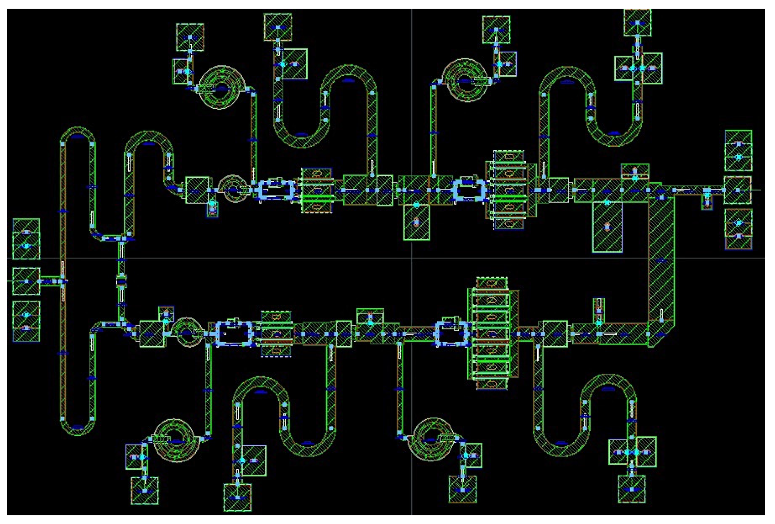
Figure 6 illustrates the final layout of the presented DPA with a die area of 2.3 × 1.4 mm
2, including OMN, ISMN and IMN stages. The real-to-real impedance transformation at the output of DPA maximizes the bandwidth and power transformation. The gain equalizer sub-networks are located in the devices gate path to compensate the gain roll-off. The effect of the electromagnetic coupling degrades the PA performance in the compacted MMIC layout at the K-band; therefore, EM simulation is critical to ensure the accuracy of the design rules. In this work, Momentum is used to characterize the spiral inductors and to capture any coupling between transmission lines. In the ADS circuit design environment, the EM models of the matching networks are separately generated for S-parameter models, which will be used in the co-simulation stage.
4. Simulation Results, Comparison and Discussion
To analyze the circuit performance, the nonlinear model provided by the foundry is utilized to run extensive Harmonic Balance (HB) simulations sweeping RF-power, frequency and DC current components to observe the large-signal performance of the designed DPA.
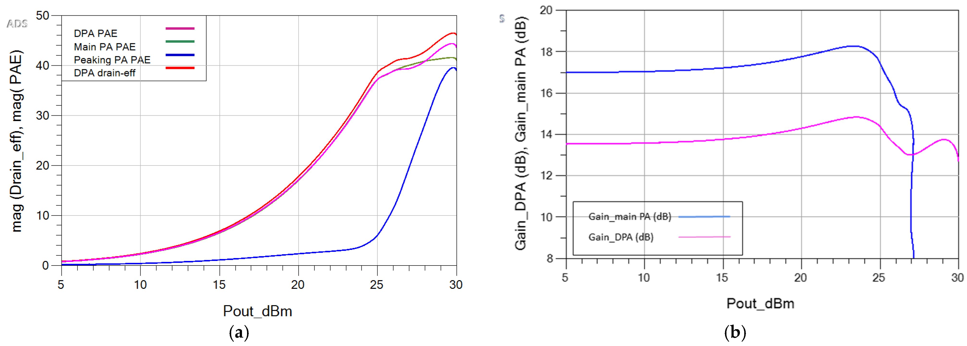
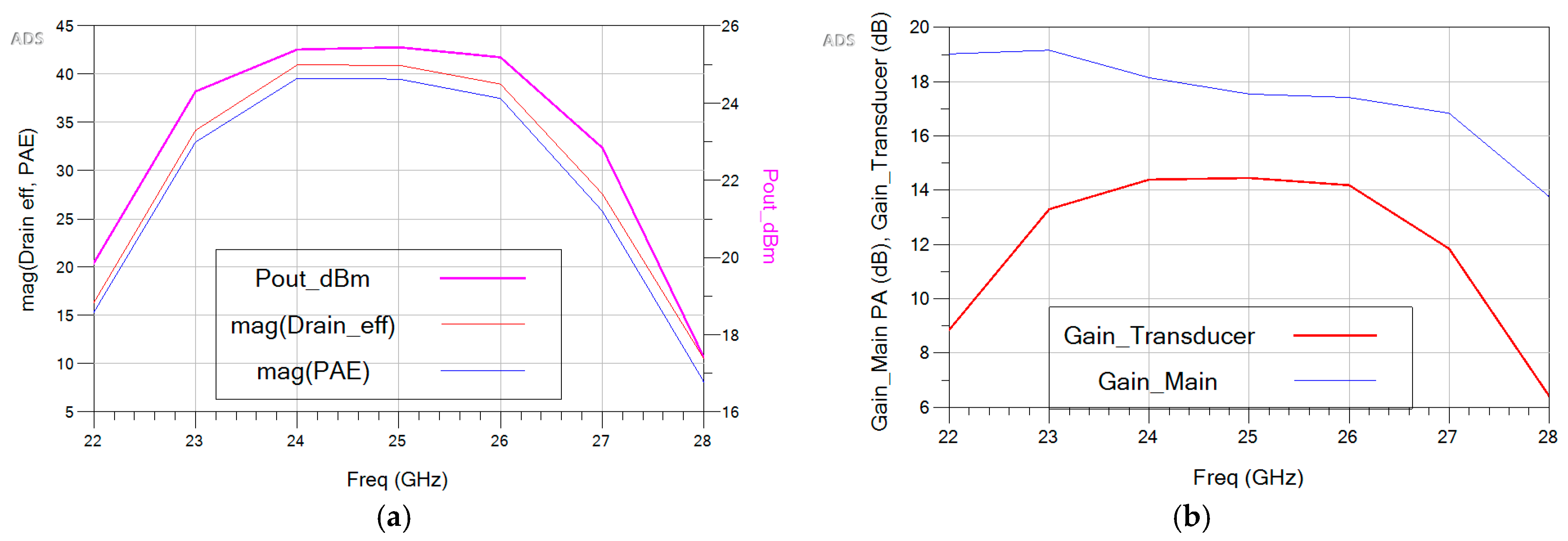
Figure 7a plots the simulation results of the PAE and the drain efficiency of the DPA as a function of the
. The maximum
at the 1dB compression point of the DPA is 30 dBm. It can be seen that the K-band MMIC DPA achieves 47% drain efficiency and 44% PAE at 1 W
, and 34% PAE at 6dB PBO.
Figure 7a also compares the PAE of the main PA and the peaking PA with the overall DPA PAE. The linearity and efficiency of the DPA depend on the turn-on timing of the peaking PA. The simulation result shows that the Class-C peaking PA contributes to current conduction when the main PA starts to compress, leading to high PAE. This can guarantee the flatness of DPA power gain. The evaluation of the linear operation is based on the power gain, IMD, and the phase difference between the input and output signals.
Figure 7b shows the gain flatness of the DPA, which is almost 3dB less than that of the main PA (17 dB) due to the 3 dB coupler at the input of DPA; this reduces the input power level of the main PA by 3 dB; therefore, the overall power gain of the DPA is 14
0.5 dB. The gain reduction of the main PA is compensated for by the peaking PA at high power levels by selecting a larger device size.
.
Once the main PA is saturated by the 3 dB compression, the peaking PA provides more power, thus assisting the DPA’s large signal gain operation. The DPA is likely to be linear as long as the gain characteristic in the modulation region remains constant.
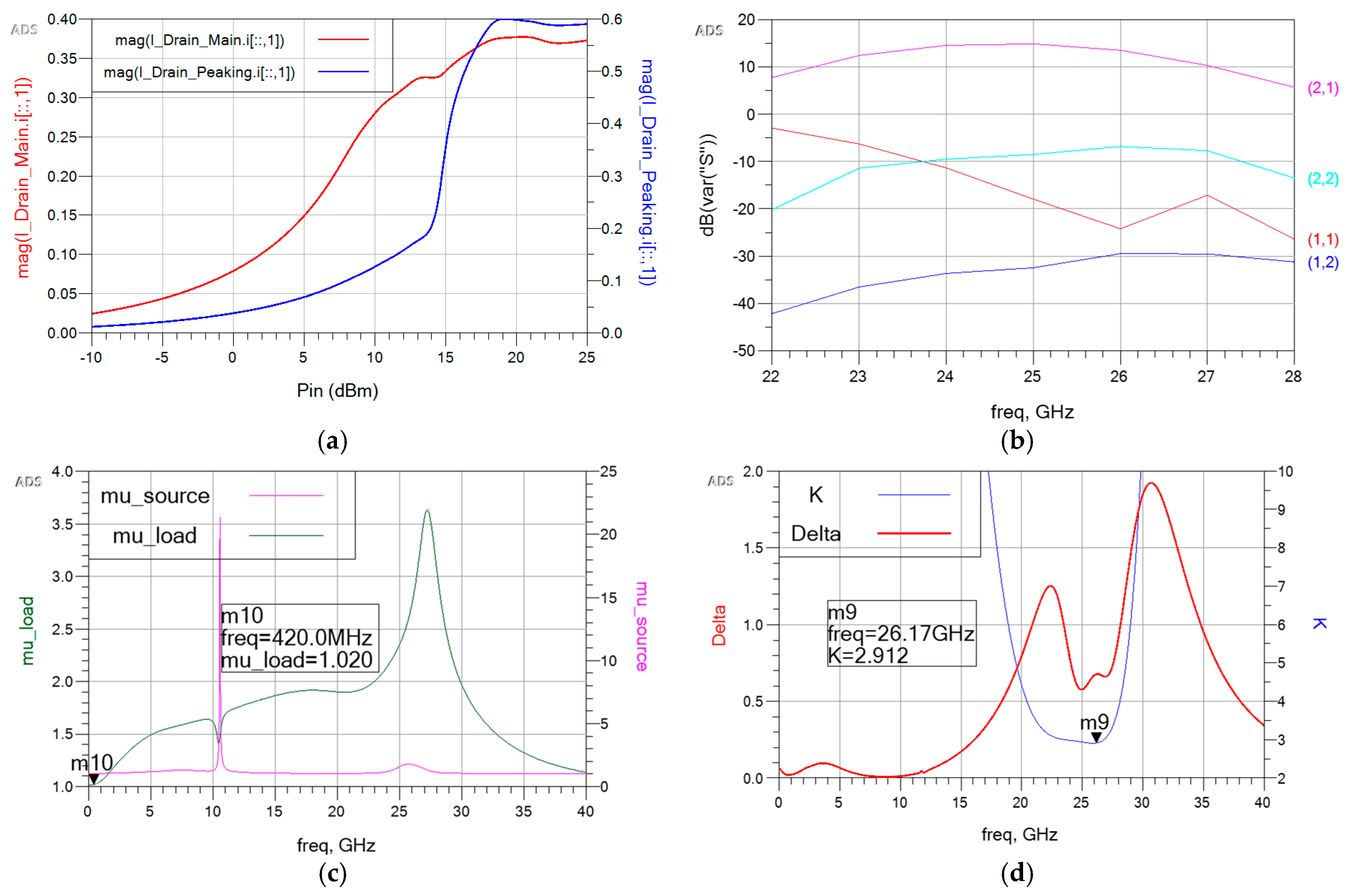
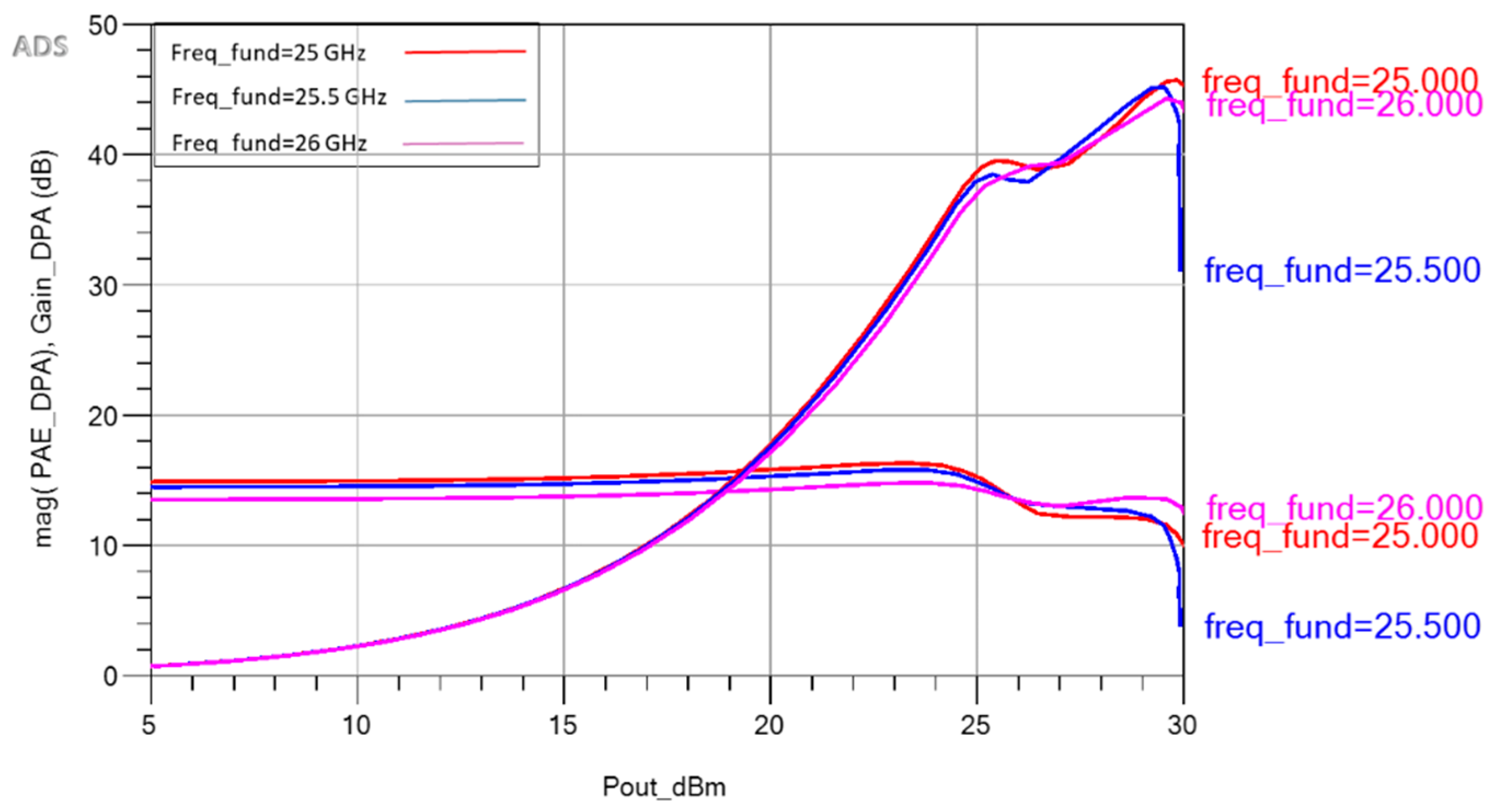
Figure 8 illustrates the similar efficiency and power gain performance of the DPA for frequencies 25, 25.5 and 26 GHz. In the target bandwidth, the variations in the power gain, PAE and drain efficiency at the input power of 10 dBm in
Figure 9a,b indicate that the PAE varies between 32% and 40%, reaching a peak at 24.4 GHz, while a large signal gain between 12 dB up to 15 dB was achieved over the operating band frequency of 23–27 GHz. Via proper bias adjustment, an acceptable compromise between efficiency and gain flatness can be obtained over the entire bandwidth, which verifies the accuracy of the proposed design methodology in mm-waves. The output current amplitudes of the main and peaking PAs are shown in
Figure 10. The peaking PA at lower power levels consumes low power; however, once it turns ON, its current increases when the impedance reduces from a very high value in the Doherty region. At this point, it provides higher current than the main PA at the maximum power. The small signal gain as well as the return loss of DPA are depicted in
Figure 10b. The DPA features an average small-signal gain of about 15 dB, as well as input and output reflection coefficients of less than 5 dB and 8 dB, respectively.
Figure 10c indicates that the entire DPA circuit is unconditionally stable as it can meet the source and load μ stability criteria, along with the Rollet’s linear factors of
plotted in
Figure 10d.
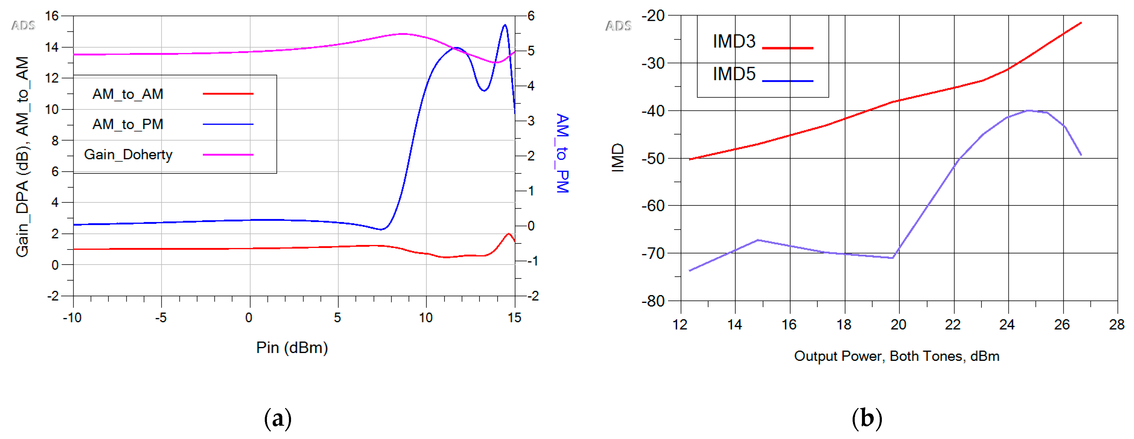
Finally, by increasing the input power level, the nonlinear characteristic of the AM/AM and AM/PM distortion of the DPA are examined, as shown in
Figure 11a. It can be noticed that the output amplitude is distorted at the load modulation regime, where odd components are present. The AM/PM effect caused by the device’s nonlinearity contributes to the IMD products and increases the phase distortion on the output signal. The predistortion linearizer can mitigate these distortions.
Figure 11b simulates MD3 and IMD5 under the two excitations centered at a frequency of 26 GHz. The designed DPA is tested with a 10 MHz deviation of the two-tone signal.
Figure 11b shows the simulated third-order intermodulation distortion (IMD3) and the fifth-order intermodulation distortion (IMD5) products derived from the device’s nonlinearity. The Class-C bias condition of the peaking PA affects the IMD3 and IMD5 of the DPA in the high-power region. Up to the 27 dBm output power range, the IMD3 and IMD5 are less than −20 dBc, which reflects reasonable linearity at two differently biased PAs with tone spacing.
The performances of the recently published mm-wave GaAs pHEMT MMIC DPAs in the literature are compared with the proposed two-stage DPA, and the results are summarized in
Table 1. The presented mobile handset DPA consumes 4 V supply voltage and provides superior broadband performance among other fully integrated counterparts.


 ,
, 


