Article

Broadband Millimeter-Wave 5G Power Amplifier Design in 22 nm CMOS FD-SOI and 40 nm GaN HEMT

1
Department of Electrical and Computer Engineering, Texas Tech University, Lubbock, TX 79409, USA
2
Noise Figure Research, Renton, WA 98057, USA
*
Author to whom correspondence should be addressed.
Electronics 2022, 11(5), 683; https://doi.org/10.3390/electronics11050683
Submission received: 25 January 2022 / Revised: 15 February 2022 / Accepted: 16 February 2022 / Published: 23 February 2022
(This article belongs to the Special Issue Power Amplifier for Wireless Communication)

Abstract

:
Three millimeter-wave (mm-Wave) power amplifiers (PAs) that cover the key 5G FR2 band of 24.25 to 43.5 GHz are designed in two different state-of-the-art device technologies and are presented in this work. First, a single-ended broadband PA that employs a third-order input matching network is designed in a 40 nm GaN/SiC HEMT (High Electron Mobility Transistor) technology. Good agreement between the measurement and post-layout parasitic extracted (PEX) electromagnetic (EM) simulation data is observed, and it achieves a measured 3-dB BW (bandwidth) of 18.0–40.3 GHz and >20% maximum PAE (power-added-efficiency) across the entire 20–44 GHz band. Expanding upon this measured design, a differential broadband GaN PA that utilizes neutralization capacitors is designed, laid out, and EM simulated. Simulation results indicate that this PA achieves 3-dB BW 20.1–44.3 GHz and maximum PAE > 23% across this range. Finally, a broadband mm-Wave differential CMOS PA using a cascode topology with RC feedback and neutralization capacitors is designed in a 22 nm FD-SOI (fully depleted silicon-on-insulator) CMOS technology. This PA achieves an outstanding measured 3-dB BW of 19.1–46.5 GHz and >12.5% maximum PAE across the entire frequency band. This CMOS PA as well as the single-ended GaN PA are tested with 256-QAM-modulated 5G NR signals with an instantaneous signal BW of 50/100/400/9 × 100 MHz at a PAPR (peak-to-average-power ratio) of 8 dB. The data exhibit impressive linearity vs. POUT trade-off and useful insights on CMOS vs. GaN PA linearity degradation against an increasing BW for potential mm-Wave 5G applications.

1. Introduction

5G eMBB (enhanced Mobile Broadband) applications target 10 Gb/s download speeds and ×100 more wireless connected devices compared to 4G for mMTC (massive machine type communication), and sub-1 mS latency time for UR/LL (ultra-reliable low latency), mMTC [1]. However, to achieve all these goals for broadband operation, it is necessary to move up from the sub-6 GHz FR1 band to the millimeter-wave (mm-Wave) 5G FR2 band where more of the frequency spectrum is available. The power-added efficiency (PAE) and linearity for electronics and especially the power amplifiers (PAs) will be considerably lower in the FR2 band due to its much higher operation frequency and thus higher loss compared to the FR1 band. Because the PA can be the most power-hungry component in front-end modules (FEM), the mm-Wave PA is a critical barrier to overcome for low-power 5G circuits and systems in the FR2 band. For example, we may have to use more complicated mm-Wave phased array systems to achieve 3-D beamsteering in the 5G FR2 band, due to higher path loss at these frequencies. With more FEMs needed for phased arrays, inefficient systems will generate added heat and reliability issues. Additionally, to potentially reduce the total number of FEMs needed to cover the entire ~20 GHz BW (bandwidth) of the mm-Wave 5G FR2 band, it would be very attractive to have highly efficient and broadband mm-Wave PAs. In 5G user equipment (UE) and femto/picocells, the PA’s POUT will only need to be in the sub-Watt range of less than 20 dBm [2]. Thus, in this proposed work, we will investigate the design of mm-Wave PAs with excellent broadband peak PAE and good linearity that can cover the key 5G FR2 band in two state-of-the-art technologies that target this medium output power range.
Output power, frequency performance, size, and cost are inherent characteristics in every technology. For instance, even though devices in smaller technology nodes can generally achieve higher fT, and thus better frequency performance, they have limited output power due to lower breakdown voltage (i.e., Johnson’s Limit [3]) compared to larger technology nodes. Additionally, wide-bandgap III-V technologies tend to have higher breakdown voltages and larger carrier transport mobilities compared to silicon technologies. Thanks to the thicker process layers and their semi-insulating substrates, III-V technologies also provide better low-loss on-chip passives, which is crucial for the high Q needed to achieve great power efficiencies and on-chip EM structures (e.g., baluns). Thus, silicon designers must devise ways to work around these intrinsic device limitations to provide power-efficient and robust designs comparable to those of best III-V technologies. However, silicon-based technologies offer more integrability and significantly lower costs, allowing for switches, LNA, and PA to easily coexist in the same die, providing the possibility for a one-chip solution and reducing the need for SiP (system-in-package) or heterogeneous integration.
The GaN technology used in this work is HRL Laboratories’ T3 40 nm GaN HEMT (High Electron Mobility Transistor) technology on a SiC substrate, which achieves VBR of 50 V, fT of 220 GHz and fMAX of 400 GHz with a knee voltage of ~2 V, and ID,MAX of ~1.6 A/mm [4]. This technology will be used in a single-ended PA design (i.e., GaN PA #1) as well as a differential design (i.e., GaN PA #2).
This work will also use Global Foundries’ 22FDX technology, which is a 22 nm FD-SOI (fully depleted SOI) CMOS process to design a differential cascode mm-Wave broadband PA. Devices in this technology achieve lower off-state leakage current due to the buried oxide layer and a fully depleted channel [5]. Our design uses SLVTNFET (i.e., super low threshold voltage NFET), which can achieve a peak fT of ~350 GHz and a peak fMAX of ~370 GHz in the smallest device. The 22FDX technology also enables back-gate biasing, allowing us to change the NFET threshold voltage (VT) by back-gate controls to possibly adjust for VT variation (from poly CD and short-channel effects), and can thus improve the yield for nm-CMOS and possibly improve linearity as well [6].
Figure 1 shows the simulated fT and fMAX of the 40 nm GaN HEMT and 22 nm CMOS FD-SOI devices used in our mm-Wave PA designs. Although the 22FDX PDK (process design kit) offers layouts up to mid-level metal layers, the parasitic up to the top metal layer is extracted using Calibre xACT R + C + CC extraction [7]. Here fT and fMAX are extrapolated when H21 (small-signal current gain) and the value of GMAX (maximum transducer power gain) are equal to unity, respectively (note: G m a x = | S 21 S 12 | ( K K 2 1 ) ). For a fixed current density, it is clear from Figure 1b that fMAX of the GaN device is much higher than those of the CMOS (by ~×2), suggesting it may be more suitable for low-power operations, even though Figure 1a shows CMOS can reach about the same fMAX as the GaN device at a higher bias current (i.e., >10 mA).
In each of the two technologies, we have designed a differential PA, using neutralization capacitors to increase the maximum stable power gain (MSG) and reverse isolation. This technique has been explored in many previous works [8,9] and thus will not be discussed in detail here but we will instead just provide a brief review. From the MSG equation and the small-signal model of a MOSFET, for a differential pair with a neutralization capacitor Cx, Equation (1) can be derived where the parasitic gate to drain capacitance, Cgd, can be reduced by adding the neutralization capacitor Cx, and thus can increase the MSG of a differential amplifier [8,9].
G S = | Y 21 | | Y 12 | = g m 2 ω 2 ( C g d C x ) 2 + 1

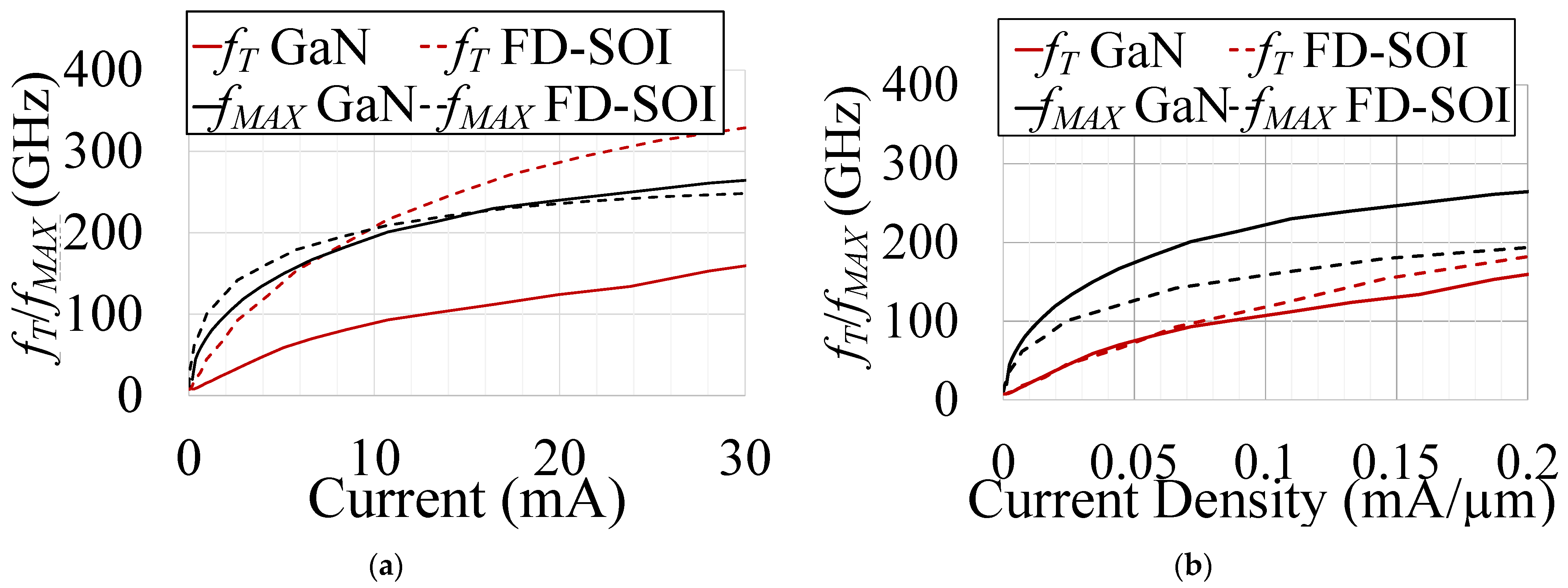
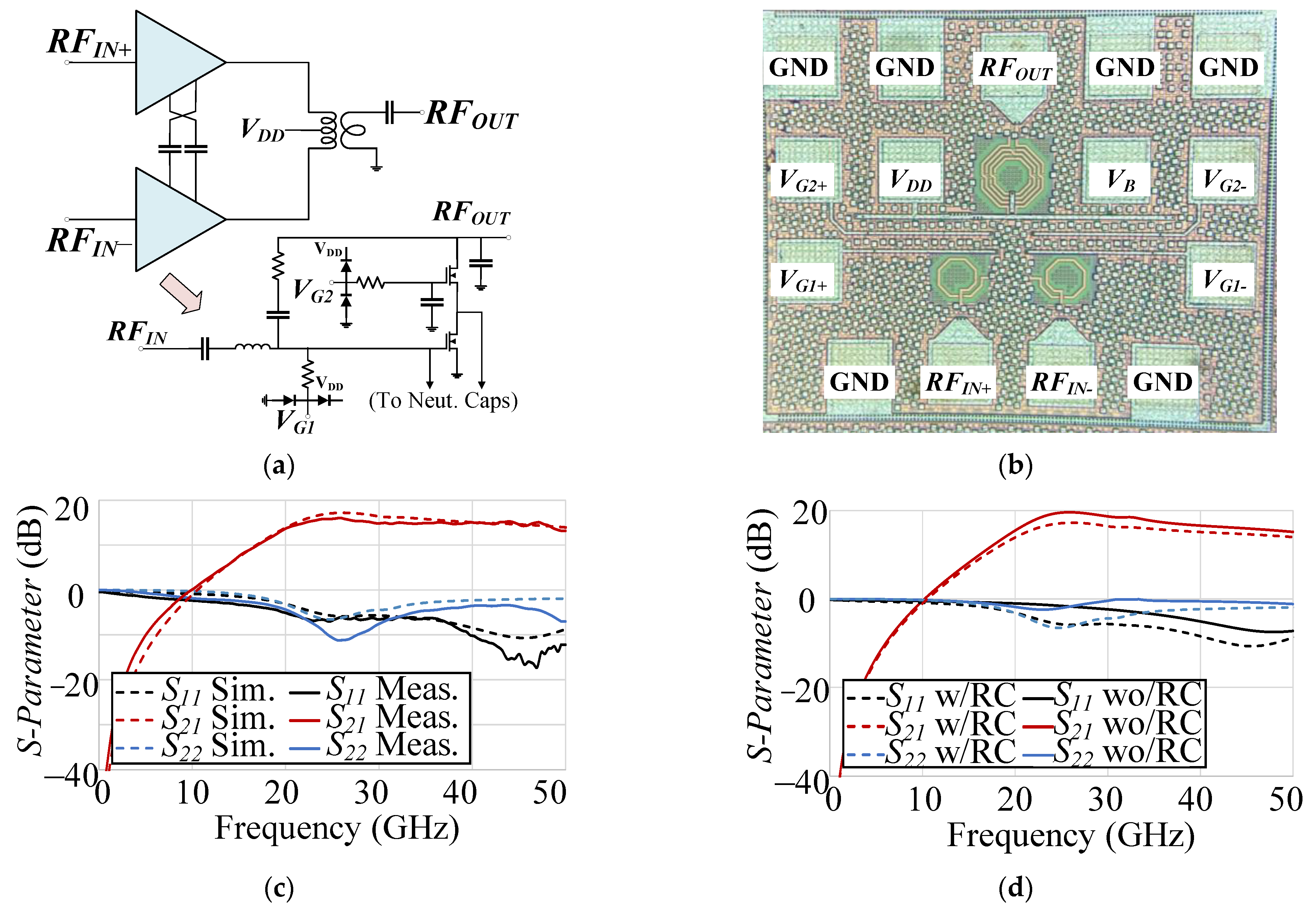
2. Design Methodology

Different design techniques and methodologies will be explored using these two technologies to achieve a very broad BW with good PAE performance. For example, a high-order input-matching network (3rd-order) has been used for the GaN technology, which improves the BW by adding additional zeros and poles to the PA’s transfer function. In the CMOS PA, RC feedback is utilized, which improves the BW with a small sacrifice to the maximum gain with feedback and by also adding an additional pole to the transfer function.
Load-pull simulations are performed in both technologies to help design these broadband PAs. For broadband operation, it is desirable to have the device’s optimum load for PAE near 50 Ω so that minimal impedance transformation is needed, reducing the number of lossy components to realize the narrow-band impedance transformation. In addition, it would be great to have a very small reactance at the device’s optimum load to minimize frequency dependence in the impedance to achieve good broadband performance.
Using load-pull simulations on several GaN devices of different sizes with measurement-based models performed in the Cadence AWR (Applied Wave Research) design environment, a 4 × 37.5 µm device is chosen for a good trade-off of high PAE and gain. The fundamental load-pull simulations for maximum PAE circles for the 4 × 37.5 µm device are shown in Figure 2 for VDD = 4/6/12 V at 24 GHz and 37 GHz, respectively. Not only is the PAE lower for a 12 V supply compared to a 4/6 V supply, but the optimum load also has higher reactance, and thus may make it more difficult to achieve broadband results with 12 V operation. First, a single-ended PA is designed with input and output matching networks, RF choke, and 1 pF bypass capacitors all on-chip. Using the load-pull simulations, the output matching is designed using only 3 matching components (including the RF choke) to minimize the loss for high PAE. To achieve good broadband S11 and increase the usable gain bandwidth, a 3rd-order input matching network is utilized (see Figure 4). The PA is biased at class A/B mode for a good trade-off of linearity and PAE. After this single-ended PA was designed and tested, a differential version was designed where neutralization capacitors are added to increase the gain, as will be discussed later.
In the CMOS FD-SOI technology, PAE and POUT load-pull simulations are performed in Cadence Spectre. First, these simulations are performed on a single-ended cascode device pair with parasitic elements again extracted up to the top metal layer as shown in the schematic in Figure 3a. These simulations are performed at around OP1dB and indicate that at 24/37 GHz, the cascode device can achieve maximum PAE of 35.0%/33.0% and POUT,MAX of 11.9/11.8 dBm, respectively. Load-pulls simulations are then also performed on a differential cascode device pair with small neutralization capacitors (see Figure 3d), and they achieve maximum PAE and POUT,MAX values of 33.5%/32.5% and 14.8/14.5 dBm at 24/37 GHz, respectively (still at around OP1dB). The optimal load impedance of maximum PAE and POUT,MAX can occur close to each other on the Smith Chart as indicated by the load-pull simulations, and thus, these devices can almost be simultaneously optimized for both PAE and output power. Additionally, load-pull simulations suggest that these devices could achieve broadband performance as the optimal load does not move far from 24 to 37 GHz.
As discussed previously, this differential PA design utilizes neutralization capacitors for gain and reserve isolation improvement. An RC feedback path is also added to improve the BW of this design. On-chip baluns and transformers are offered in this mature PDK, and this design utilizes one of these center-tapped on-chip baluns to convert the differential output to a single-ended RFOUT, for output matching and feeding the VDD. Due to this small technology node, ESD double diodes are added to all the gate pads to protect the PA from ESD events. The cascode device pair presented here is not quite designed in a classical cascode topology, as a gate capacitor of ~450 fF is used at the top cascode device in this work instead of using a larger capacitor to make a CG (common-gate) device’s gate a classic RF ground. This choice of “hybrid” design between a stacked vs. a cascode topology can still effectively mitigate the breakdown concerns by sharing the total voltage swing of the output of the PA across the bottom CS (common-source) and the top cascode device [10].

3. Results

For all of the measurements shown in this work, the RF input is probed and the DC voltages are provided by gold wire-bonded pads to a custom PCB (printed circuit board), where more bypass capacitors are added for better stability on all DC traces. Later in this paper, modulated 5G NR data will be used as the RF input signal, and the PAs are measured with the state-of-the-art mm-Wave PXIE (PCI express extensions for instrumentation) system by National Instruments (NI), which can produce modulated 5G NR signals of up to 1 GHz BW and up to 44 GHz [11]. In the following discussions, besides the 3-dB BW conventionally used, the BW of these PAs is often also compared by the absolute BW, defined as 2 ( f H f L f H + f L ) [12] where fH is the upper frequency and fL is the lower frequency of the 3-dB BW.

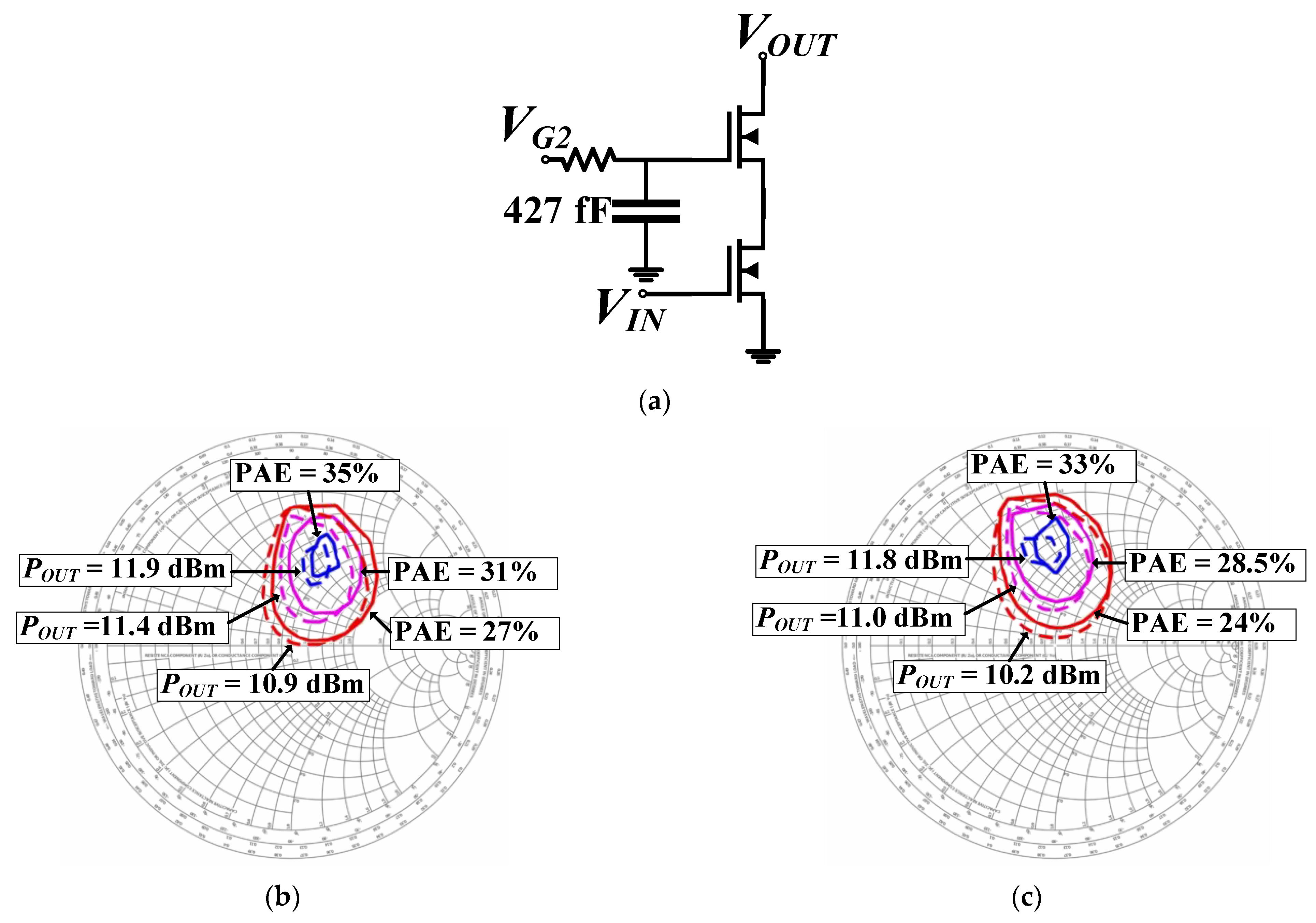
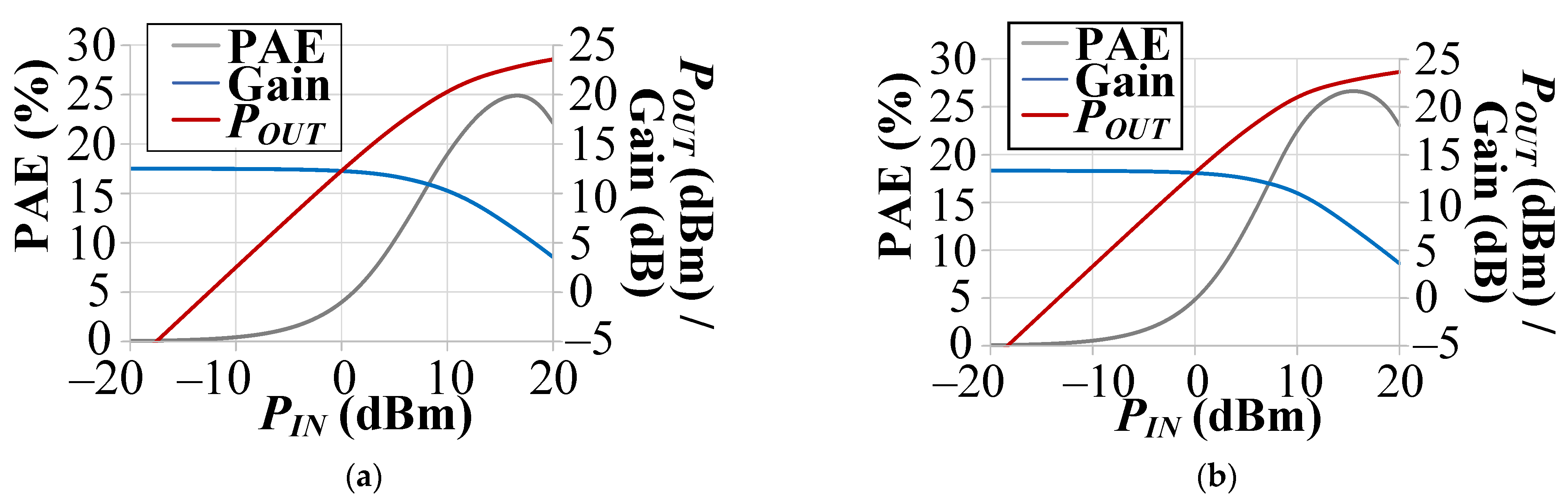
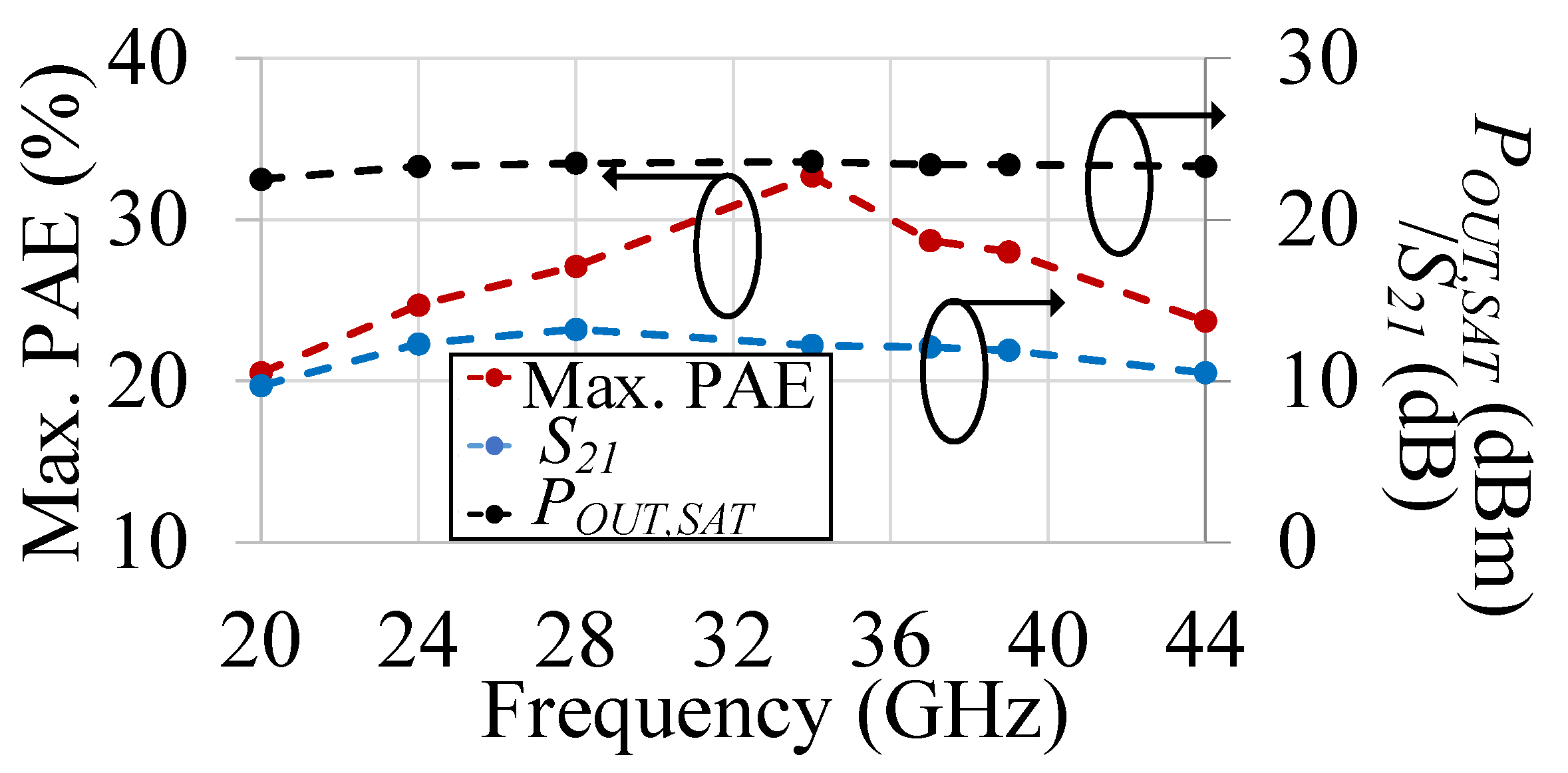
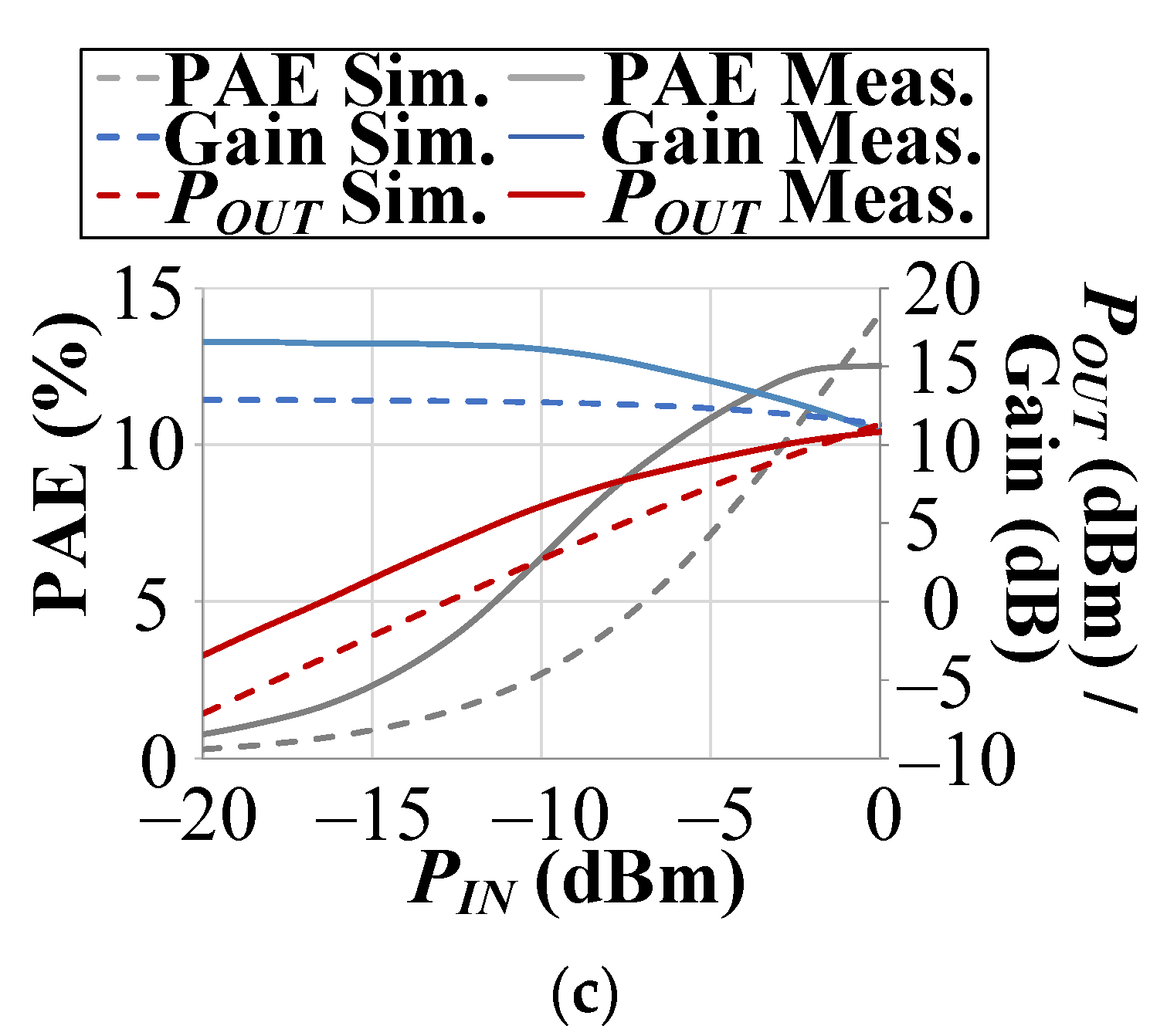
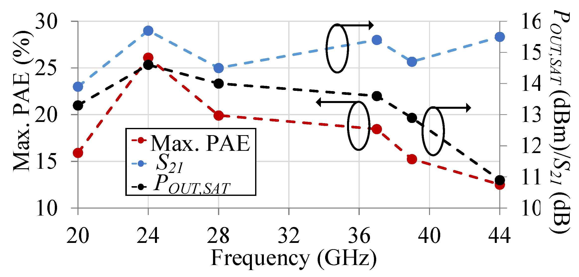
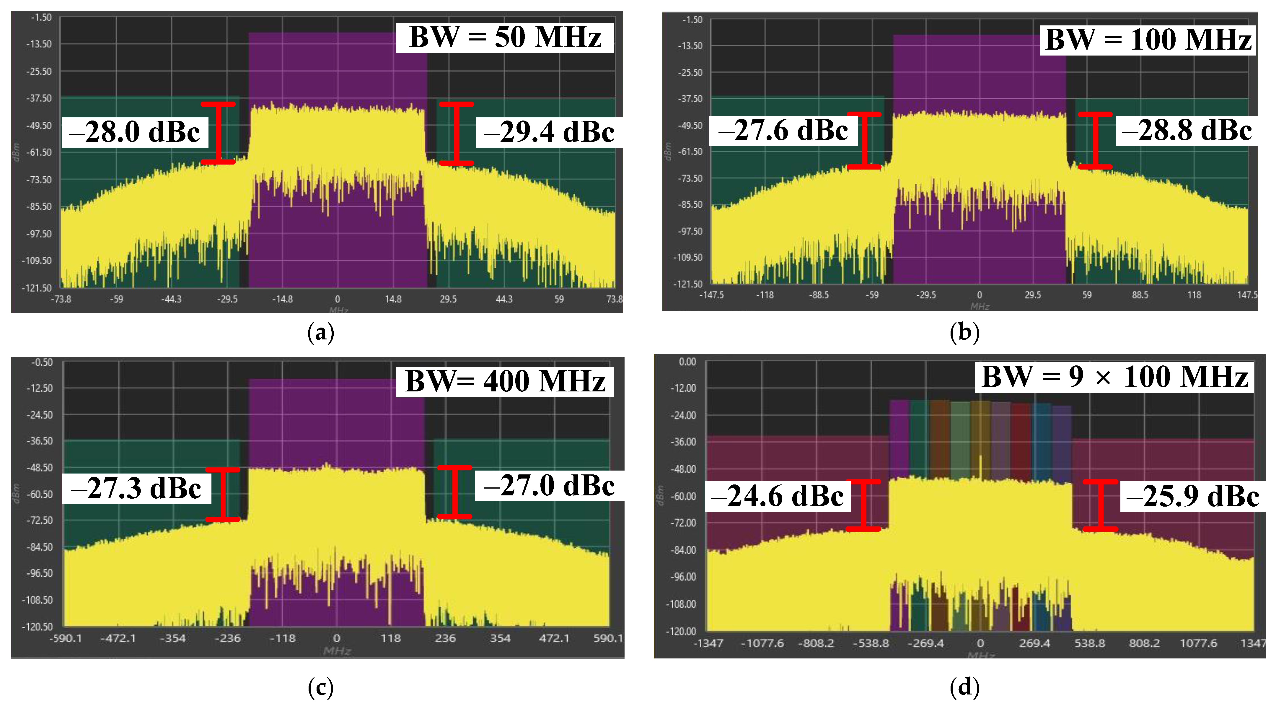
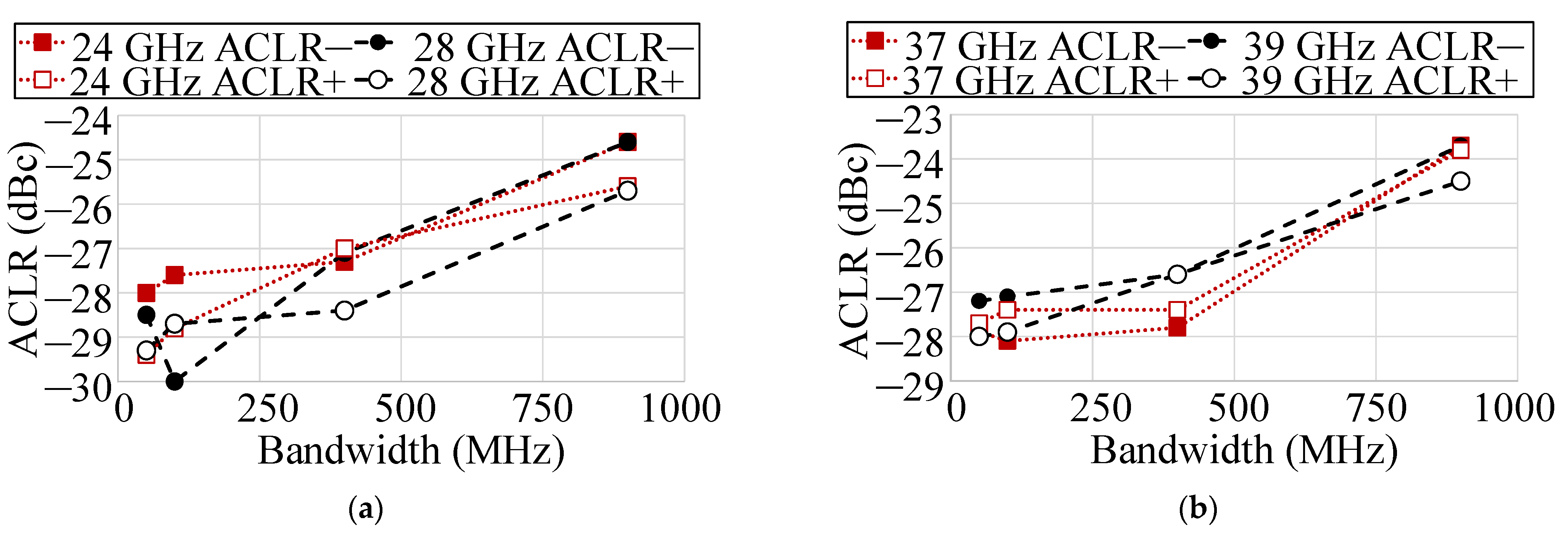
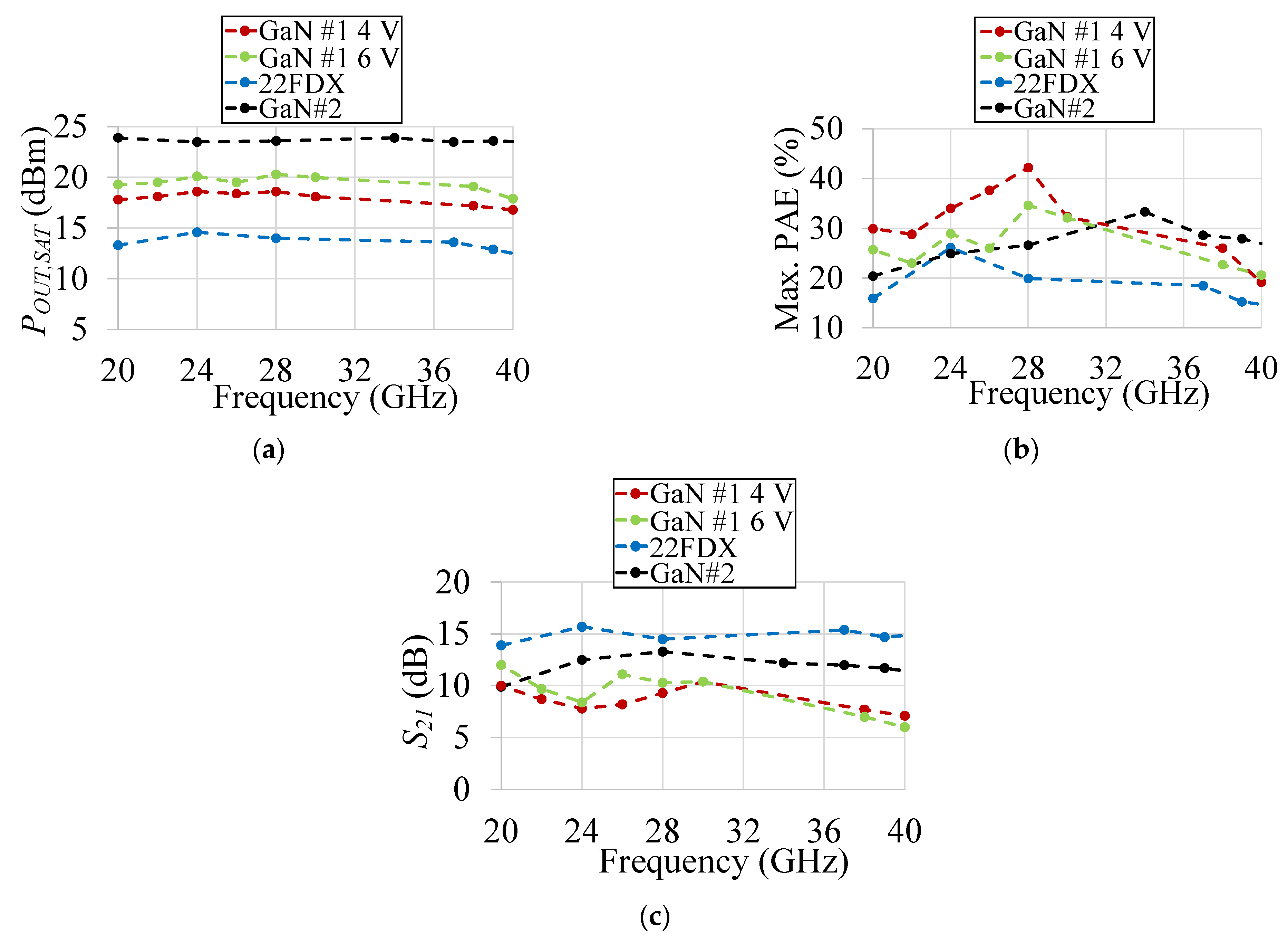
3.1. Single-Ended GaN (GaN #1) PA Measurement Results

Figure 4 shows the final schematic of the single-ended broadband GaN PA as well as the S-Parameter measurement vs. post-layout EM simulation. The EM simulations for the HRL GaN PDK are performed using Cadence’s AXIEM in AWR to include all layout parasitic elements. This PA achieves maximum S21 of 12.5 dB and a small-signal 3-dB BW of 18–38.7 GHz (absolute BW = 73.0%) at VDD = 6 V, and S21 = 10.3 dB with BW = 18–40.3 GHz (or an absolute BW = 76.5%) at VDD = 4 V. Although not plotted here, S-Parameter measurements with VDD = 12 V shown in [13] achieved maximum S21 = 13.0 dB with BW = 18.3–32.7 GHz (absolute BW = 56.5%). Thus, as the load-pull EM simulations had suggested, lowering the drain voltage makes this design more broadband. The S21 modeling at VDD = 4 V is not as accurate vs. VDD = 6 V, which may be due to the 4 V model being constructed from extrapolation whereas the 6 V models are directly from measurements. However, we do see that the S11 and S22 do match well with simulations for both supply voltages of 4 V and 6 V.
The large-signal measurement results vs. post-layout EM simulations are shown in Figure 5 for VDD = 4 and 6 V at 24, 28, and 44 GHz. This PA achieves a maximum PAE/PSAT of 34.0%/18.6 dBm at 24 GHz, 42.1%/18.6 dBm at 28 GHz, and 21.6%/17.8 dBm at 44 GHz. With a 6 V supply, there is once again good agreement between the measurement and simulation data, and the PA achieves maximum PAE/PSAT of 28.9%/20.1 dBm at 24 GHz, 34.6%/20.3 dBm at 28 GHz, and 19.1%/19.3 dBm at 44 GHz. Figure 6 shows the measured POUT,SAT and maximum PAE plotted across the frequency, which highlights the broadband performance of this PA as it is able to maintain greater than ~20% PAE across the entire band of 18–40 GHz for VDD = 4 V and greater than 14% PAE with VDD = 6 V. The peak PAE for VDD = 4 V is much higher at above 42% at 28 GHz.
PA Linearity is then tested with 50, 100, 400, and 9 × 100 MHz 256-QAM-modulated 5G NR inputs at PAPR (peak-to-average-power ratio) = 8.0 dB at 24 GHz and VDD = 4 V (Figure 7). With POUT,AVE = ~11 dBm, this PA achieves ACLR −/+ (adjacent channel leakage ratio) of −27.6/−27.0 dBc with BW = 50 MHz (PAEAVE = 13.3%), −27.4/−27.2 dBc with BW = 100 MHz (PAEAVE = 12.1%), −26.7/−26.8 dBc with BW = 400 MHz (PAEAVE = 11.8%), and −25.5/−26.0 dBc with BW = 9 × 100 MHz (PAEAVE = 12.0%). The signal BW is varied from 50–900 MHz at 24, 28, 37, and 39 GHz, and the measured ACLR vs. BW is plotted in Figure 8 all at POUT,AVE ~11 dBm when VDD = 4 V, and POUT,AVE = ~12 dBm with VDD = 6 V. Figure 8 shows that there is not a significant degradation in the PA linearity increasing the 5G NR signal BW from 50 MHz to 9 × 100 MHz at 28, 37, and 39 GHz, and only a slight degradation (~2 dBc) in the measured ACLR at 24 GHz for both VDD = 4 V and 6 V. Additionally, there is minimal degradation on the linear output power, increasing from 24/28 GHz to 37/39 GHz.

3.2. Differential GaN (GaN #2) PA PEX EM Simulation Results

The single-ended broadband GaN PA discussed above was then used to form a differential broadband mm-Wave 5G PA as shown in Figure 9, where the CS topology is used and the neutralization capacitors are added for improved MSG and for comparison purposes against a reasonably similar differential FD-SOI CMOS PA that will be presented later in this paper. Additional RC traps were added at the gates of these GaN transistors to further stabilize the PA, and this differential design has an area of 1.94 mm2 (with pads), slightly larger than the 1.85 mm2 area of the single-ended design. PEX EM simulations indicate that this differential GaN PA achieves a maximum S21 of 13.4 dB, with a 3-dB BW from 20.1–44.3 GHz (or an absolute BW of 75.2%) at VDD = 6 V, of which the BW is comparable to the single-ended GaN #1 design, but with a significantly higher gain and POUT.
The large-signal EM simulation results for this differential GaN PA are shown in Figure 10, which indicates that this PA can achieve a maximum PAE of 24.9%/26.6%/23.3% and POUT,SAT of 23.5/23.6/23.3 dBm at 24/28/44 GHz. Figure 11 shows the broadband nature of this PA, as it is able to achieve >20% maximum PAE across the 20–44 GHz band, and has a very high simulated 1-dB POUT,SAT BW and also POUT,SAT larger than ~23 dBm in the 5G FR2 band of interest. Compared to the measured GaN #1 PA, it achieves a similar maximum PAE, while having ~3 dB greater POUT,SAT than the single-ended design. We will discuss another broadband differential mm-Wave 5G PA designed in 22 nm FD-SOI CMOS next.

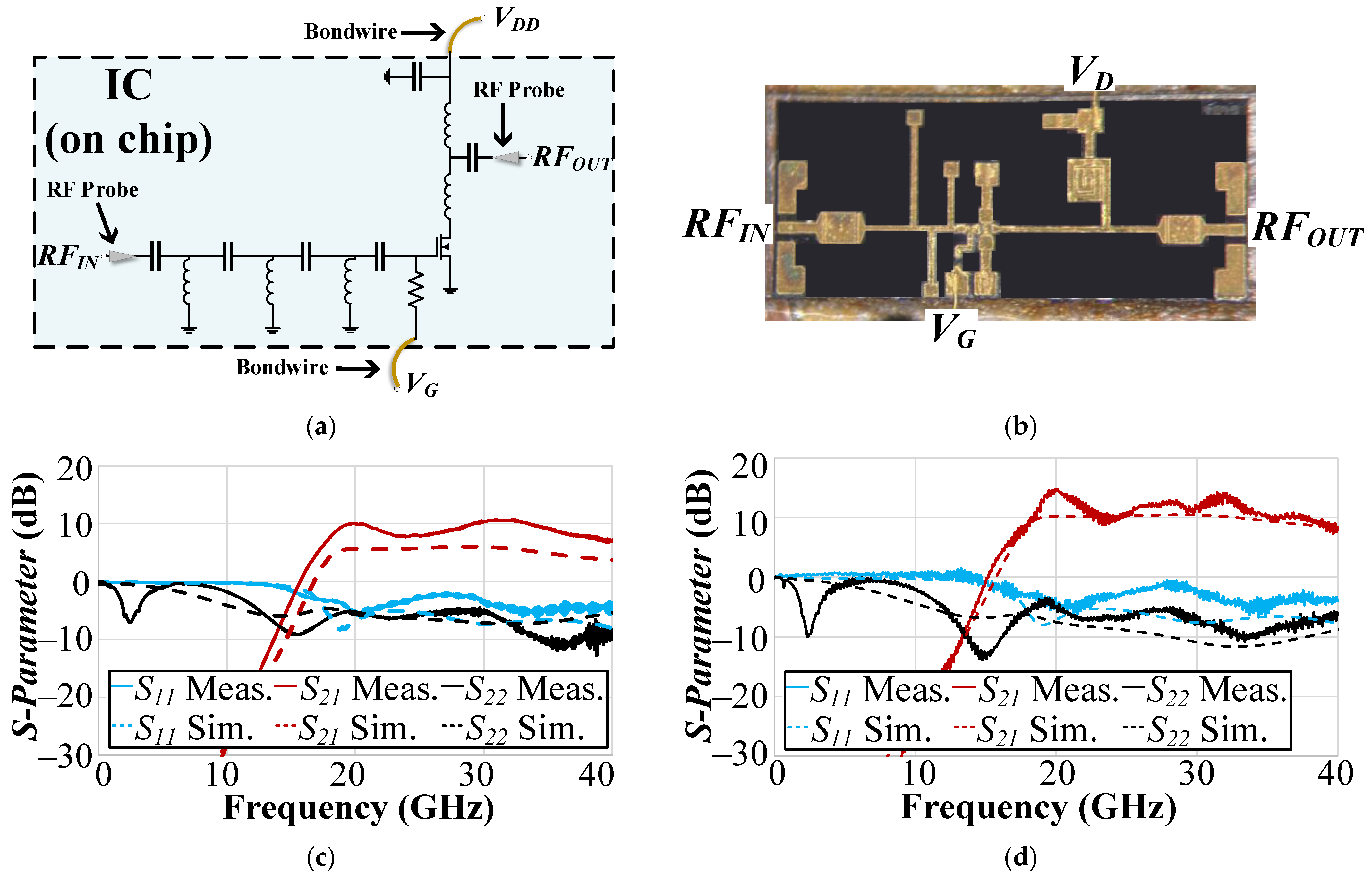
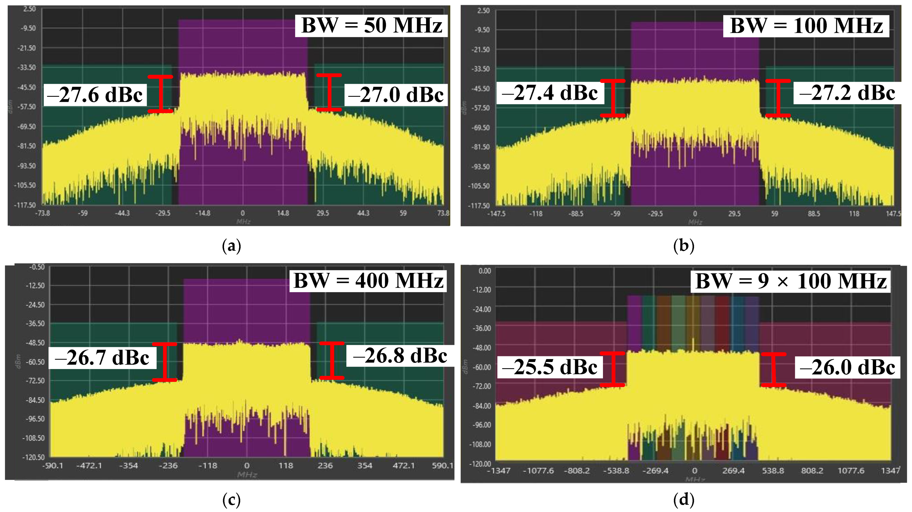
3.3. Differential Cascode CMOS PA Measurement Results

Figure 12 presents the schematic of the differential cascode CMOS PA designed in the 22FDX technology and the small-signal S-parameter measurement data compared to post-layout PEX simulations of this PA. Layout parasitic elements for this design were extracted using Mentor Graphic’s Calibre R + C + CC extraction. Small-signal measurement data agree well with the PEX simulations, exhibiting excellent broadband performance. PEX simulations achieve a maximum S21 small-signal gain of 17.4 dB with 3-dB BW of 20.5–47.4 GHz (or an absolute BW of 79.2%), while measurement achieves a 3-dB BW of 19.1–46.5 GHz and a maximum S21 = 16.4 dB (absolute BW of 83.5%). The RC feedback network allows for adequate input matching with S11 < −5.5 dB across the entire ~27 GHz band in both simulation and measurement values. Thus, measurement data display virtually no degradation on the targeted small-signal broadband BW to cover the entire key 5G FR2 band of 24.25–43.5 GHz, as indicated by the PEX simulations, and only minimal degradation in measured vs. the simulated values of small-signal gain.
The effect of the RC feedback on this differential CMOS SOI PA design is also simulated here in post-layout PEX simulations in Figure 12d, where the original design is compared to the same design with the only change being that the RC feedback is removed (and the PA layout is re-extracted and re-simulated). Here, it shows that the overall gain is reduced by ~2 dB when RC feedback is added, as this PA without the RC feedback achieves a maximum S21 = 19.6 dB. However, the BW is increased when RC feedback is added, as, without it, the 3-dB BW decreases to 20.9–39.6 GHz (or an absolute BW of 61.8%). Thus, the absolute BW is degraded by ~15% without the RC feedback, and the input/output matching worsened considerably as well.
The large-signal measured data vs. PEX simulation results at 24/28/44 GHz are shown in Figure 13, where degradation in the large-signal measurement data from simulations is seen, likely due to inaccuracies in the large-signal transistor modeling. These figures show that at 44 GHz, the measured gain is 3 dB higher than those of the PEX EM simulations. The measured gain values are usually reduced by 1–2 dBs from the simulated data at 24–39 GHz, while at 24/28/44 GHz this broadband PA achieves measured OP1dB of 11.5/9.2/7.4 dBm with PAE @OP1dB of 18.6%/11.2%/9.3%, PSAT of 14.6/14.0/10.9 dBm, and maximum PAE of 26.1%/19.9%/12.5 %, respectively.
Figure 14 plots the measured maximum PAE, S21, and POUT,SAT vs. the frequency from 20–44 GHz, which shows this PA maintains a maximum PAE ≥ 12.5% and POUT,SAT ≥ 11 dBm across this frequency range. It achieves a maximum PAE ≥ 15.1% and POUT,SAT ≥ 12.9 dBm across 24–39 GHz, highlighting the broadband performance of this CMOS PA.
As has been conducted with GaN design #1, this CMOS PA’s linearity is tested with 50/100/400/9 × 100 MHz 256-QAM NR input signals with the same PAPR = 8.0 dB and same NI PXI equipment at 24 GHz, and the PA output spectra are shown in Figure 15. With the same output power of POUT,AVE = ~7 dBm, at the instantaneous signal BW = 50 MHz this PA achieves an ACLR −/+ of −28.0/−29.4 dBc (PAEAVE = 7.3%), with BW = 100 MHz, −27.6/−28.8 dBc (PAEAVE = 7.0%), with BW = 400 MHz, −27.3/−27.0 dBc (PAEAVE = 7.7%), and with BW = 9 × 100 MHz, −24.6/−25.9 dBc (PAEAVE = 8.1%).
Similarly, this PA’s linearity is also tested at 50–900 MHz BW at several other frequencies in the 5G FR2 band. When varying the BW of a 256-QAM 5G NR signal (PAPR = 8 dB) at 24 GHz and 28 GHz, the POUT,AVE is about 7 dBm, and at 37 GHz and 39 GHz, POUT,AVE is approximately ~6 dBm. Figure 16 also shows interesting ACLR measurement data vs. signal BW. When the BW is increased from 50 MHz to 100 MHz, the linearity is not affected much, but when increasing it from 100 MHz to 400 MHz, the PA’s linearity is degraded by a small but noticeable amount of ~1–3 dB. Then, increasing the BW from 400 MHz to 9 × 100 MHz, the linearity becomes further degraded by an additional ~2 dB at all frequencies measured. Although, this CMOS PA’s linear output power only degrades by ~1 dB when its operating frequencies change from 24/28 GHz to 37/39 GHz.

4. Discussion

In the previous sections, three different PAs from two different technologies were presented. Typically, GaN is used for higher-power applications, but the designs in this work are all targeted to perform in the sub-Watt range. Small-signal measurements matched well with PEX simulations for both GaN #1 and the CMOS PA. However, large-signal measurement results did not match well for the CMOS PA, whereas large-signal measurements for the GaN #1 for VDD = 6 V matched the simulation results rather well. Although measurements have not been taken on GaN #2 as this design is in the process of being fabricated, measurements on GaN #1 showed good agreement with EM simulations for VDD = 6 V and thus will be compared to the other PAs here with VDD = 6 V. Although the 22 nm FD-SOI CMOS PA used several power-performance improvement techniques (i.e., cascode and differential operation), the comparison of the three PAs in Figure 17 and Table 1 show that the POUT,SAT is significantly higher for the broadband single-ended or differential GaN PAs vs. the CMOS PA. This could be explained by the superior breakdown performance of GaN over the CMOS technologies, enabling larger output voltage swings per device. GaN #2 and the 22FDX PA both used a differential topology and have similar gain, and the PAE as well as POUT appears superior for the GaN #2 PA vs. those of the CMOS-SOI PA. However, the broadband differential CMOS FD-SOI PA is much smaller than the GaN PAs in die size, with slightly higher power gain (but much lower POUT,SAT vs. GaN PAs), and it also includes an output balun, highlighting the excellent integrability of this CMOS technology. Using aggressive 256 QAM-modulated 5G NR input waveforms, great design insights can be gained from the measured ACLR vs. frequency on the signal BW vs. linearity and POUT,Linear for these two device technologies. When the signal BW is increased from 50 MHz to 900 MHz, the ACLR is degraded by ~2 dBc for GaN #1 for both VDD = 4 V and 6 V at 24 GHz and virtually does not degrade at 28, 37, and 39 GHz. However, for the CMOS PA, the ACLR degrades with this broadened signal BW by ~4 dBc at all the carrier frequencies tested. Thus, this 40 nm GaN/SiC technology appears to have better linearity against very wide GHz 256QAM-modulated 5G NR signals across the FR2 band, and offers significantly higher POUT,Linear and POUT,SAT than the 22FDX CMOS technology. However, as we do not have measured POUT,Linear data for the differential GaN #2 yet, we could not ascertain if the superior POUT,Linear of broadband GaN PAs is mainly due to the device technology difference (i.e., GaN or FD-SOI), the cascode vs. common-source topology difference, the single-ended vs. differential topology difference, or something else (such as the output balun and/or matching details). Therefore, more detailed studies with additional measurement data are required to illuminate and clarify this important point in the future.
Our GaN PAs are compared to other state-of-the-art medium-power broadband mm-Wave 5G PAs in Table 2, as well as against some GaN PAs in the literature with higher power values, as most available mm-Wave GaN PAs in the literature are targeted at higher-power applications without optimizing for high PA linearity. Although GaN #2 still requires measurement results for validation, Table 2 shows that both of our GaN PAs achieve some of the best small-signal 3-dB BW as well as good PAE. Additionally, the GaN #1 design achieved excellent measured BW and good linearity with aggressive 5G NR signal modulation and instantaneous ~1 GHz signal BW, which have not been reported in prior medium-power mm-Wave GaN PAs [13]. Depending on the application, this GaN technology allows for the VDD to be varied from 12 V to 4 V to achieve the optimal trade-off of PAE and output power. Although operating this PA at VDD = 4 V reduces POUT with an increase in cost, being able to vary the supply voltage like this is not as easily feasible for silicon-based stacked broadband mm-Wave PAs. Thus, we conclude our GaN #1 PA exhibits excellent 3-dB BW, peak and linear PAE, and POUT,Linear with stringent 256-QAM modulation and a rather large instantaneous signal BW of 9 × 100 MHz across the key 5G FR2 band; it is among the best broadband linear mm-Wave medium-power PAs in the literature.
Our 22 nm broadband CMOS SOI PA vs. other state-of-the-art broadband medium-power mm-Wave PAs is also shown in Table 2. Our CMOS PA achieves the best small-signal 3-dB BW in the literature, and it has obtained good broadband linearity/PAELINEAR. It is also tested with the most stringent modulation (i.e., 256-QAM) and has a rather large instantaneous signal BW (i.e., 400 MHz and 9 × 100 MHz).

5. Conclusions

This work presented three different, very broadband, linear, and efficient PAs that can operate over the entire key mm-Wave 5G FR2 band of 24–44 GHz in two different state-of-the-art semiconductor IC technologies. Using a third-order input-matching network, a broadband, single-ended 40 nm GaN PA was designed (i.e., GaN PA #1), achieving excellent performance from 18 to 44 GHz, with the highest measurement maximum PAE/POUT,SAT of 42.1%/18.6 dBm at 28 GHz at VDD = 4 V. Small-signal and large-signal CW measurement data matched EM PEX simulations well, with maximum PAE above ~20% across the entire frequency band. When inserting a 256-QAM 5G NR signal varying in BW from 50 MHz to 9 × 100 MHz at 24, 28, 37, and 39 GHz, there is virtually no degradation in the linearity as measured by ACLR for this GaN #1 PA. This PA is used to design a broadband differential PA with neutralization capacitors in the same GaN technology (i.e., GaN PA #2), which achieves similar PAE and BW in PEX EM simulations as the single-ended version, but with higher ~3 dB gain and higher POUT,SAT, as expected. Finally, a broadband 22 nm FD-SOI CMOS PA was designed, achieving excellent broadband results in the FR2 band with an RC feedback network and differential topology using neutralization capacitors. It achieves a 3-dB BW of 19.1–46.5 GHz and a good maximum PAE of 26.1% at 24 GHz and maintains a maximum PAE above 15.1% across the entire 24–39 GHz. Compared to the GaN #1 PA, increasing the 256-QAM 5G NR signal BW from 50 MHz to 9 × 100 MHz degrades the ACLR linearity of the CMOS PA more, suggesting that the GaN PA may be able to deliver significantly higher POUT,Linear and POUT,SAT than their CMOS counterparts for mm-Wave 5G applications, albeit at a considerably higher cost with a lower level of monolithic integration.

Author Contributions

Conceptualization, J.M. and D.Y.C.L.; methodology, J.M. and D.Y.C.L.; validation, J.M. and D.Y.C.L.; formal analysis, J.M.; investigation, J.M.; resources, D.Y.C.L. and J.L.; data curation, J.M.; writing—original draft preparation, J.M.; writing—review and editing, J.M. and D.Y.C.L.; visualization, J.M.; supervision, D.Y.C.L.; funding acquisition, D.Y.C.L. All authors have read and agreed to the published version of the manuscript.

Funding

This material is based on research sponsored by the Air Force Research Laboratory (AFRL) and the Defense Advanced Research Projects Agency (DARPA) under Grant Number FA8650-19-1-7902. The US Government is authorized to reproduce and distribute reprints for governmental purposes notwithstanding any copyright notation thereon.

Data Availability Statement

Data contained within this article.

Acknowledgments

The authors would like to thank Clint Sweeney for support in this work. We also sincerely thank the GlobalFoundries (GF) University Program, HRL for tapeout support and training, as well as the TTU Keh-Shew Lu Regents Chair Endowment fund.

Conflicts of Interest

The authors declare no conflict of interest. The funders had no role in the design of the study; in the collection, analyses, or interpretation of data; in the writing of the manuscript, or in the decision to publish the results.

References

  1. Available online: www.3gpp.org/ (accessed on 30 November 2018).
  2. Lie, D.Y.C.; Mayeda, J.C.; Li, Y.; Lopez, J. A Review of 5G Power Amplifier Design at cm-Wave and mm-Wave Frequencies. Wirel. Commun. Mob. Comput. 2018, 2018, 6793814. [Google Scholar] [CrossRef] [Green Version]
  3. Voldman, S.H.; Botula, A.; Hui, D.T.; Juliano, P.A. Silicon Germanium heterojunction bipolar transistor ESD power clamps and the Johnson Limit. In Proceedings of the 2001 Electrical Overstress/Electrostatic Discharge Symposium, Portland, OR, USA, 11–13 September 2001; pp. 324–334. [Google Scholar]
  4. Bowen, S.D.B.R.; Tai, J.; Brown, D.; Grabar, R.; Santos, D.; Magadia, J.; Khalaf, I.; Micovic, M. Reliability Characteristics and Mechanisms of HRL’s T3 GaN Technology. IEEE Trans. Semicond. Manuf. 2017, 30, 1. [Google Scholar] [CrossRef]
  5. Available online: www.globalfoundries.com/technology-solutions/cmos/fdx/22fdx (accessed on 23 October 2021).
  6. Mayeda, J.C.; Tsay, J.; Lie, D.Y.C.; Lopez, J. Effective AM-PM Cancellation with Body Bias for 5G CMOS Power Amplifier Design in 22nm FD-SOI. In Proceedings of the 2019 IEEE International Symposium on Circuits and Systems (ISCAS), Sapporo, Japan, 26–29 May 2019; pp. 1–4. [Google Scholar]
  7. Chow, K.; Relyea, C. Parasitic Extraction Technologies. Siemens Digital Industries Software. 2018. Available online: https://static.sw.cdn.siemens.com/siemens-disw-assets/public/81845/en-US/Siemens-SW-Parasitic-extraction-technologies-for-advanced-WP-81845-C2.pdf (accessed on 24 February 2021).
  8. Asada, H.; Matsushita, K.; Bunsen, K.; Okada, K.; Matsuzawa, A. A 60GHz CMOS power amplifier using capacitive cross-coupling neutralization with 16 % PAE. In Proceedings of the 2011 41st European Microwave Conference, Manchester, UK, 10–13 October 2011; pp. 1115–1118. [Google Scholar]
  9. Chan, W.L.; Long, J.R. 58–65 GHz Neutralized CMOS Power Amplifier with PAE Above 10% at 1-V Supply. IEEE J. Solid-State Circuits 2010, 45, 554–564. [Google Scholar] [CrossRef]
  10. Mayeda, J.C.; Lie, D.Y.C.; Sweeney, C.; Lopez, J. A 19.1–46.5 GHz Broadband Efficient Power Amplifier in 22 nm CMOS FD-SOI for mm-Wave 5G. In Proceedings of the 2022 IEEE International Symposium on Circuits and Systems (ISCAS), Austin, TX, USA, 2022. submitted. [Google Scholar]
  11. National Instruments “Instrument Innovations for mmWave Test”. Available online: https://www.ni.com/en-us/innovations/white-papers/19/instrument-innovations-for-mmwave-test.html (accessed on 24 February 2021).
  12. Stutzman, W.L.; Thiele, G.A. Broadband Antennas. In Antenna Theory and Design, 2nd ed.; John Wiley & Sons, Inc.: New York, NY, USA, 1998. [Google Scholar]
  13. Mayeda, J.C.; Lie, D.Y.C.; Lopez, J. A Highly Efficient 18–40 GHz Linear Power Amplifier in 40-nm GaN for mm-Wave 5G. IEEE Microw. Wirel. Compon. Lett. 2021, 31, 1008–1011. [Google Scholar] [CrossRef]
  14. Chappidi, C.R.; Sengupta, K. A 26-42 GHz Broadband, Back-off Efficient and Vswr Tolerant CMOS Power Amplifier Architecture for 5G Applications. In Proceedings of the 2019 Symposium on VLSI Circuits, Kyoto, Japan, 9–14 June 2019; pp. C22–C23. [Google Scholar]
  15. Estella, N.; Camargo, E.; Schellenberg, J.; Bui, L. High-Efficiency, Ka-band GaN Power Amplifiers. In Proceedings of the 2019 IEEE MTT-S International Microwave Symposium (IMS), Boston, MA, USA, 2–7 June 2019. [Google Scholar]
  16. Chen, Y.; Wu, Y.; Luo, L.; Wang, Q.; Zhang, Y.; Yan, B.; Xu, R.; Xu, Y. Design of 18–40 GHz GaN reactive matching power amplifiers using one-order and two-order synthesised transformer networks. IET Microw. Antennas Propag. 2022, 16, 78. [Google Scholar] [CrossRef]
  17. Qunaj, V.; Reynaert, P. A Compact Ka-Band Transformer-Coupled Power Amplifier for 5G in 0.15 um GaAs. In Proceedings of the 2019 IEEE BiCMOS and Compound semiconductor Integrated Circuits and Technology Symposium (BCICTS), Nashville, TN, USA, 3–6 November 2019; pp. 1–4. [Google Scholar]
  18. Hu, S.; Wang, F.; Wang, H. A 28GHz/37GHz/39GHz Multiband Linear Doherty Power Amplifier for 5G Massive MIMO Applications. In Proceedings of the 2017 IEEE International Solid-State Circuits Conference (ISSCC), San Francisco, CA, USA, 5–9 February 2017; pp. 32–33. [Google Scholar]
  19. Li, T.; Huang, M.; Wang, H. Millimeter-Wave Continuous-Mode Power Amplifier for 5G MIMO Applications. IEEE Trans. Microw. Theory Tech. 2019, 67, 3088–3098. [Google Scholar] [CrossRef]
  20. Wang, F.; Wang, H. An Instantaneously Broadband Ultra-Compact Highly Linear PA with Compensated Distributed-Balun Output Network Achieving >17.8 dBm P1dB and >36.6% PAEP1dB over 24 to 40 GHz and Continuously Supporting 64-/256-QAM 5G NR Signals over 24 to 42 GHz. In Proceedings of the 2020 IEEE International Solid-State Circuits Conference-(ISSCC), San Francisco, CA, USA, 16–20 February 2020; pp. 372–374. [Google Scholar]
Figure 1. Simulated fT and fMAX of the 40 nm GaN HEMT (4 × 37.5 µm) and 22 nm CMOS FD-SOI (2 × 20 µm) PA power transistors with parasitic elements extracted to the top metal layer and plotted vs. (a) bias current (mA); and (b) current density (mA/µm).
Electronics 11 00683 g001
Figure 2. Load-pull simulations of the 4 × 37.5 µm GaN device at (a) 24 GHz and (b) 37 GHz for VDD = 12 V; (c) 24 GHz; and (d) 37 GHz for VDD = 6 V; (e) 24 GHz and (f) 37 GHz for VDD = 4 V all at around OP1dB.
Electronics 11 00683 g002
Figure 3. Load-pull simulations of the (a) single-ended cascode device pair (with a 427 fF cap on the cascode gate) at (b) 24 GHz and (c) 37 GHz; and of the (d) differential cascode device pair with neutralization capacitors at (e) 24 GHz and (f) 37 GHz all at around OP1dB.
Electronics 11 00683 g003aElectronics 11 00683 g003b
Figure 4. (a) Simplified schematics and the (b) micrograph of the broadband single-ended GaN PA (2.1 × 0.88 mm2 with pads) and its S-Parameter EM PEX simulations vs. measurement with (c) VDD = 4 V; and (d) VDD = 6 V.
Electronics 11 00683 g004
Figure 5. Large-signal EM PEX simulation vs. CW measurement of the broadband single-ended GaN PA with VDD = 4 V at (a) 24, (b) 28, and (c) 44 GHz and VDD = 6 V at (d) 24, (e) 28, and (f) 44 GHz.
Electronics 11 00683 g005
Figure 6. Measured maximum PAE, S21 and POUT,SAT vs. frequency of the broadband single-ended GaN PA at (a) VDD = 4 V and (b) VDD = 6 V.
Electronics 11 00683 g006
Figure 7. ACLR measurements of the broadband single-ended GaN PA at 24 GHz using a (a) 50 MHz, (b) 100 MHz, (c) 400 MHz, and (d) 9 × 100 MHz 256-QAM 5G NR signal with PAPR = 8 dB.
Electronics 11 00683 g007
Figure 8. Measured ACLR+/ACLR- vs. 5G NR instantaneous signal BW (PAPR = 8 dB) for the broadband single-ended GaN PA with VDD = 4 V at (a) 24 GHz and 28 GHz, and at (b) 37 GHz and 39 GHz; and with VDD = 6 V at (c) 24 GHz and 28 GHz, and at (d) 37 GHz and 39 GHz.
Electronics 11 00683 g008
Figure 9. (a) Simplified schematics and (b) the layout of the broadband differential GaN PA (2.0 × 0.97 mm2 with pads); and (c) its S-Parameter EM PEX simulation results.
Electronics 11 00683 g009
Figure 10. Large-signal EM PEX simulations of the broadband differential GaN PA for CW inputs at (a) 24, (b) 28, and (c) 44 GHz.
Electronics 11 00683 g010aElectronics 11 00683 g010b
Figure 11. EM PEX simulated maximum PAE, S21, and POUT,SAT vs. frequency of the broadband differential GaN PA.
Electronics 11 00683 g011
Figure 12. (a) Simplified schematics and (b) micrograph of the broadband 22 nm CMOS FD-SOI PA (620 µm × 500 µm with pads); (c) its S-Parameter post-layout PEX simulations vs. measurement; and (d) a comparison of its PEX S-parameters simulations with and without the RC feedback.
Electronics 11 00683 g012
Figure 13. Large-signal post-layout PEX simulation vs. CW measurement of the broadband CMOS FD-SOI PA at (a) 24, (b) 28, and (c) 44 GHz.
Electronics 11 00683 g013aElectronics 11 00683 g013b
Figure 14. Measured maximum PAE, S21, and POUT,SAT vs. frequency of the broadband CMOS FD-SOI PA.
Electronics 11 00683 g014
Figure 15. ACLR measurements of the broadband CMOS FD-SOI PA at 24 GHz using a 256-QAM-modulated 5G NR signal with PAPR = 8dB at a signal BW of (a) 50 MHz, (b) 100 MHz, (c) 400 MHz, and (d) 9 × 100 MHz.
Electronics 11 00683 g015
Figure 16. Measured ACLR+/ACLR- vs. carrier BW of the broadband CMOS FD-SOI PA at (a) 24 GHz and 28 GHz and (b) 37 GHz and 39 GHz.
Electronics 11 00683 g016
Figure 17. Measurements of the broadband single-ended GaN and the broadband CMOS FD-SOI PAs and EM PEX simulations of the broadband differential GaN for (a) POUT,SAT, (b) maximum PAE, and (c) S21 vs. frequency.
Electronics 11 00683 g017
Table 1. Comparison of the three Broadband mm-Wave PAs presented in this work.
Tech.DesignVDD (V)3-dB BW (GHz)Freq. (GHz)POUT,sat (dBm)P1dB (dBm)Peak PAE (%)Gain (dB)Signal TypeACLR (dBc)
22 nm CMOS FDSOICascode with RC feedback; Differential1.819.1–46.5
(79.2%)
2414.611.526.115.7400 MHz 256-QAM 5G NR−27@POUT = 7.1 dBm
PAE = 7.7%
9 × 100 MHz 256-QAM 5G NR−24.6@POUT = 7.3 dBm
PAE = 8.1%
2814.09.219.914.5400 MHz 256-QAM 5G NR−27.1@POUT = 7.1 dBm
PAE = 5.3%
9 × 100 MHz 256-QAM 5G NR−23.7@POUT = 6.6 dBm
PAE = 6.2%
3912.99.615.214.7400 MHz 256-QAM 5G NR−26.6@POUT = 6.4 dBm
PAE = 5.8%
9 × 100 MHz 256-QAM 5G NR−24.2@POUT = 5.6 dBm
PAE = 5.0%
4410.97.412.515.5N/AN/A
40 nm GaN3rd-Order Input Matching; Single-ended418–40.3
(76.5%)
2418.613.6347.8400 MHz 256-QAM 5G NR−25.4@POUT = 11.9 dBm
PAE = 15.4%
9 × 100 MHz 256-QAM 5G NR−27.7@POUT = 9.7 dBm
PAE = 8.1%
2818.613.242.19.2400 MHz 256-QAM 5G NR−27.2@POUT = 11.2 dBm
PAE = 13.1%
9 × 100 MHz 256-QAM 5G NR−27@POUT = 11.3 dBm
PAE = 13.9%
3917.213.426.08.7400 MHz 256-QAM 5G NR−27@POUT = 11.1 dBm
PAE = 11.1%
9 × 100 MHz 256-QAM 5G NR−25.6@POUT = 11.3 dBm
PAE = 11.9%
4417.812.821.67.2N/AN/A
618–38.7 (73.0%)2420.114.928.99.6400 MHz 256-QAM 5G NR−26.5@POUT = 11.9 dBm
PAE = 10.2%
9 × 100 MHz 256-QAM 5G NR−27@POUT = 11.9 dBm
PAE = 10.2%
2820.314.434.611.9400 MHz 256-QAM 5G NR−26.3@POUT = 14.0 dBm
PAE = 13.0%
9 × 100 MHz 256-QAM 5G NR−26.8@POUT = 14.2 dBm
PAE = 14.0%
3918.112.322.89.3400 MHz 256-QAM 5G NR−28.7@POUT = 11.4 dBm
PAE = 9.2%
9 × 100 MHz 256-QAM 5G NR−28@POUT = 11.8 dBm
PAE = 9.7%
4419.313.919.18.1N/AN/A
40 nm GaN *3rd-Order Input
Matching; Differential
620.1–44.3 (75.2%)2423.517.524.912.5N/AN/A
2823.618.326.613.3N/AN/A
3923.618.727.911.7N/AN/A
4423.317.423.310.4N/AN/A
* PEX EM Simulation.
Table 2. Literature comparison of the three broadband mm-wave PAs presented in this work to other broadband state-of-the-art mm-wave PAs.
Ref.Tech.DesignSupply Voltage (V)3-dB BW (GHz)Freq. (GHz)POUT,sat (dBm)P1dB (dBm)Peak PAE (%)Gain (dB)Signal TypeACLR (dBc)
[14]65-nm CMOSMulti-port load-pulling1.126–42
(47.1%)
28191921151 GHz 64-QAM OFDMPOUT = 7.5 dBm
PAE = 5.1%
3719.61621.9162 GHz 64-QAM OFDM−25@POUT = 9.8 dBm
PAE = 10.2%
[15]0.2 µm GaN on SiC3-stage Harmonic Tuning2829–34
(55.1%)
3339.5-3625--
[16]0.1 µm GaN on SiCOne-order synthesized transformer network1218–40 (75.9%)253025 **23.618 **--
[17]0.15 µm GaAsTransformer-Coupled421.6–32.5
(40.3%)
2826.524.63112.664QAM 6 Gb/s−30@POUT = 21.6 dBm
PAE = 13.5%
64QAM 9 Gb/s−30@POUT = 19.9 dBm
PAE = 9.5%
[18]130-nm SiGe2-stage Doherty1.523.3–39.7
(52.1%)
2816.815.220.318.264-QAM 500 MSym/s−28.4@POUT = 9.2 dBm
Coll. Eff. = 18.5%
3717.115.522.617.1−28.2@POUT = 9.5 dBm
Coll. Eff. = 19.2%
391715.421.416.6−29.8@POUT = 9.3 dBm
Coll. Eff. = 17.2%
[19]45-nm SOI CMOSContinuous
Hybrid Class F/F−1
223–40.5
(51.1%)
2818.916.943.218.764-QAM 500 MSym/s−28@POUT = 10.3 dBm
PAE = 13.1%
3718.9173718−30.5@POUT = 11.7 dBm
PAE = 11.9%
3918.917.43615.6−28@POUT = 11 dBm
PAE = 10.2%
[20]45-nm SOI CMOSCompensated Distributed Balun225.8–43.4 (50.9%)2420.019.638.920.1 *800 MHz 64-QAM
2-CC OFDM 5G NR
−25.2@POUT= 10.9dBm
PAE = 14.2%
3720.018.938.719.9 *−27.9@POUT = 10.2 dBm
PAE = 13.6%
3919.118.038.620.0 *−26.1@POUT = 10.2 dBm
PAE = 13.4%
This work22-nm CMOS FDSOIRC feedback 1-stage diff.1.819.1–46.5 (83.5%)2414.611.526.115.79 × 100 MHz 256-QAM 5G NR−24.6@POUT = 7.3dBm
PAE = 8.1%
2814.09.219.914.5−23.7@POUT = 6.6 dBm
PAE = 6.2%
3713.69.518.515.4−23.7@POUT = 6.0 dBm
PAE = 5.4%
3912.99.615.214.7−24.2@POUT = 5.6 dBm
PAE = 13.9%
This work 40-nm GaN3rd-order input match 1-stage 418–40.3
(76.5%)
2418.613.6347.89 × 100 MHz 256-QAM 5G NR−27.7@POUT = 9.7 dBm
PAE = 8.1%
2818.613.242.19.2−27@POUT = 11.3 dBm
PAE = 13.9%
3917.213.426.08.7−27.9@POUT = 10.8 dBm
PAE = 12.6%
This work40-nm GaN *3rd-Order Input
Matching;
Differential
620.1–44.3 (75.2%)2423.517.524.912.5N/AN/A
2823.618.326.613.3N/AN/A
3923.618.727.911.7N/AN/A
4423.317.423.310.4N/AN/A
* PEX EM Simulation; ** Estimated graphically.
Publisher’s Note: MDPI stays neutral with regard to jurisdictional claims in published maps and institutional affiliations.

