1. Introduction
NAND flash technology for high-density storage has been utilized extensively in industry. After the first vertical channel NAND flash technology was announced by Toshiba in 2007 [
1], Samsung developed the Terabit Cell Array Transistor (TCAT) [
2] and SK Hynix developed the Stacked Memory Array Transistor (SMArT) [
3] in 2009 based on this technology. Much progress has been made since then, particularly the development of vertical channel structures, and the layering of vertical channels to form a 100-layer stacked structure was achieved in 2019 [
4].
Although the usefulness of a vertical channel NAND (V-NAND) structure is clear, continuous improvement of device performance has been difficult because of several disadvantages of the polysilicon used as a channel material in realistic operating environments. The principal problems are an increase in the leakage current due to grain boundaries of the polysilicon, scattering of the threshold voltage, and a change in operating current with temperature [
5,
6,
7,
8]. Since these problems are fatal in V-NAND operation, research aimed at solving these problems is ongoing. One proposed solution is to change the channel material to one resistant to the leakage current and temperature change; IGZO is one candidate for such material.
IGZO is a material described by the Sharp and Hosono groups in 2004 [
9,
10,
11] that has since been studied extensively as a TFT channel material for displays because of its relatively wide bandgap (~3.1 eV) and moderately high carrier mobility (10–65 cm
2/V·s). Recently, it has been shown that the crystal structure can be easily formed in a chosen direction in the form of C-AXIS aligned crystal (CAAC)-IGZO [
12,
13,
14]. The use of this type of IGZO as a channel material should be able to overcome the problems of leakage current interruption and temperature-dependent operating current.
Using IGZO as a channel material in a V-NAND structure can potentially improve the leakage current and ameliorate changes in current due to operating temperature. However, because of the very poor hole carrier properties of IGZO, the hole erase method cannot be used for V-NAND structures with IGZO channels. This problem could potentially be a fatal weakness for the use of IGZOs considering that other erase operations are practically impossible in V-NAND structures.
To solve this problem, we studied an IGZO-nitride-P type filler (INP) structure and an IGZO-P type filler (IP) structure in previous studies and verified these structures through device simulations. The proposed INP and IP structures have an added P-type filler (P-filler) in the center of the holes in the V-NAND structure [
15]. This filler is connected to the P-sub region at the bottom of the structure to facilitate the rapid transport of hole carriers, thereby assisting in maintaining high voltage across the entire channel during the erase operation. When a high voltage is supplied to the channel by the filler, the field erase operation and electron-hole recombination by the supplied holes are possible by the potential difference between the high voltage of the IGZO channel and the ground voltage of each WL. Because of these phenomena, when the IP structure proposed in the previous study was applied to the V-NAND structure, the deletion operation speed was 2.5 μs. This is a very fast erase rate compared with the ~10 ms erase rate of the conventional V-NAND architecture.
However, peri-under-cell (PUC) or cell-on-peri (COP) structures have been introduced in recent V-NAND structures to improve the degree of integration. By placing the peri circuit area for cell array control in the V-NAND structure below the existing cell array, the entire chip area can be drastically reduced. However, to obtain such a structure, a polysilicon material used only for general deposition needs to be used because the crystallization of crystalline silicon material is impossible. Polysilicon sub-layers formed in this way cannot freely move holes because of the many traps present, so hole carriers required for bulk erase are not available.
To address this issue, a GIDL erase method [
1], which does not require a sub-layer, should be used for a V-NAND structure with an attached PUC structure. Therefore, it is necessary to optimize the IP structure proposed previously for application in the PUC structure. In this paper, we developed a floating filler (FF) structure and verified the GIDL erase performance of this structure by device simulation.
3. Simulation Results and Discussion
In this study, we used the Sentaurus simulation tool of Synopsys [
16] to form half of the vertical channel NAND structure section. In addition, this structure was employed as the virtual gate-all-around (GAA) structure during device simulation through the cylindrical command (360 degree rotation) of the Sentaurus tool. Through this process, a complete vertical channel 3D NAND string was simulated.
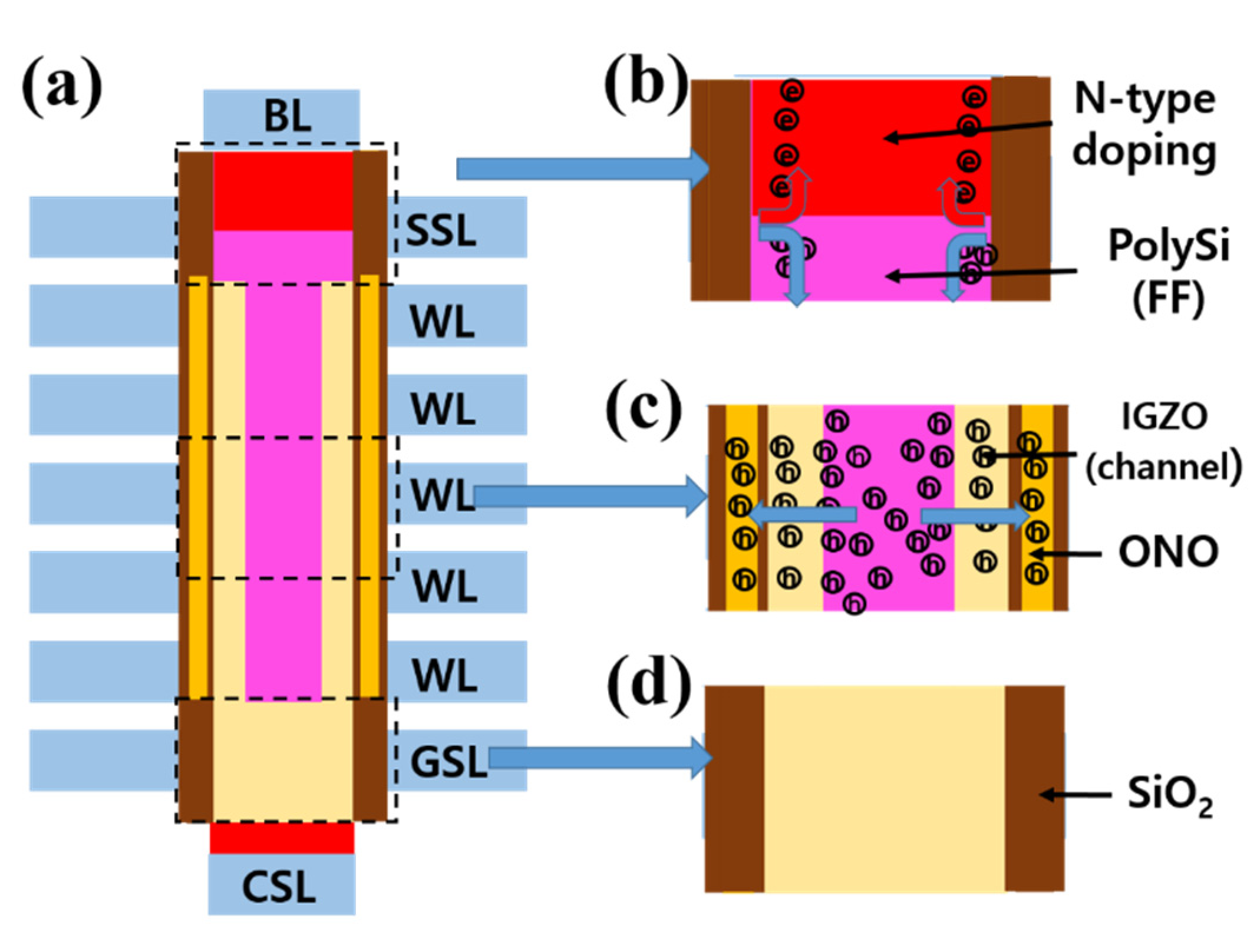
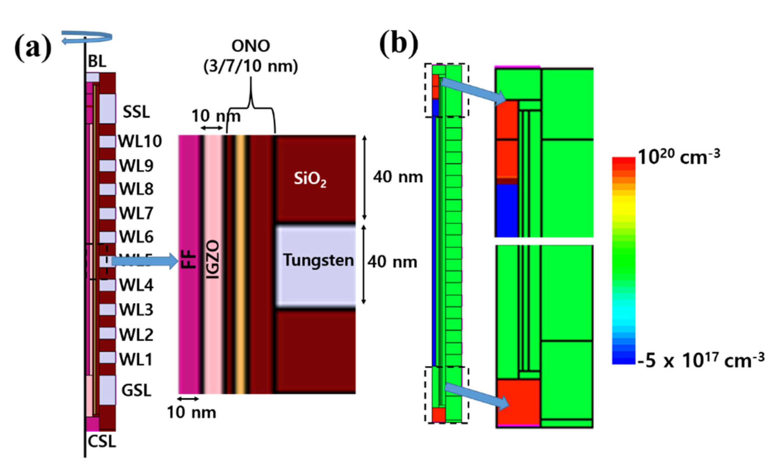
First, as shown in
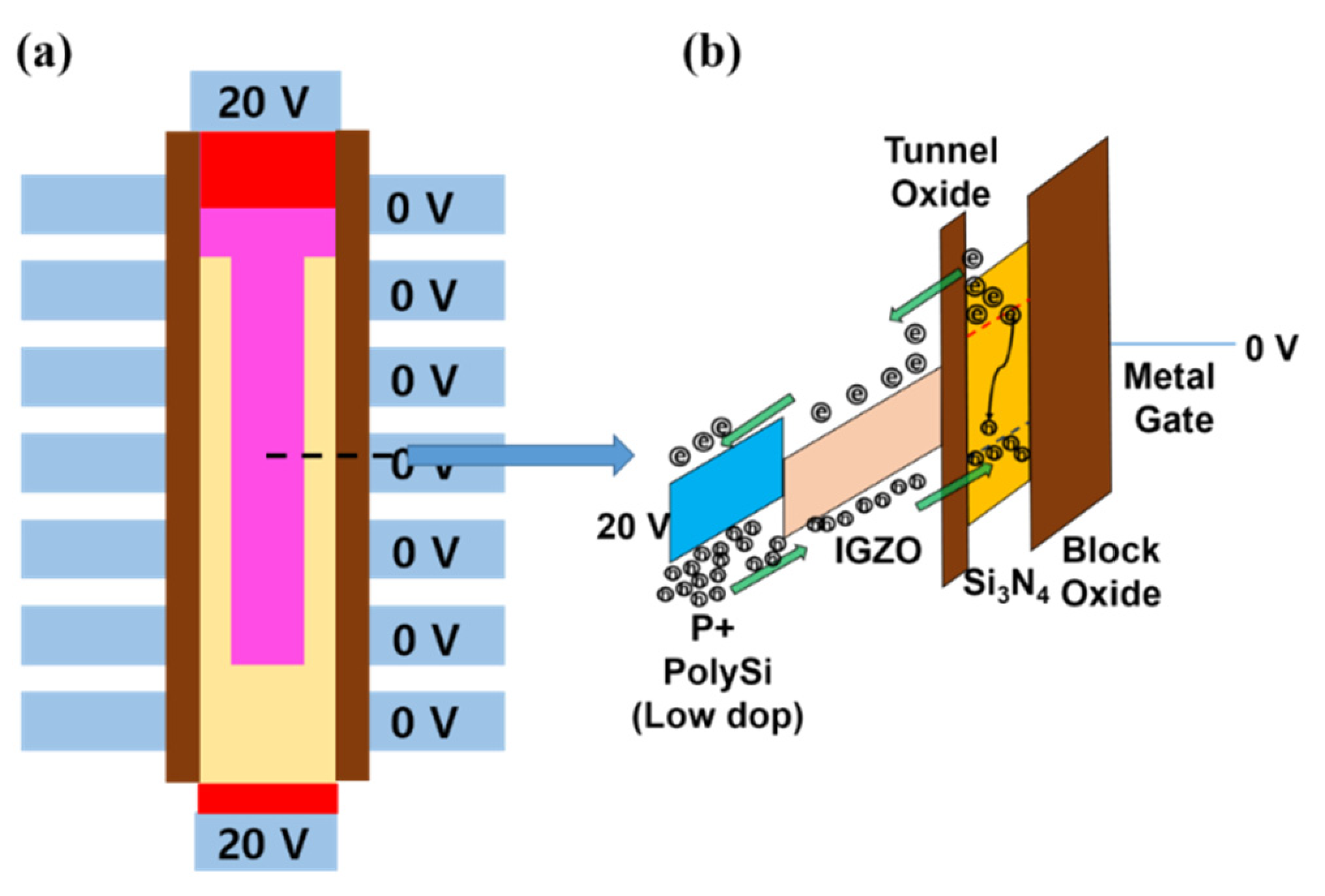
Figure 3a, the structure used had 10 word lines (WL), a string select line (SSL) at the top, and a ground select line (GSL) at the bottom. In addition, a bit line (BL) served as a drain at the top of the highest level, and a common source line (CSL) served as a source at the lowest level. Detailed information, such as descriptions and the thickness and height of the various materials, are displayed in the enlarged structure located to the right of the entire structure. Since the displayed structure shows half the entire string, the actual string diameter is 100 nm, and accordingly, the diameter of the polysilicon filler is 20 nm.
Figure 3b shows the doping states of the simulated structure. As described above, the polysilicon channel for the GIDL generation and an excessively doped region exist only in the SSL region, not the GSL region. If the same structure exists in the GSL region, holes generated by the GIDL phenomenon cannot be transferred to the IGZO channel because there is no filler, resulting in a meaningless operation. Therefore, the structure for the GIDL phenomenon should be present only in the upper SSL area connected to the filler.
Note that doping concentration dependence, high field saturation, and trap scattering mobility models were used in the device simulations. In addition, Shockley–Read–Hall, Auger, and Hurkx band-to-band recombination models were used to simulate the operation of the IGZO transistor and the V-NAND structure. The filler region in the proposed structure had a trap concentration of 5 × 10
17 cm
−3. In addition, for each material trap, the parameters listed in
Table 1 for polysilicon, IGZO, and silicon nitride were applied.
Table 2 shows the applied voltages for each operation.
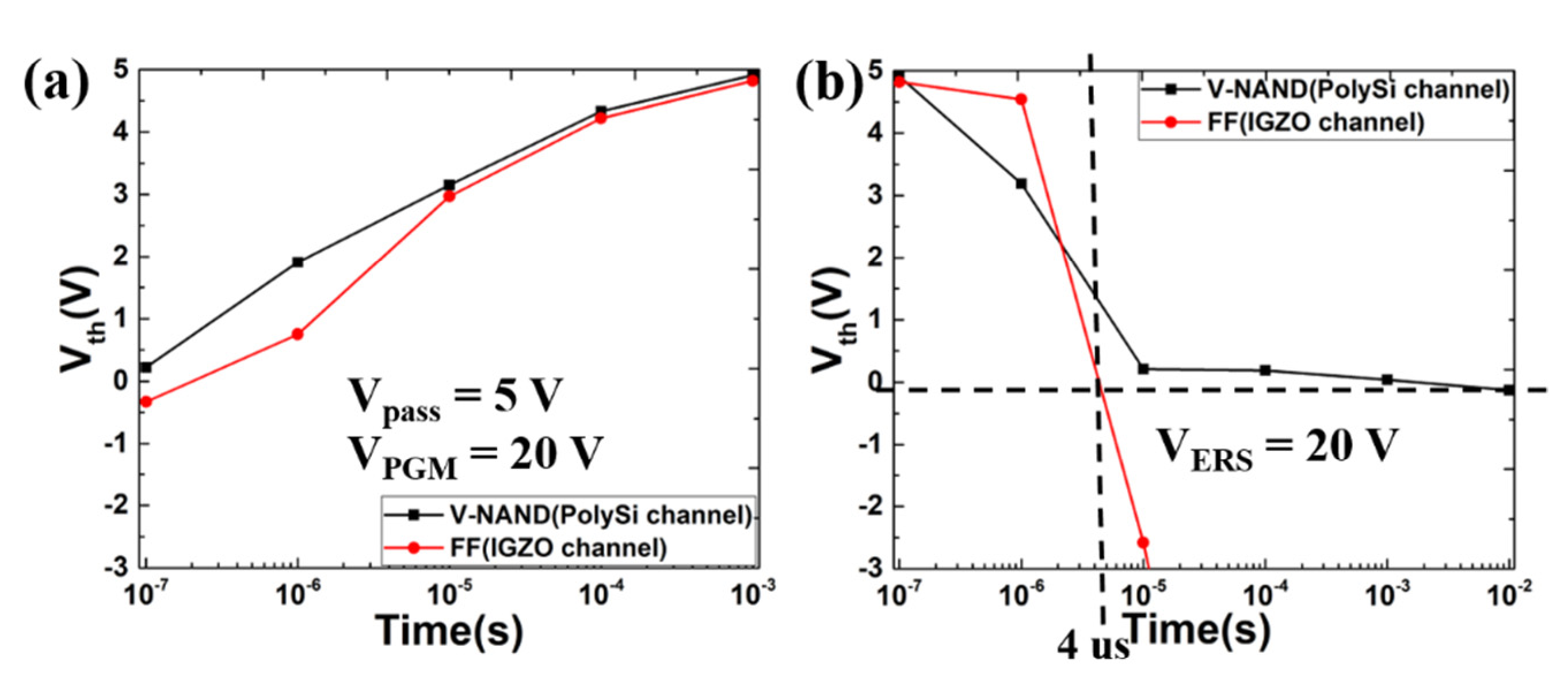
Figure 4 shows the memory operation simulation results using the V-NAND structure of a general polysilicon channel and the FF structure of the proposed IGZO channel. The proposed FF structure showed a very fast erase speed, as we expected. Specifically, the erase rate of the known erase operation of the conventional V-NAND structure was 10 ms, whereas the erase rate of the proposed FF structure was 4 μs.
These results suggest that the proposed FF structure requires very little time, so it is expected that the erase operation will consume very little power. Of course, in order to accurately calculate the power consumption in the erase operation, the high voltage circuit required to generate a high erase voltage must be considered, but the voltage used for the erase operation of the proposed structure is the same as the voltage used in the conventional V-NAND structure. Therefore, the only difference in the calculation of energy consumption is the operating time. Based on this, we expect that the proposed FF structure will consume approximately 1000 times less energy during the erase operation than the existing V-NAND structure.
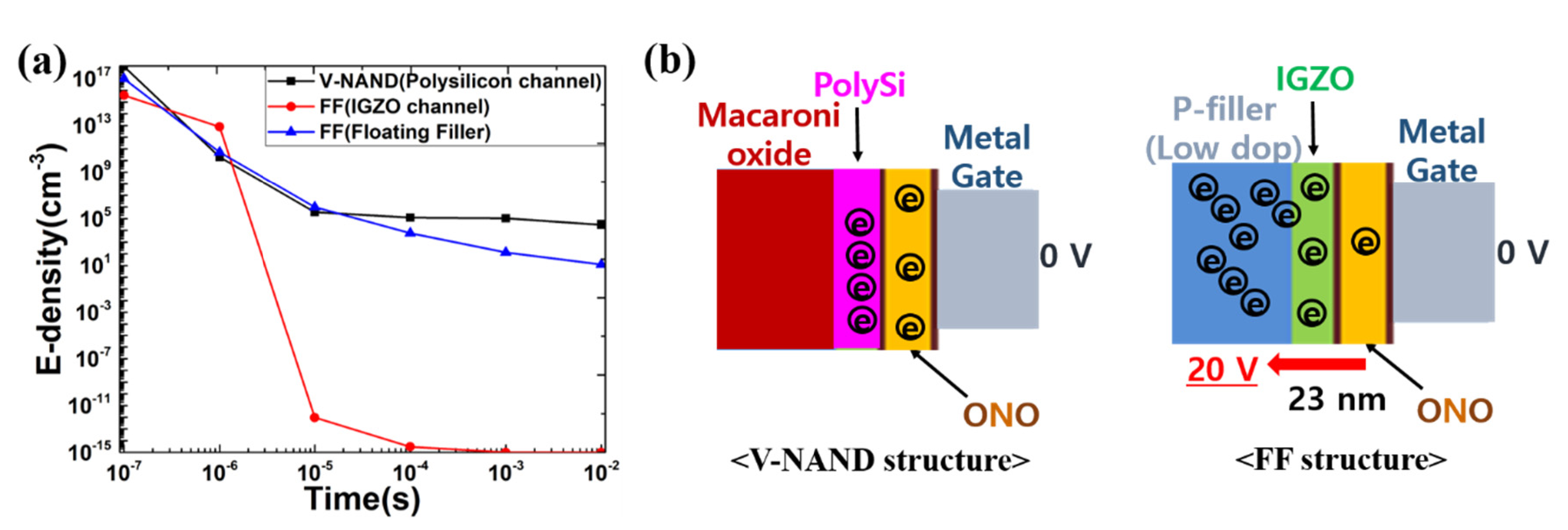
The cause of the outstanding erasing performance of the proposed FF structure is explained in
Figure 5. First, considering the change in the electron density of each channel during the erasing operation shown in
Figure 5a, in the case of the existing V-NAND structure, similar to the change in the threshold voltage, after 10 μs, electron density was almost constant at 10
5 cm
−3. On the contrary, in the case of the proposed FF structure, it can be seen that, similar to the change in the threshold voltage, electron density rapidly decreased after 1 μs and approached zero. On the contrary, it can be seen that the electron density of the FF structure adjacent to the IGZO channel maintained a relatively high value of 10
5 to 100 cm
−3 during the erasing operation. As a result of this, it can be considered that the electrons emitted from the silicon nitride layer during the erasing operation in the FF structure do not accumulate in the channel but are emitted directly to the bit line contact through the filler.
Figure 5b shows the movement of electrons during the erase operation. As mentioned above, in the existing V-NAND structure, electrons emitted from the silicon nitride layer during the erase operation enter the channel and then move in the direction of each contact because of the high voltage of the bit line (BL) or common source line (CSL). However, this movement means that many electrons emitted from silicon nitride through very thin channels have to be moved a long distance by the high voltage of distant contacts. Therefore, the electron density of the channel is always kept high during the erase operation, and electrons remain in place. By contrast, in the FF structure, the emitted electrons are immediately attracted by the high voltage of the filler and move to the filler. For this reason, the electron density of the channel can always be kept low, and the movement of electrons is very fast. Because of these advantages, the proposed FF structure does not cause congestion of electron movement and has a very fast erase speed.
Overall, we confirmed that the proposed FF structure uses the GIDL erase method but has an extremely fast erase speed similar to that of the INP and IP structures proposed in previous studies because of the presence of filler inside the channel. This indicates that the proposed structure can use the operation of existing V-NANDs while maintaining the unique characteristics of the IGZO channel, including a low leakage current and stable temperature change performance.
Next, the most important gate in the proposed structure is the GSL, which controls the current in the CSL direction during V-NAND operation to suppress the leakage current in the standby state and plays an important role in program suppression mode during multi-string operation. In particular, in the case of the SSL, which is required for stronger and more accurate operation for the same reasons, a polysilicon channel must be used to generate the GIDL phenomenon. Therefore, the structure and operating characteristics of the novel V-NAND proposed here, such as the leakage current, will be similar to those of existing V-NAND structures. However, if a polysilicon channel is used up to the GSL, it will not be possible to obtain the low leakage current characteristic of an IGZO channel because both gates are polysilicon channels. One of the two gates must contain an IGZO channel, and considering the COP structure, the IGZO channel should be used as the lower GSL gate. However, to use the IGZO channel in the GSL gate, the low threshold voltage of the IGZO channel FET needs to be overcome.
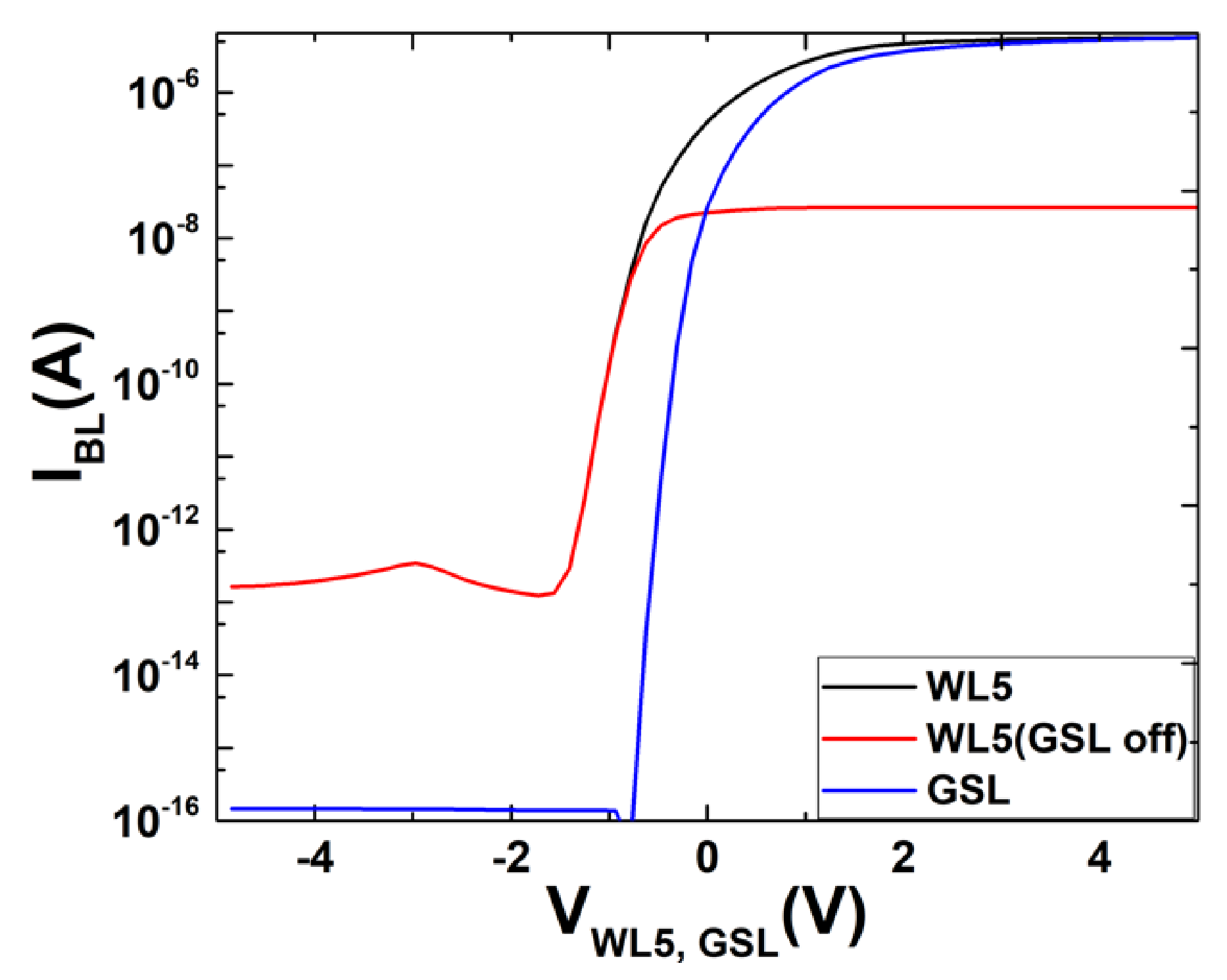
Figure 6 and
Table 3 show the results of verifying the operation characteristics of the GSL mentioned in the previous article in the proposed FF structure. this result shows a fairly high leakage current of about 10
−13 A. In addition, even if the GSL was kept in the off state, the leakage current did not decrease at all, and the high current of 10
−8 A was maintained. This result is very different from the very low leakage current (10
−15 A) of the IP structure that we previously published [
15]. Contrary to expectations, the proposed FF structure did not seem to show the low leakage current characteristic of the IGZO channel. Of course, during the normal operation (GSL on) state of WL5, the P-type filler was connected to the BL contact to which a read voltage of 1 V was applied, not the CSL contact in the GND state as in the IP structure. Therefore, the leakage current generated at this time likely flows through the polysilicon filler. We made this assumption because a leakage current of about 10
−13 A was observed in the figure, and the value of this leakage current is a typical polysilicon channel leakage current level.
However, the real problem is that the same leakage current was present even when the GSL was is in GND state and was approximately 10
−8 A when the voltage of WL5 was positive. This suggests that the GSL was not controlling the current of the entire channel. Therefore, we next examined the operation characteristics of the GSL itself, and the results are shown in blue in
Figure 6. The operating leakage current of the GSL gate with only an IGZO channel was approximately 10
−16 A. However, the threshold voltage was located in the negative region (−0.83 V). For this reason, even when the GSL gate was in the GND state, the current flowing through the IGZO channel of the GSL gate had a relatively high value of 10
−8 A. These results indicate that the high leakage current exhibited during the operation of the WL5 gate was due to the low threshold voltage of the GSL gate.
To solve this problem, a method to move the threshold voltage of the GSL gate to a positive region is required. However, changing the gate material, changing the composition of the material, or changing the material of the gate insulator to achieve this shift could increase process costs. Naturally, as the work function increases, the threshold voltage will move in the positive direction, but with a proportional increase in process cost.
Therefore, we investigated the effects of increasing the number of GSL and SSL gates or increasing the length of the gate itself to reduce the leakage current and increase gate controllability. A low threshold voltage for an IGZO channel is unavoidable because of the material properties of IGZO, which has weak N-type characteristics. Therefore, the change in the work function according to a change in the gate material or insulator material mentioned must be performed in parallel.
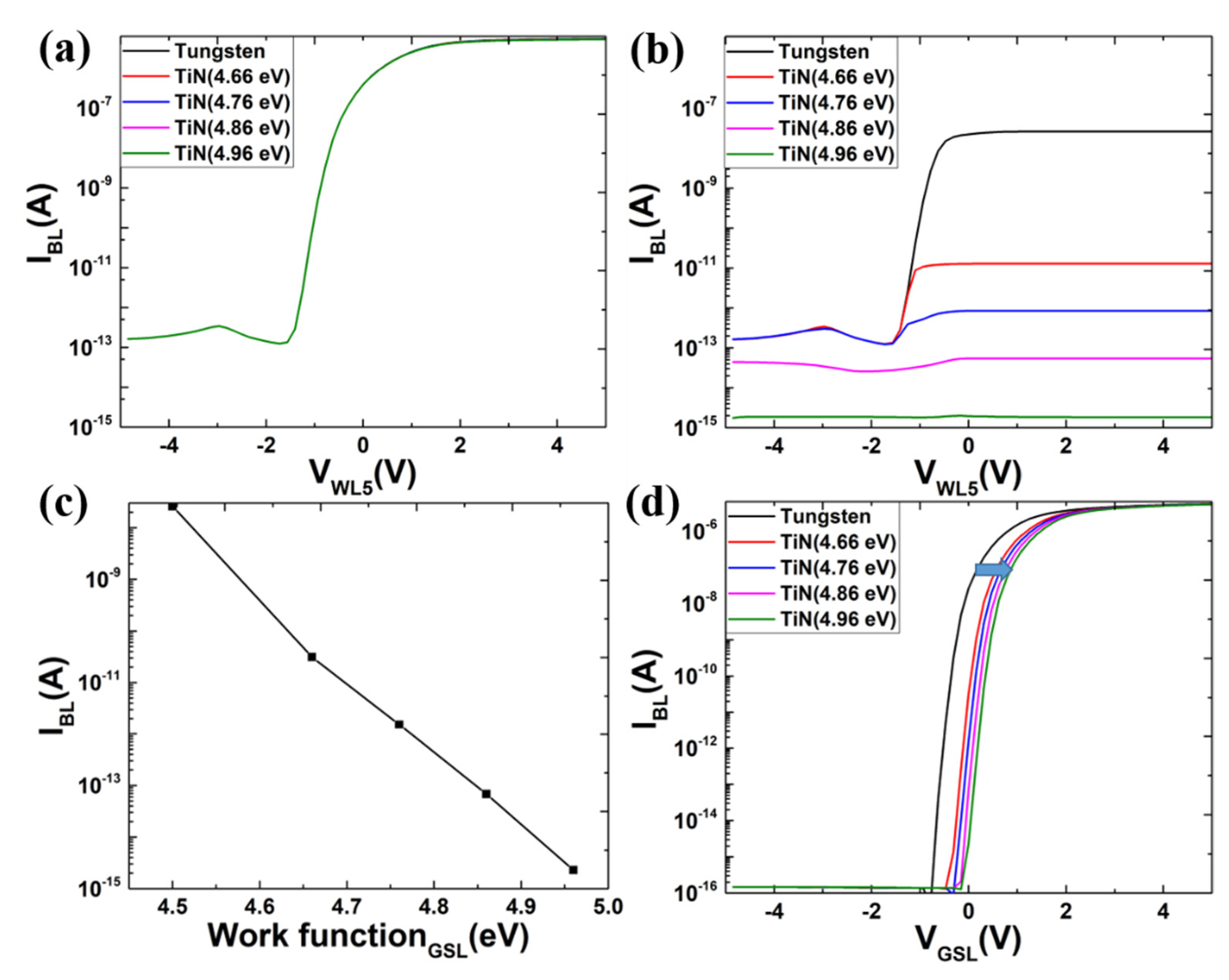
Figure 7 shows the changes in operation characteristics according to changes in the work function of GSL in the proposed structure. First, in the proposed structure, a TiN gate with a thickness of 10 nm was used as the GSL gate. The results shown in
Figure 7 are for a 100-nm-long GSL gate. A structure with a long gate can be obtained by epitaxial growth of crystal silicon, which was performed for GSL channels when using the bulk erase method prior to COP. Therefore, the above structure cannot be used in the polysilicon channel in the current COP structure, but it is possible to use this structure for an IGZO channel because of the low leakage current characteristics of IGZO channels.
Next, for the range setting of the work function change of the TiN gate, we assumed the work function would change if complex structures with various combinations of TiN or MoN were used. However, changes in the materials and structure can increase the process cost, so in this study, 5.0 eV was set as the limit [
20].
Based on the results shown in
Figure 7a, the increase in the work function of the GSL gate did not significantly affect the operating characteristics of the V-NAND, especially the on current. This led us to predict that an increase in the work function of the GSL gate would not significantly affect the operation speed of the entire string. Next, as shown in
Figure 7b, in which the GSL gate was in the off state, the leakage current rapidly decreased as the work function increased, as expected. Particularly noteworthy is that when the GSL gate work function was increased to 4.96 eV by assuming the gate material combination in the referenced paper or by other processes, the leakage current was only approximately 10
−15 A. This reflects the unique leakage current characteristics of the IGZO channel.
Figure 7c provides a summary of the change in the leakage current according to the change in the work function in
Figure 7b. It is clear from this figure that the change in the leakage current corresponding to the change in the work function was almost linear. Therefore, if the work function can be further increased by improving the gate material, the leakage current can likely be further reduced. Finally, the results shown in
Figure 7d show the I–V results of the GSL gate itself. As expected, as the work function increased, the threshold voltage moved in a positive direction by approximately 0.5 V. As a result, the amount of current flowing when the GSL gate voltage was 0 V decreased rapidly and reached 10
−15 A.
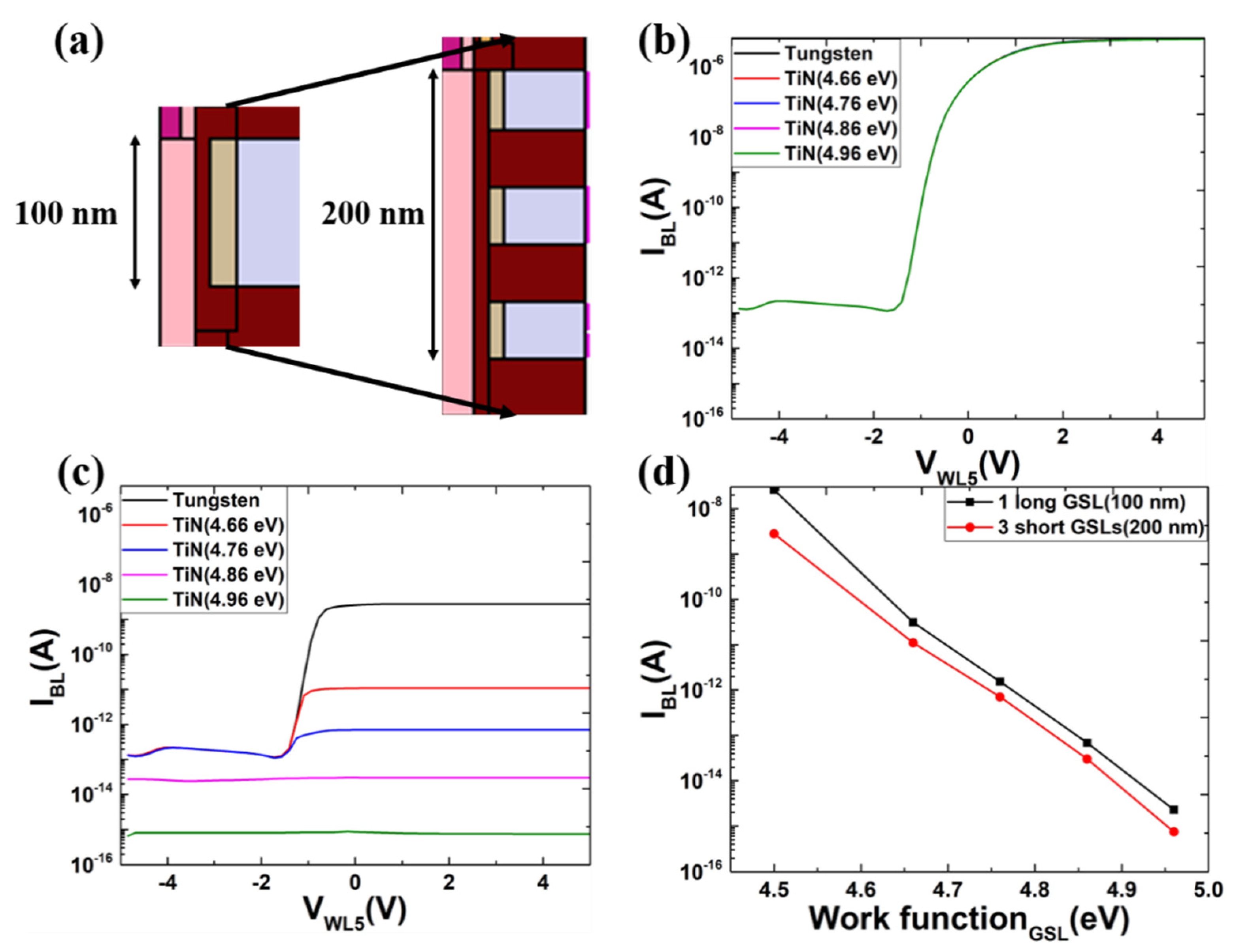
Figure 8 shows the I–V characteristics when multiple GSL gates were used. First, as shown in
Figure 8a, using a long GSL gate with a length of 100 nm and using three GSL gates with lengths of 40 nm improved the controllability of the channel. Although the length of the GSL channel doubled, the ratio of the length occupied by the entire string did not increase drastically. In fact, as shown in
Figure 8b, the current was similar to that obtained when a single GSL gate with a length of 100 nm was used. There was also no significant difference in the leakage current corresponding to the use of a single long GSL gate or multiple GSL gates. This can be attributed to the large leakage current component generated by the filler adjacent to the IGZO channel when the GSL was on. However, when the GSL gate was in the off state (
Figure 8c), the device with multiple gates showed a lower leakage current than the device with a 100-nm-long single GSL gate (
Figure 8d). In particular, when a tungsten gate (4.5 eV) was used, the leakage current decreased by 90%, but when a TiN gate (4.66–4.96 eV) was used, there was a relatively uniform reduction in the leakage current of between 65% and 68%.
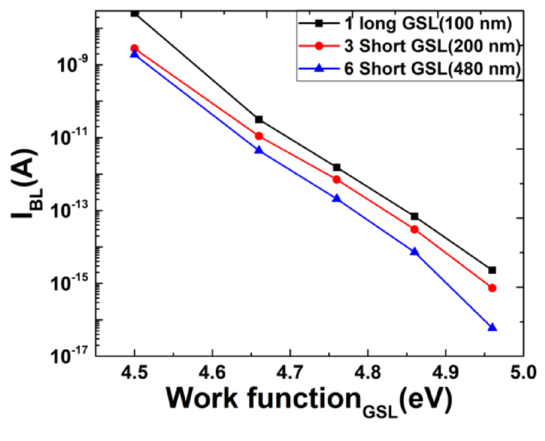
Finally,
Figure 9 shows the result of using six GSL gates for the previous leakage current change result. Notably, when the work function of the GSL gate was 4.96 eV, the leakage current could reach the theoretical expected value of 10
−17 A for IGZO materials. From these results, the proposed FF structure has the theoretical leakage current of the IGZO material because of the composition of the gate material or the combination of the constituent materials along with the change of the structure of the GSL gate, and at the same time, it shows an erasing speed that is more than 1000 times faster than the existing V-NAND structure. Of course, such a leakage current can be achieved through a change in the material composition of the IGZO channel, but in this case, there is a problem of discarding the secured mobility. Therefore, it will be important to optimize the GSL gate and particularly to establish the optimal number of GSL gates and the channel length in order to secure the maximum mobility and improve the overall operation speed, considering the high mobility and fast erase speed. When this optimization is achieved, the IGZO channel-based FF structure may be an optimal structure that shows a fast erasing speed with a reduction in power consumption due to a low leakage current.


