1. Introduction
In the memory market, 3D NAND flash memory is a mainstream technology that can achieve high bit density by increasing the mold stacking height [
1]. Recently, 3D NAND flash has been implemented with approximately 170 stacks and is expected to increase by about 300 layers [
2,
3,
4].
To continuously increase stacking layers, vertical scaling is inevitable to reduce mold staking height. However, the scaling technology has many problems which must be confronted to solve reliability issues [
5,
6,
7]. Among them, conventional gate all around (GAA) type 3D NAND structures have insufficient self-boosting efficiency, because hot carrier injection (HCI) is generated by high electric field in the channel region [
8]. Additionally, the number of cells suffering from pass disturbance increases as the string length increases [
9].
In this situation, most industries try to achieve periphery under circuit architecture to reduce the chip area [
3,
4]. This structure experienced severe leakage current characteristics during a self-boosting operation [
10,
11]. As a result, after the periphery circuit process, it is impossible to form single crystalline silicon through selective epitaxial growth (SEG) of the source line for the cell array; therefore, the channel in the ground select line (GSL) area is replaced with poly silicon type, leading to more severe program and pass disturbance. In addition, as the distance between adjacent cells decreases, high electric field generated in the spacer has a significant impact on the reliability.
To solve these issues, we proposed a gate all around with back-gate (GAAB) NAND structure, and attempted to prove excellent reliability compared to the conventional GAA structure using a TCAD simulation.
2. GAAB NAND Structure
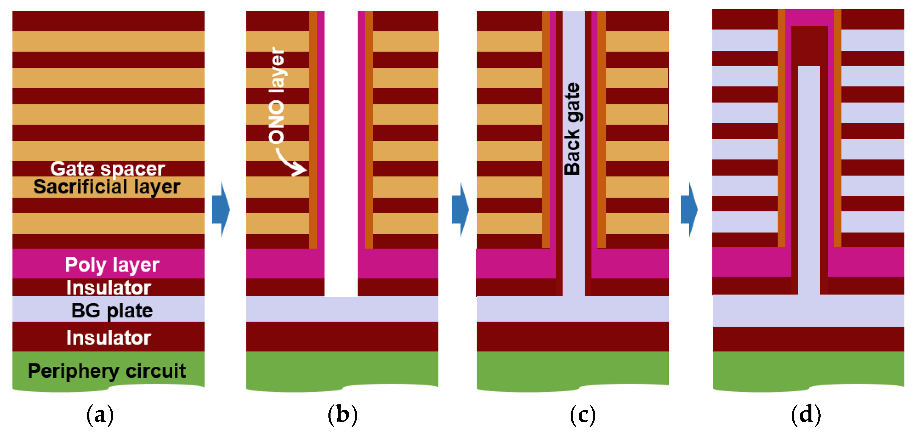
Figure 1 shows the manufacturing process flow of the GAAB structure, which can be realized by a periphery under circuit technology. In the GAA NAND type, a poly layer is formed after the formation of a periphery circuit. On the other hand, in the GAAB type, back-gate (BG) plate and insulator layer are stacked before forming the poly layer. The BG plates are formed in each block. Then, additional processes include etching the poly layer after poly-silicon channel formation and filling the BG material inside a hole after BG dielectric film deposition. These processes are the most critical steps in manufacturing the GAAB structure. Therefore, advanced etching and filling technologies are required for better feasibility. Nevertheless, the GAAB structure shows advantages in program operation.
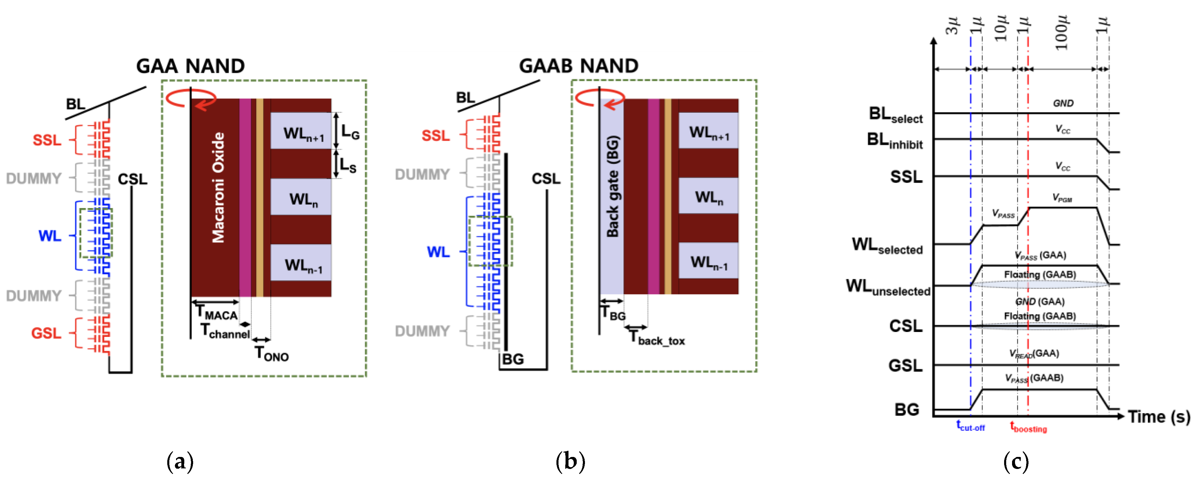
Figure 2a,b show the schematic and cross-section of the GAA and GAAB NAND structures. Compared with the conventional GAA type, GAAB shares the BG across all memory cells. Moreover, GSL transistors are not included in the GAAB structure. The operation scheme was examined in comparison with a conventional GAA structure. Both structures have 32 word-lines (WLs), and GAA uses 4 String select line (SSL)/GSL transistors while GAAB only uses SSL. The design parameters of the gate length, space length, and O/N/O thickness are 25 nm, 20 nm, and 4/6/6 nm, respectively. The macaroni oxide thickness (T
MACA) in the GAA structure is 40 nm, and both the back gate oxide thickness (T
back_tox) and back-gate thickness (T
BG) are 20 nm in GAAB. The channel thickness is 10 nm for both structures. Lastly, the selected word-line is WL16, which is the center of the string.
In the TCAD simulation-based study, we used the recombination model using the doping dependence of the SRH (Shockley–Read–Hall) lifetime model and band-to-band model. In addition, all simulation results are performed by cylindrical computation based on the cross-sections structure of
Figure 2a,b.
3. Self-Boosting Scheme of GAAB NAND
Figure 2c shows the program operation in selected bit line (BL) and inhibited BL. In the program operation, NAND flash array is controlled by each BL and SSL bias condition [
12]. Therefore, channel potential of the inhibited BL must be increased by a self-boosting scheme to prevent program disturbance. Alternatively, the channel potential of the selected BL must be grounded to maximize the electric field between WL and channel. In the case of a conventional self-boosting scheme, SSL and GSL channel regions must make the cut-off state by applying
VCC bias, which leads to a floating state in inhibited channel potential at t
cut-off. After this,
VPASS and
VPGM bias to the unselected and selected WLs can increase the floating state channel potential at t
boosting.
Compared with the conventional program scheme, program operation of the GAAB NAND structure uses BG bias to increase channel potential. Therefore, unselected WLs are in the floating state, and the pass voltage (VPASS) is applied to the back gate instead. Common source line (CSL) is also in a floating state as the unselected WL. In this scheme, we observed tboosting when the selected WL is applied in the VPGM.
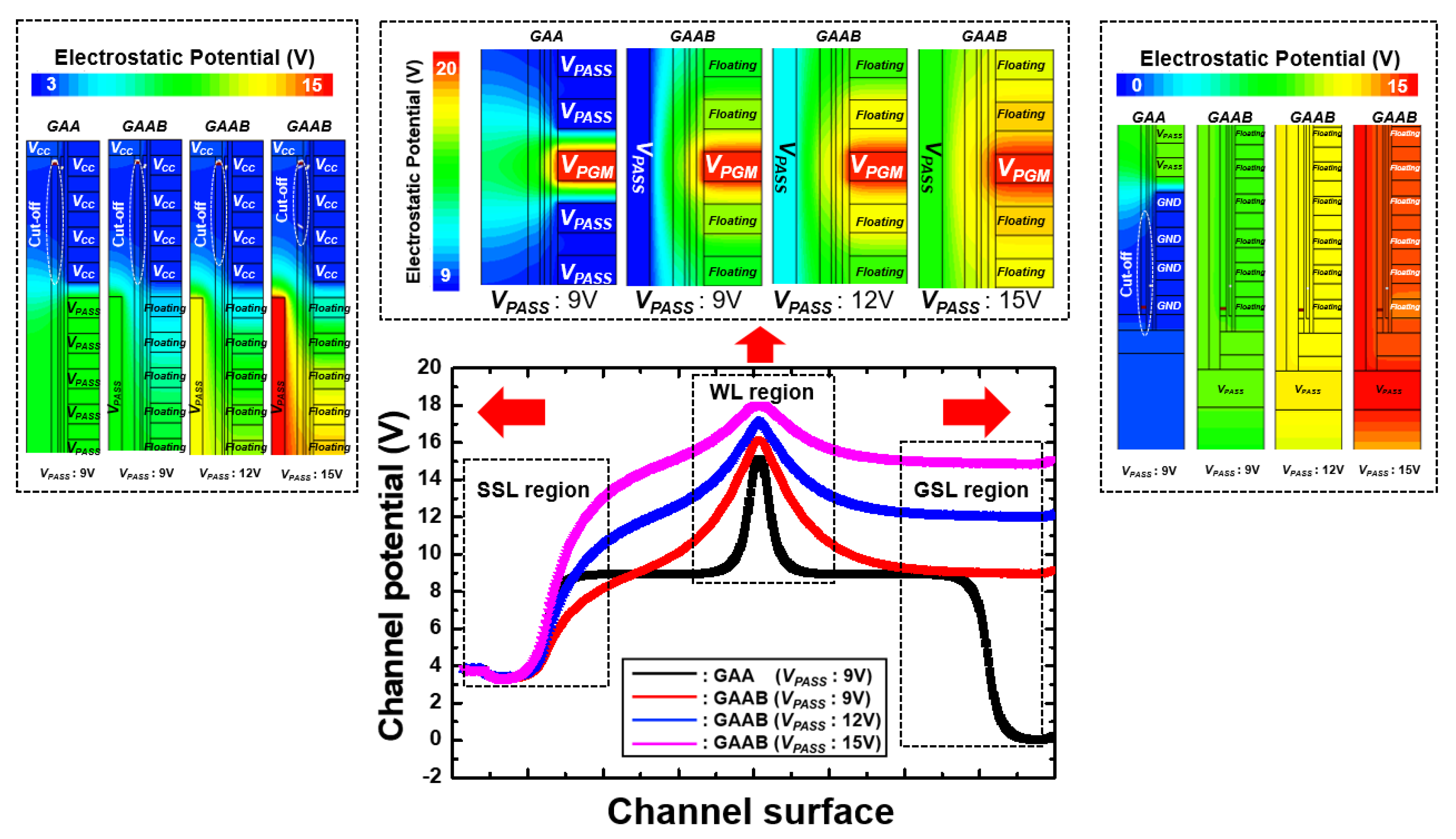
Figure 3 shows the channel potential of GAA and GAAB NAND structures in the inhibited BL and electrostatic potential at each region at t
boosting. The channel potential characteristics of GAA NAND shows the general self-boosting effect [
13]. Therefore, the potential difference between the selected WL and unselected WL is abruptly increased.
However, the GAAB structure shows a gradual profile of channel potential since the unselected WLs are in a floating state. Additionally, the channel potential can be easily increased by increasing the VPASS without considering the pass disturbance. Therefore, the VPASS of the unselected WL can be completely replaced by applying VPASS to the back gate in the GAAB NAND. Furthermore, we also confirmed that GAAB NAND strings achieve self-boosting behavior without GSL transistors. Although both GAA and GAAB have the same cut-off operation in the SSL region, in the case of the GSL region, GAAB does not need GSL—unlike GAA—because GSL is not required due to back gate bias under the poly layer. Since the 3D NAND flash technologies use the poly-silicon channel of SSL and GSL transistors, the leakage characteristics must be carefully considered. However, we confirmed that the GAAB structure can achieve program operation without a GSL transistor. It will be an advantage for reducing the burden on the manufacturing process and circuit operation.
4. Reliability Characteristics
In this chapter, we investigated reliability characteristics of the GAAB NAND structure compared with GAA. We focused on program disturbance and pass disturbance. The program disturbance occurs in the inhibited BL.
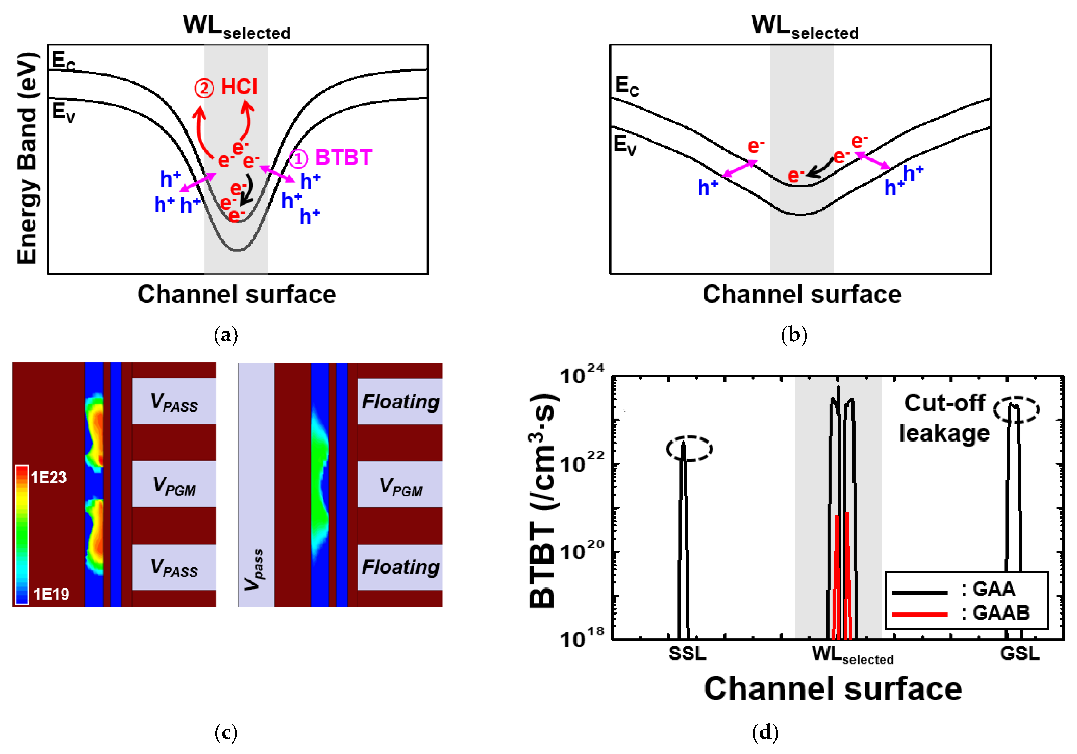
Figure 4a shows the energy band diagram of the GAA structure. Since the energy band near the selected WL is steep, band-to-band tunneling (BTBT) generation may occur. The generated electrons are likely to cause HCI due to a high electric field.
Alternatively,
Figure 4b shows that the GAAB band diagram is a very gradual slope, which is expected to have significantly less BTBT generation compared with the GAA structure. As a result,
Figure 4c,d show a simulated result of BTBT generation. The GAAB structure has significantly lower BTBT generation than that of the GAA structure. In addition,
Figure 4e shows BTBT generation occurring in the inhibited BL channel. In the GAA structure, BTBT generation is also high in the SSL and GSL transistor areas, which is caused by the potential difference between unselected WL and cut-off region in SSL and GSL as shown in
Figure 3b. On the other hand, BTBT generation hardly occurs on SSL and GSL in the GAAB structure due to the gradual channel potential slope with the cut-off region of the SSL channel area.
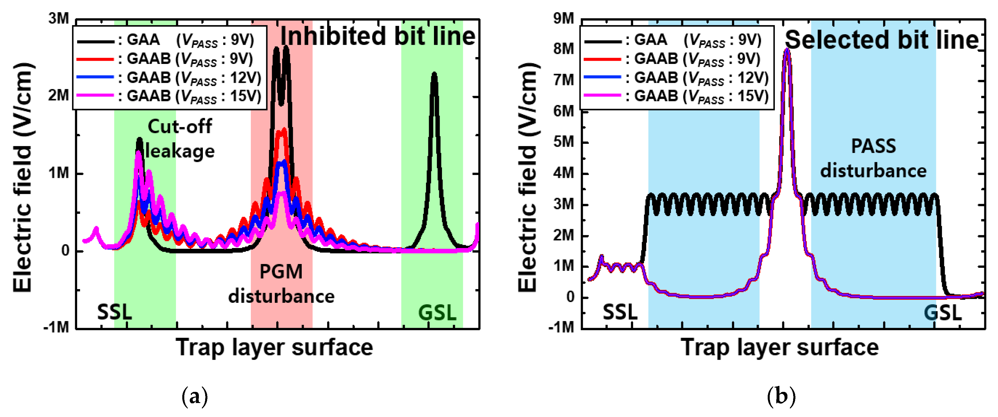
Figure 5a shows the electric field in the nitride trap layer. Even if
VPASS increases, the electric field in the selected WL, SSL, and GSL region is lower in the GAAB structure than in the GAA structure. The high electric field in the trap layer can also affect the retention characteristic of trapped charge. Therefore, we confirmed that the GAAB structure has significant immunity to program disturbance.
Figure 6 shows the electric field contour in inhibited BL. During program operation, the potential difference between selected WL (VPGM = 20 V) and unselected WLs (V
PASS = 9 V) is critical for the break down issue, as shown in
Figure 6a. However, the GAAB structure provides more immunity to breakdown because the floating state of unselected WL can be maintained at a relatively lower electric field than the GAA structure due to the gradual potential distribution between WLs, as shown in
Figure 6b.
Considering all the advantages investigated above, the GAAB NAND has a number of advantages for high stacking and vertical shrinkage structures.
5. Conclusions
A gate all around with back-gate (GAAB) structure was proposed for 3D NAND flash memory technology. Excellent characteristics of the proposed structure were demonstrated by a self-boosting scheme using back gate bias. It provides a highly gradual channel profile, which leads to high immunity of program disturbance, pass disturbance and overcoming of the field breakdown between WLs. These advantages of the GAAB structure can lead to a significant increase in the number of cells by scaling down and better reliability characteristics.
Author Contributions
Methodology, paper writing, investigation, conceptualization, Validation, writing, investigation, J.-M.S. Review, B.-S.K. and I.-H.N. Funding acquisition, supervision, editing, Y.-H.S. All authors have read and agreed to the published version of the manuscript.
Funding
This research was supported by PeDiSem Co., Ltd.
Conflicts of Interest
The authors declare no conflict of interest.
References
- Park, K.-T.; Nam, S.; Kim, D.; Kwak, P.; Lee, D.; Choi, Y.-H.; Choi, M.-H.; Kwak, D.-H.; Kim, D.-H.; Kim, M.-S.; et al. Three-Dimensional 128 Gb MLC Vertical nand Flash Memory with 24-WL Stacked Layers and 50 MB/s High-Speed Programming. IEEE J. Solid State Circuits 2015, 50, 204–213. [Google Scholar] [CrossRef]
- Kang, D.; Kim, M.; Jeon, S.C.; Jung, W.; Park, J.; Choo, G.; Shim, D.K.; Kavala, A.; Kim, S.B.; Kang, K.M.; et al. 13.4 A 512Gb 3-bit/Cell 3D 6th-Generation V-NAND Flash Memory with 82MB/s Write Throughput and 1.2Gb/s Interface. In Proceedings of the 2019 IEEE International Solid- State Circuits Conference—(ISSCC), San Francisco, CA, USA, 17–21 February 2019; pp. 216–218. [Google Scholar] [CrossRef]
- Huh, H.; Cho, W.; Lee, J.; Noh, Y.; Park, Y.; Ok, S.; Kim, J.; Cho, K.; Lee, H.; Kim, G.; et al. 13.2 A 1Tb 4b/Cell 96-Stacked-WL 3D NAND Flash Memory with 30MB/s Program Throughput Using Peripheral Circuit Under Memory Cell Array Technique. In Proceedings of the 2020 IEEE International Solid- State Circuits Conference—(ISSCC), San Francisco, CA, USA, 16–20 February 2020; pp. 220–221. [Google Scholar]
- Siau, C.; Kim, K.H.; Lee, S.; Isobe, K.; Shibata, N.; Verma, K.; Ariki, T.; Li, J.; Yuh, K.; Amarnath, A.; et al. 13.5 A 512Gb 3-bit/Cell 3D Flash Memory on 128-Wordline-Layer with 132MB/s Write Performance Featuring Circuit-Under-Array Technology. In Proceedings of the 2019 IEEE International Solid- State Circuits Conference—(ISSCC), San Francisco, CA, USA, 17–21 February 2019; pp. 218–220. [Google Scholar] [CrossRef]
- Alsmeier, J.; Higashitani, M.; Paak, S.S.; Sivaram, S. Past and Future of 3D Flash. In Proceedings of the 2020 IEEE International Electron Devices Meeting (IEDM), San Francisco, CA, USA, 12–18 December 2020; pp. 103–106. [Google Scholar]
- Compagnoni, C.M.; Spinelli, A.S. Reliability of NAND Flash Arrays: A Review of What the 2-D–to–3-D Transition Meant. IEEE Trans. Electron. Devices 2019, 66, 4504–4516. [Google Scholar] [CrossRef]
- Goda, A. 3-D NAND Technology Achievements and Future Scaling Perspectives. IEEE Trans. Electron. Devices 2020, 67, 1373–1381. [Google Scholar] [CrossRef]
- Park, I.H.; Hahn, W.-G.; Song, K.-W.; Choi, K.H.; Choi, H.-K.; Lee, S.B.; Lee, C.-S.; Song, J.H.; Han, J.M.; Kyoung, K.H.; et al. A new GIDL phenomenon by field effect of neighboring cell transistors and its control solutions in sub-30 nm NAND flash devices. In Proceedings of the 2012 Symposium on VLSI Technology (VLSIT), Honolulu, HI, USA, 12–14 June 2012; pp. 23–24. [Google Scholar]
- Zhang, Y.; Jin, L.; Zou, X.; Liu, H.; Zhang, A.; Huo, Z. A Novel Program Scheme for Program Disturbance Optimization in 3-D NAND Flash Memory. IEEE Electron. Device Lett. 2018, 39, 959–962. [Google Scholar] [CrossRef]
- Zhang, Y.; Jin, L.; Jiang, D.; Zou, X.; Zhao, Z.; Gao, J.; Zeng, M.; Zhou, W.; Tang, Z.; Huo, Z. Leakage characterization of top select transistor for program disturbance optimization in 3D NAND flash. Solid State Electron. 2018, 141, 18–22. [Google Scholar] [CrossRef]
- Resnati, D.; Goda, A.; Nicosia, G.; Miccoli, C.; Spinelli, A.; Compagnoni, C.M. Temperature Effects in NAND Flash Memories: A Comparison Between 2-D and 3-D Arrays. IEEE Electron Device Lett. 2017, 38, 461–464. [Google Scholar] [CrossRef]
- Yoo, H.; Choi, E.; Oh, J.; Park, K.; Jung, S.; Kim, S.; Shim, K.; Joo, H.; Jeon, K.; Seo, M.; et al. Modeling and optimization of the chip level program disturbance of 3D NAND Flash memory. In Proceedings of the 2013 5th IEEE International Memory Workshop 2013, Monterey, CA, USA, 26–29 May 2013; pp. 147–150. [Google Scholar] [CrossRef]
- Kang, M.; Kim, Y. Natural Local Self-Boosting Effect in 3D NAND Flash Memory. IEEE Electron. Device Lett. 2017, 38, 1236–1239. [Google Scholar] [CrossRef]
| Publisher’s Note: MDPI stays neutral with regard to jurisdictional claims in published maps and institutional affiliations. |
© 2021 by the authors. Licensee MDPI, Basel, Switzerland. This article is an open access article distributed under the terms and conditions of the Creative Commons Attribution (CC BY) license (https://creativecommons.org/licenses/by/4.0/).


