Abstract
This paper presents a comprehensive review based on the features and drawbacks of the quasi-switched boost inverter (qSBI) topologies. The qSBI derived configurations are well suitable for low power applications due to their reduced number of components. This work focuses on the topological review of qSBI derived topologies and serves as a reference for further derivation and research on the selection of suitable topology for the specific renewable energy applications, particularly based on the photovoltaic (PV) converters.
1. Introduction
Renewable energy source-based power generation plays an important role in satisfying global energy demand. The renewable energy sources (RES), like wind and photovoltaics, have changed the current scenario of the global energy structure. The selection of suitable inverter topology is an important factor to be considered in the renewable energy system design to improve the efficiency of the system and to maximize the energy extraction. Two basic topologies for DC–AC power conversion are voltage source inverter (VSI) and current source inverter (CSI). The VSI has the limitations of the output voltage which cannot exceed source voltage and the output voltage of CSI cannot be lower than the input voltage. Additionally, the power switches of the same leg cannot be turned on simultaneously in VSI and cannot be turned off at the same time in CSI. The impedance source (Z-source) converter introduced in 2002 outperforms the traditional VSI with buck-boost abilities in a single-stage power conversion and overcomes the shoot-through problems [1].
Z-source converters have emerged as one of the most promising and competitive converter topologies suitable for applications based on RES or alternative energy sources due to their capability of the extended input voltage regulation range. Z-source inverters (ZSI) was first proposed for the DC–AC conversion applications and then widened to DC–DC, AC–DC, AC–AC conversion applications [2,3,4,5,6,7,8,9]. ZSI consists of an LC pair in X-configuration network and transfers the temporary energy within the network during the shoot-through and non-shoot-through stages. The outstanding features of ZSI has attracted a lot of research and resulted in the development of several derived topologies like quasi-Z-source inverter (qZSI), magnetically coupled impedance network, embedded Z-source, Trans-Z-source, Γ-Z-source derived network, LCCT Z-source and qZSI, Y-source impedance network derived topologies, L–Z-source converter, Sigma Z-source converter, Δ-source impedance network derived topologies, A-source impedance network derived topologies, coupled-inductor, switched-inductor derived Z-source and quasi-Z-source topologies, and extended boost topologies. The extended boost ZSI and qZSI topologies are capable of producing infinite boost.
The qZSI topology derived from the ZSI inherits all the merits such as single-stage power conversion along with the benefits of reduced capacitor voltage stress with improved input current profile and reliability [10]. These unique merits of the qZSI topology have attracted a wide range of research for different applications [11,12,13,14,15] and resulted in several derived topologies of qZSI over the years.
The literature [16,17,18,19,20] presents a good overview of the various impedance source converter topologies. However, the practical implementation of extended boost topologies is not popular due to their use of large number of components and additional power losses [21,22,23,24]. Only few attempts of industrial design can be found [25,26].
In [27], two switched boost inverter (SBI) topologies are presented as simpler alternative solution to the ZSI with only half of the passive components. Figure 1a,b shows the SBI topologies derived from the inverse Watkins–Johnson topology and are well suited for low power applications. The SBI topology comprises a switched impedance network with a capacitor, inductor and a pair of diodes with an active switch. In SBI Type 1, the capacitor is connected to the negative DC bus, and in SBI Type 2 the capacitor is connected to the positive side of the DC bus. The operation of the SBI topology is similar to the ZSI in the shoot-through state and can replace the ZSI in low power application due to the presence of one less LC pair. The drawbacks of the SBI are high voltage stress on the capacitor, lower boot factor than impedance source converter, and discontinuous input current. In [28], two Trans-SBI topologies are presented with a two-winding transformer in place of the inductor in the traditional SBI. In Trans-SBI Type 1, the capacitor is connected to the negative side of the H-bridge inverter. In Trans-SBI Type 2, the capacitor is connected to the positive side of the H-bridge inverter. Figure 1c,d presents the Trans-switched boost inverter topologies Type 1 and Type 2.
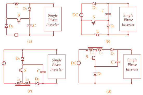
Figure 1.
(a) Switched boost inverter (SBI) topologies Type 1; (b) Switched boost inverter (SBI) topologies Type 2; (c) Trans switched-boost inverter Topologies Type 1; (d) Trans switched-boost inverter topologies Type 2.
In [29], switched inductor derived SBIs (SL-SBI) are presented with high step-up DC-link voltage. They are derived from the SBI by adding one inductor and three diodes. The SL-SBI and Trans-SBI have better efficiency and fewer components compared to the SL-ZSI and Trans-ZSI topologies. Several topologies can be derived from the basic SLBI by changing the place of the input DC source. By placing the input source in the place of DC source 1, two SLBI topologies can be derived as SLBI Type 1 and Type 2. In SLBI Type 1, the capacitor is connected to the negative side of the H-bridge inverter. In SLBI Type 2, the capacitor is connected to the positive side of the H-bridge inverter. Several topologies can be derived from the basic SLBI by changing the place of the input DC source. The continuous input current SLBI is derived by placing the input source in the place of the DC Source 4. The discontinuous input current SLBI can be derived by placing the input DC voltage source in the place of the DC Source 2. In discontinuous input current SLBI, the DC source is in series connection with the diode, resulting in discontinuous input current. A ripple input current SLBI can be obtained by placing the input source in the place of DC Source 3. In this configuration, the source current flows to the SL cell, resulting in input current ripples. Figure 2a,b presents the switched-inductor boost inverter (SLBI) Type 1 and Type 2 configurations.
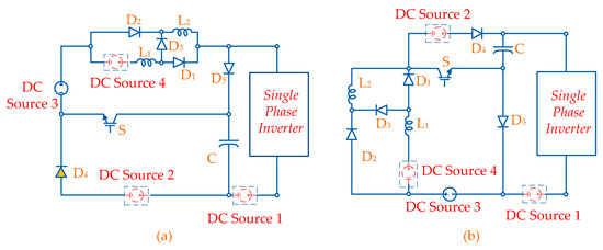
Figure 2.
Switched-inductor boost inverter (a) Type 1; (b) Type 2.
2. Overview of Original Quasi-Switched Boost Topologies (qSBI)
In [30], a class of quasi-switched boost inverter (qSBI) topologies is presented as an alternative solution to the quasi-Z-source inverter. An overview comparison of qZSI and qSBI is presented in [31]. The qSBI topology originally derived from the SBI topology utilizes the same number of components and offers reduced voltage stress on the capacitor, increased boost factor with improved input current profile. Figure 3a,b shows the embedded qSBI Type 1 and Type 2 configurations. In E-qSBI type 1, the input ground is not shared with the inverter bridge ground. In E-qSBI type 2, the input ground and inverter bridge share the same ground.
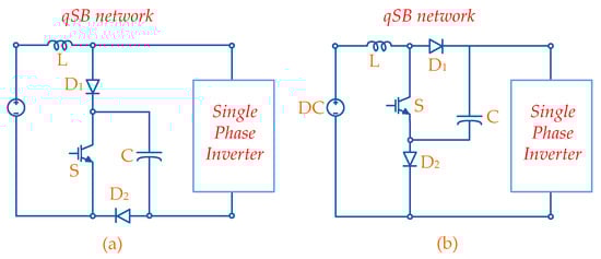
Figure 3.
Embedded quasi-switched boost inverter (SBI) topologies. (a) Type 1; (b) Type 2.
Several modulation techniques were proposed in [32,33,34,35,36,37] for qSBI to improve the voltage gain. In [30], the simple boost control (SBC) method was presented for the qSBI topologies. Figure 4 presents the PWM SBC strategy for the qSBI. In the SBC method, the control signals are generated by comparing a constant voltage to the triangular waveform. The control signal for Switch S is generated by comparing a constant voltage signal with another double frequency triangular waveform of half the amplitude and then inserted into the control signal of switches S1-S4 as shoot-through (ST) signal. In the SBC method, the maximum duty ratio of ST state is limited by (1-M) and reduced modulation index resulting in lower DC–AC conversion gain and higher THD. To overcome this drawback, an improved PWM control method with a higher modulation index was presented in [32]. The control signals for the switches S1-S4 are generated by comparing two reference voltages with a high frequency triangular waveform T1. The control signal for the Switch S is generated by comparing a constant voltage signal with a high frequency sawtooth waveform. The ST signal is generated by comparing the constant voltage signal with another triangular waveform T2 and then inserted into the H-bridge switch control signals using logic gates OR. The improved PWM technique offers high boost conversion, reduced voltage stress on the passive components, improved efficiency and reduced ST current. This PWM technique has the drawback of the high peak value of LF capacitor voltage and inductor current. In [33], the maximum boost PWM control method is presented for single-phase qSBI topology with improved modulation index. In MBC method, the control signals for H-bridge switches are generated by comparing two sinusoidal waveforms with amplitude value M to a triangular waveform. The control signal of Switch S is generated by comparing a double line frequency sinusoidal waveform to a triangular waveform of double frequency with half of the amplitude. This control signal is inserted into the H-bridge switch control signal as ST states. In this method, a variable ST time intervals are generated by inserting low frequency voltage into the constant voltage signal.
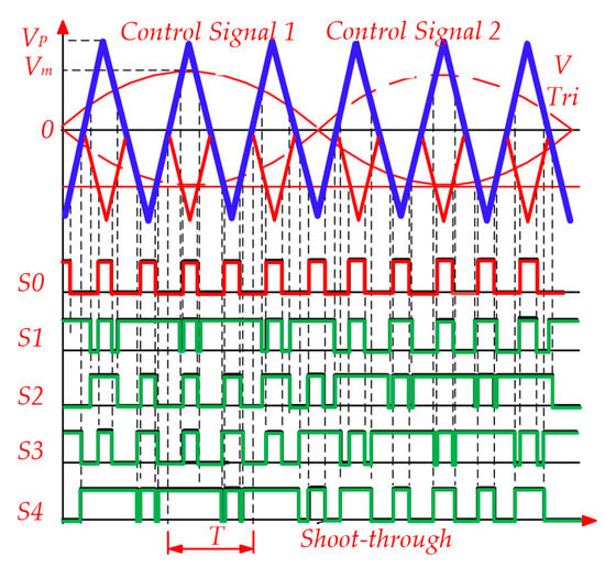
Figure 4.
PWM simple boost control strategy for the qSBI topology.
A family of PWM strategies was presented for the qSBI topologies in [34] with high reliability and reduced voltage stress on the semiconductor devices. The presented PWM techniques have reduced HF inductor current ripples. In PWM2 method, the ST signals for the H-bridge switches are generated by comparing two fixed signals with a triangular waveform of twice the frequency. The control signal for Switch S is generated by comparing a constant voltage signal with another triangular waveform. In PWM3 method, the control signal for switch S is generated by comparing two constant voltages with triangular waveform of three times frequency and 2/3 peak-to-peak value. The ST signal is inserted into the control signal of Switch S using the logic gate XOR. This PWM technique can be extended to n times by varying the triangular waveform frequency and peak-to-peak values. In the presented PWM technique, the high frequency inductor current ripple is reduced to n times. The major drawbacks of the presented techniques are complex PWM generation and higher switching losses. In [35], space vector modulation (SVM) strategy was presented for three-phase qSBI topology with high modulation index, reduced voltage stress on the components and inductor current ripple.
Figure 5 presents the four DC-Link qSBI topologies in positive and negative buses. The four DC-Link qSBI topologies have the same number of components and identical characteristics. In DC-Link qSBI negative bus type 1 and 2, the input source is inserted between the SB cell with the negative terminal of the DC bus where the input ground is shared with the bridge inverter ground. In DC-Link qSBI positive bus type 1 and 2, the input source is inserted between the SB cell with the positive terminal of the DC bus where the input ground is not shared with the bridge inverter ground. The DC-Link qSBI topology introduced alongside the E-qSBI is less favored mainly because of their low voltage gain. In [36], a modified PWM control strategy based on the maximum constant boost control (MCBC) with third harmonic injection is presented for the DC-Link qSBI. The presented control strategy improves the power conversion efficiency with enhanced voltage gain and reduced the conduction losses. A three-phase DC-Link qSBI topology is presented in [37] with improved PWM strategy by maintaining the duty cycle of the active switch as constant and the ST duty cycle as control variable. In improved PWM strategy, the switch S is triggered outside the ST time interval by comparing a reference signal with the triangular waveform. The ST states are generated by comparing another reference signal with carrier frequency triangular waveform. The DC-Link qSBI with improved PWM control strategy is suitable for applications where a minimal boost is required. Compared to the qZSI topology, the E-qSBI and DC-qSBI have better efficiency with less passive components.
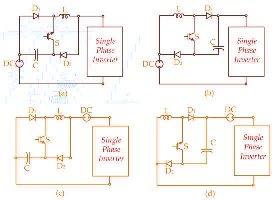
Figure 5.
DC-Link quasi-switched boost topologies (a) For negative bus type 1; (b) For negative bus type 2; (c) For positive bus type 1; (d) For positive bus type 2.
3. QSB Derived Topologies
For maximum energy extraction, RES requires high-voltage gain inverters. To improve the moderate voltage gain of the qSBI topology several derived topologies like switched-inductor qSBI, cascaded switched-inductor qSBI, half-bridge qSBI, four-switch qSBI, capacitor-switched qSBI, high-gain qSBI, and derived configurations like voltage multiplier cell qSBI (VMC-qSBI), cascaded qSBI configurations, interleaved qSBI, qSB T-Type inverter topologies were developed over the years. Figure 6 presents the various derived topologies and configurations of qSBI.
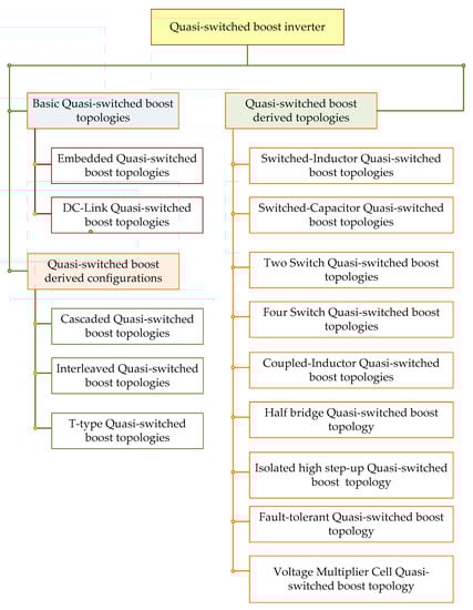
Figure 6.
Quasi-switched boost derived topologies and configurations.
A switched-inductor derived qSBI topology (SL-qSBI) is presented in [38], with a switched-inductor cell added to the qSBI topology to increase the DC voltage gain. The SL cell is one of the most extensively used techniques to improve the voltage gain. Compared to the SL-ZSI topologies, the SL-qSBI has reduced losses due to reduction in the passive components size and offers high boost inversion ability. The SL-qSBI has the drawback of higher input current ripple compared to the traditional qSBI. In [39], an improved switched inductor qSBI topology (cSL-qSBI) is proposed with a modified switched inductor structure. The SL-qSBI and cSL-qSBI topologies are shown in Figure 7a,b. The cSL-qSBI has the benefit of reduced input current ripples compared to the SL-qSBI topology. The cSL-qSBI is derived from the SL-qSBI by connecting one inductor of the switched-inductor cell in series with the input source and has the same number of components as SL-qSBI. The presented topology features a simpler structure with high voltage DC gain and enhanced power density. The cSL-qSBI operated in DCM when the diode D5 current drops to zero in the second active state. In order to avoid this DCM for operation with low inductance or low power factor, a modified cSL-qSBI is presented with an additional switch Sb connected in parallel to the diode D5. This additional switch configuration is used to avoid the undesirable voltage stress in the components and also avoids the DCM operation when the switch Sb is turned on during the second active state. Figure 7c presents the modified cSL-qSBI topology.
Figure 7.
Switched-inductor derived quasi-switched boost inverter topologies. (a) Switched-inductor qSBI (SL-qSBI); (b) Improved switched-inductor qSBI (cSL-qSBI); (c) Modified improved switched-inductor qSBI(cSL-qSBI).
A half-bridge qSBI [40] is presented in Figure 8 with two switched cells. Each switched cell consists of a capacitor, inductor, switch, and two diodes. This configuration is free from the start-up inrush current due to the absence of the X-shaped capacitor configuration and offers stable operation in undesirable ST states. The half-bridge qSBI utilize simple switching pattern based on PWM technique. The benefits of the half-bridge qSBI configuration are high voltage gain, low capacitor voltage stress, ST immunity, and generates zero voltage at the output. Compared to the conventional full-bridge and half-bridge ZSI, the half-bridge qSBI has lower weight, volume, and cost.
Figure 8.
Half-bridge quasi-switched boost inverter.
The four-switch qSBI topology (FS-qSBI) [41] is obtained by the re-arrangement of second leg in the place of Switch S. The presented topology has one additional capacitor Cd and one less switch compared to the qSBI. The capacitor filter Cd is added to the output leg to removes DC offset component. The four-switch qSBI utilize modified PWM control strategy obtained by comparing one control signal with two high frequency triangular waveforms with a phase shift of 90°. The ST signals are generated by comparing two constant voltages and then inserted into the control signals of the switches. A qSBI topology with four switches is shown in Figure 9a,b.
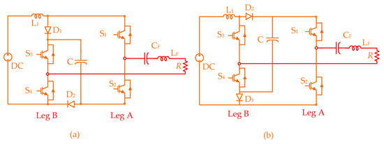
Figure 9.
Four-switch quasi-switched boost inverter (FS-qSBI) topology (a) Type 1; (b) Type 2.
The FS-qSBI has the benefits of reduced switches than traditional qSBI. One of the major drawbacks of the FS-qSBI topology is the low-frequency ripple issue. This impacts the system stability and increases voltage stress. It can be suppressed by the utilization of large passive elements. The additional passive components result in increased size, weight, and cost of the system. To avoid this, a damping scheme is presented for the four switch qSBI in [42] to overcome the low frequency ripple issue. In this control scheme, the low-frequency ripple portion is extracted and added to the ST duty ratio D. This damping scheme improves the stability of the system and has reduced voltage stress on the components. In [43], active power decoupling (APD) integrated FS-qSBI is presented to mitigate low frequency ripple problem. Figure 10 presents the four-switch qSBI topology with APD. A dependent buck-type APD network is added to the FS-qSBI with auxiliary inductor Ls and capacitor Cs. The operation of the APD topology is coupled to the switches of leg A and depends on the operation of the inverter. The ripple energy is deviated from the DC-link capacitor C and redirected to the capacitor Cs by the auxiliary inductor Ls. The auxiliary inductor also filters the output current and decouples the ripple current and load current. Compared to the FS-qSBI, the APD FS-qSBI has reduced ripples and improved load voltage. Additionally, the size of the passive components is reduced.
Figure 10.
Four-switch quasi-switched boost inverter topology with active power decoupling.
In [44], two qSBI topologies with an active impedance-source network are presented as high gain qSBI with a novel PWM technique to achieve high voltage gain. Figure 11b presents the switched capacitor qSBI topologies derived from the embedded qSBI by adding a capacitor and diode. This configuration offers high voltage gain and reduced voltage stress on the devices. The inverter structure can be further extendable to N-Cell to increase the voltage gain. The N-Cell can be obtained by connecting a capacitor and diode in cascade to the qSBI structure. This configuration reduced the ST voltage and current stress on the components. Therefore, it enables the utilization of low voltage rating components and results in improved efficiency, reduced size, and power losses.
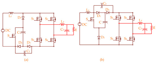
Figure 11.
Switched-capacitor based qSBI topologies (SC-qSBI) (a) Type 1; (b) Type 2.
The coupled-inductor based impedance source topologies are attracting lot of research interests and variety of applications [15] due to their benefits of high gain with reduced passive components and low cost. Two coupled-inductor derived qSBI topologies with control strategy based on space vector pulse width modulation (SVPWM) technique are presented in [45]. The benefits of CI-qSBI topologies are high boost ability and low voltage stress on the components. High voltage gain can be achieved by varying the duty cycle and turns ratio of the coupled inductor. The voltage gain of the presented topologies can be further improved by adding a boost unit. The coupled-inductor qSBI topologies are derived by adding a coupled-inductor, capacitor, and diode to the qSB network. Figure 12a,b presents two coupled-inductor qSBI topologies. In the coupled-inductor qSBI Type 1, the input ground node is directly connected to the negative node of the inverter bridge and in Type 2, the ground is not directly connected to the negative node.
Figure 12.
Coupled-inductor based quasi-switched boost inverter topologies (CI-qSBI). (a) Single cell CI-qSBI Type 1; (b) Single cell CI-qSBI Type 2.
The presented topologies can be extended by cascading cells to improve the voltage gain. Each cell consists of a pair of capacitor and diodes with a winding N. Figure 13 presents the extended coupled-inductor qSBI.
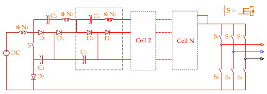
Figure 13.
Extended coupled-inductor based quasi-switched boost inverter topologies (CI-qZSI).
A three-phase qSBI topology with fault-tolerant solution is shown in Figure 14a. The fault-tolerant qSBI [46] is derived by adding three TRIACS between the source and output terminals. During an open circuit failure, the output power of the converter decreases and leads to high distortion in the AC current. To mitigate this problem, the three additional TRIACS will reconfigure the circuit and allows the continuous operation. For example, if there is an open-circuit failure in the Switch S6, then the TRIAC 3 turns ON and disconnect the control over the third-leg. The reconfigured circuit behaves like a four-switch three-phase qSBI, as shown in Figure 14b, and the inverter will operate with two-legs. The TRIAC 3 connects the third phase to the input source. During fault-tolerant mode, the qSBI operates in the boost mode. This reconfiguration minimizes the impacts of the open-circuit failure.
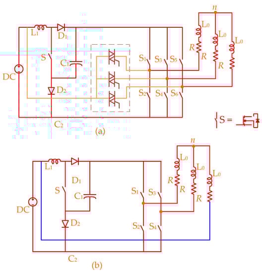
Figure 14.
Fault-tolerant three-phase quasi-switched boost inverter. (a) Normal operation; (b) Reconfigured circuit.
The isolated DC–DC converters are widely used for high step-up applications because of their capability to provide high voltage gain and galvanic isolation between the source side and the output side. The boost type isolated DC–DC converters are based on two stage power conversion and require a transformer and voltage lift techniques to achieve high voltage gain. The impedance source based isolated DC–DC converters were presented in [47,48,49,50,51,52] with single-stage power conversion ability and high voltage gain with the cost of increased passive components size and count. In order to overcome this drawback, an isolated high step-up DC–DC converter is presented in [53] with a qSB network, transformer and voltage double rectifier. The qSB based isolated DC–DC converter provides galvanic isolation and converts low voltage DC input to stabilized DC voltage. Figure 15 presents the isolated qSB (IqSB) DC–DC converter. The switching pattern of the IqSB DC–DC converter is obtained by comparing two reference signals Vref and (1-Vref) with a high frequency triangular waveform. The ST signal is generated by comparing a constant reference voltage of the range (Vref,1) with a triangular waveform of 180-degree phase-shift and then inserted into the control signals of the switches using logic gates OR. The presented topology can operate either in the open-circuit or short-circuit mode without any damage to the converter. The benefits of the IqSB DC–DC are continuous input current and reduced turns ratio of the isolated transformer. In comparison to the qZS derived isolated topologies, the IqSB DC–DC converter has few passive components, resulting in reduced size and cost of the converter. Additionally, the primary and secondary voltage waveforms of the transformer remain unchanged for variable ST duty cycle and the zero-time interval is independent on the ST time interval. The IqSB converter is well suitable for applications like distributed power generation where the high stabilized DC output voltage and galvanic isolation requirements take place.
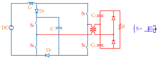
Figure 15.
Isolated high step-up quasi-switched boost inverter.
In general, the grid-connected inverters can be classified into two categories as galvanic isolation system and transformerless system. The galvanic isolation systems require either a low-frequency transformer in the AC side or a high frequency transformer in the DC side to provide isolation between the PV system and grid. This isolation limits the common mode current and ensures that no direct current is injected into the grid and thus provides safety. However, the presence of the transformer reduces the system efficiency and also increases the size and cost of the system. The transformerless system overcomes the abovementioned drawback by elimination of the transformer. Among the two, the transformerless based solutions have received more attention due to their high efficiency, reduced size, lightweight, and cost effectiveness. One of the major drawbacks of the transformerless PV inverter is the generation of common-mode voltage (CMV) during operation. The CMV with high frequency and magnitude leads to leakage current on the stray capacitors. This leakage current increases the power losses and fastens the PV panel degradation. The leakage current can be reduced by utilizing CMV reduction techniques like modifying the PWM strategy and system topology reconfiguration. The system reconfiguration involves the structural modification of the active and passive components or by the utilization of a CMV passive filter. The CMV passive filter blocks the leakage current without changing the CMV level. The drawbacks of the system reconfiguration method include complex control, increased power losses and cost. Several modified carrier-based and PWM strategies were developed over the years without changing the hardware and components. The modified carrier solutions reduce the high frequency harmonics of CMV and common-mode current (CMC). However, they have the drawbacks of high output voltage THD value and software complications. Some of the popular modulation-based CMV reduction techniques are remote state space vector PWM (RS-SVPWM), active zero state space vector PWM (AZS-SVPEM), and near state space vector PWM (NS-SVPWM) method [54,55,56,57]. The qSBI topology has the drawback of high amplitude common-mode voltage due to ST state insertion. Because of this CMV generation, the qSBI topologies are not favored for transformerless PV system applications. To overcome the effects of leakage current, a modified two-switched qSBI topology is presented with two active zero state SV-PWM (AZSTPVM) in [58]. The 2S-qSBI derived from the embedded qSBI by replacing the diode DA with an additional Switch S2 is presented in [33] with stable DC-link voltage during NST state. Figure 16a,b shows the 2S-qSBI Type 1 and Type 2 configurations. In 2S-qSBI Type 1 configuration, the switches S1 and S2 have common drain and in 2S-qSBI Type 2, the switches S1 and S2 have common source. Similar to the qSBI, the 2S-qSBI has two operating modes as ST state and NST state. In the ST state, at least one leg of the H-bridge is turned ON and in the NST state, the 2S-qSBI works like conventional VSI. The 2S-qSBI has the benefits of continuous input current, wide range of input voltage regulation and reduced system size.
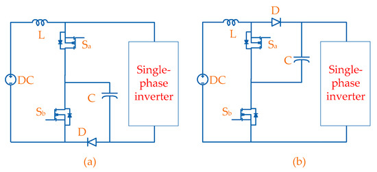
Figure 16.
2-Switch quasi-switched boost inverter (a) Type 1; (b)Type 2.
In the modified 2S-qSBI, an additional inductor is inserted into the negative input of the source side as shown in Figure 17a. The modified 2S-qSBI has two operation states as ST and NST state. In the ST state, switch S2 is turned ON and the ST pulses are provided to the Switch S2 along with the H-bridge inverter switches(S1-S4). In NST state, switch S2 is turned OFF and the switch S1 is turned ON. The modified 2S-qSBI is presented with two modulation techniques namely, AZSI-SVM2 and AZSI-SVM4 based on the AZ-SVM technique. In the AZSI-SVM2 method, the total ST state is divided into two parts per one control cycle with time interval as TST/2 and in AZSI-SVM4, the ST state is divided into four parts per one control cycle with time interval as TST/4. Among the two AZST-SVM methods, the AZST-SVM2 has better efficiency with reduced switching losses and AZST-SVM4 has lower input current ripples. The RMS leakage current of the M2S-qSBI with AZST-SVM2 and AZST-SVM4 technique falls in the range of the permissible range according to the standard VDE 0126-1-1 [59]. The equivalent and simplified common mode model of the modified 2S-qSBI is shown in Figure 17b,c.
Figure 17.
(a) Two switched quasi-switched boost inverter; (b) Equivalent model of the common-mode model of modified 2 Switch-qSBI topology; (c) Simplified model of the common-mode model of modified 2 Switch-qSBI.
In [60], two high gain qSBI (HG-qSBI) topologies are presented with improved voltage gain obtained by inserting a capacitor and inductor to the traditional qSBI. The HG-qSBI has the benefits of high voltage gain and low voltage stress on the components. Compared to the SL-qSBI and HB-qSBI, the HG-qSBI has the lowest power losses. However, the weight and cost of the HG-qSBI are higher compared to the similar qSBI topologies and also suffers from hard switching. The HG-qSBI topologies are presented in Figure 18. To overcome the aforementioned drawbacks, a modified modulation technique based on the combination of PWM technique and phase shift was proposed for the HG-qSBI in [61]. The soft switching is achieved by the phase difference of α radian between the gating signals. The gating signals of the switched S3 and S4 are phase-shifted by a α radian compared to the gating signals of switches S1 and S2. This modified switching algorithm provides soft switching and better voltage gain with low voltage stress on the capacitors.
Figure 18.
High-gain quasi-switched boost inverter topologies (a) Type 1; (b) Type2.
The voltage multiplier cells are widely used in the power conversion process to produce higher voltage gain and to reduce stress on the components. A voltage multiplier cell based qSBI (VMC-qSBI) was presented in [62] with a new PWM technique to achieve high voltage gain and reliability with high modulation index. Figure 19 shows the VMC-qSBI. A very high voltage gain conversion can be achieved by utilizing multi-voltage multiplier cells. The control signal for the active impedance network switch is obtained by comparing a fixed voltage signal with a double frequency triangular waveform. The ST signal is produced by comparing another fixed voltage signal with the double frequency triangular waveform and then inserted into the inverter switched using OR logic gates.
Figure 19.
Single cell voltage multiplier cell based quasi-switched boost inverter.
This configuration can be extended to N-number of cells by adding VMC as shown in Figure 20. Compared to other active impedance source inverters, the VMC-qSBI has continuous input current with low input ripple and ST immunity. Low THD can be achieved by using high modulation index. The drawbacks of the VMC-qSBI are high voltage stress on the components and increased component count. The VMC-qSBI topologies are well suitable for applications like the PV generator and wind power.
Figure 20.
N-cell voltage multiplier cell based quasi-switched boost inverter.
Table 1 presents the comparison of various qSBI derived topologies based on the most important parameters. Figure 21 and Figure 22 give the visual representations of the boost factor and voltage gain dependencies for the enlisted topologies. The components quantity required for each topology could be evaluated from the Figure 23.

Table 1.
Comparison of quasi-switched boost inverter topologies.
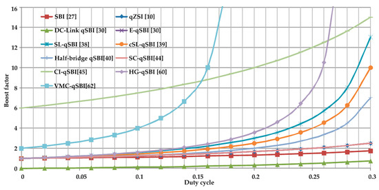
Figure 21.
Boost factor as a function of the duty cycle for the topologies enlisted in Table 1.
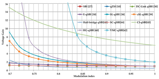
Figure 22.
Voltage gain as a function of the modulation index for the topologies enlisted in Table 1.
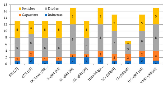
Figure 23.
The components required for the topologies enlisted in Table 1.
The interleaving techniques are gaining a lot of popularity in recent years due to their high efficiency in wide power range applications and reduced conduction losses achieved by splitting the current paths. The multiphase interleaving techniques provide enhanced power density, high voltage gain, reduced current ripples, and passive components. In [63], an interleaved topology based on the qZSI (IqZSI) is presented with a control technique based on the combination of phase-shifted PWM and SBC Technique. The presented topology combines the benefits of qZSI topology and VSI with interleaved parallel legs. The IqZSI topology has higher power density, smaller output filter, and reduced output THD. The drawbacks of this approach are reduced boost factor and poor DC-Link utilization. To overcome these drawbacks, IqZSI is presented with a modified modulation technique based on the MBC technique. In a single-phase system, the direct application of the MBC technique generates high voltage distortions and DC-Link voltage ripples due to the variable width of the ST states. Due to this, a modified MBC technique with smooth variable DS is presented in [64]. The modified MBC based IqZSI topology has better DC-Link voltage stabilization and higher boost factor. The presented technique has the drawbacks of worse THD compared to the SBC technique. In [65], IqZSI is presented with APD configuration resulting in reduction in the passive components. The IqZSI is extended to PV application with different control approaches and modulation techniques in [66,67,68]. Figure 24a shows the interleaved qSBI for single-phase application (IqSBI). In [69], the IqSBI topology is presented with a modified MBC technique and quasi-sinusoidal modulation (qSM) technique. The IqSBI and AqZSI configurations are obtained by replacing the qZSI topology in [64]. In modified MBC technique, the control states for the switches in the top and bottom inverter are generated by comparing two sinusoidal reference signals of 180° phase-shift with two carrier signals of 90° phase-shift. The top and bottom envelopes are generated by the maximum and minimum of the two sinusoidal reference signals and smoothen by the next auxiliary signals. The ST states are generated based on the auxiliary signals. They are inserted into the control signal of the top and bottom inverter switches by using logic gate function OR. The control signals for the switch SA and SB are generated by comparing a constant voltage signal with a double frequency carrier signal. To improve the boosting ability, a qSM technique is presented for the interleaved topologies in [69]. In [70], qSM technique is presented for the single-phase qZSI. In qSM strategy, the control signal for the top and bottom inverter can be generated by comparing two reference signals with two carrier signals of 90° phase-shift. The reference signals are triggered by minimum of the reference signal with a constant voltage signal, as shown in Figure 24b. The control signal for the Switch SA and SB are generated by comparing a constant voltage signal with double frequency carrier signal. The interleaved topologies perform better using qSM technique compared to the modified MBC modulation technique. The IqSBI has the advantage of reduced passive components and better performance compared to IqZSI for lower power applications.
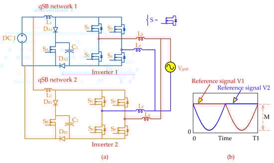
Figure 24.
(a) Interleaved quasi-switched boost inverter topology; (b) Reference signal waveform.
The multilevel inverters are gaining a lot of research interests due to the increasing power-scale demands. The major benefits of multilevel inverters include lower electromagnetic interference, improved output waveforms, allows use of smaller size filter, and lower THD. Among the multilevel inverter structures, the cascaded H-bridge inverters has the benefits of high reliability, reduced filter size, and higher output voltage compared to the neutral point clamped (NPC) and flying capacitor (FC) type topologies. The cascaded H-bridge (CHB) inverter utilize separate sources and cascade multiple H-bridge modules to generate the total output voltage. The CHB inverter has the advantage of high reliability due to its modular structure and reduced output filter size. However, the CHB inverter has the drawback of limited DC–AC power conversion and short-circuit issues. Several qZSI derived CHB inverter topologies were presented [71,72,73,74] to overcome the problems of the CHB-VSI and provide single-stage power conversion. The CHB-qZSI utilize multiple qZSI network with large number of passive components and results in increased size and cost of system.
A quasi-CHB five-level boost inverter (qCHB-FLBI) is presented in [75] with a phase-shifted PWM (PS-SPWM) technique. Compared to the CHB-qZSI, the qCHB-FLBI topology have the benefits of reduced inductor current ripples, lower output current THD, and passive components. The qCHB-FLBI utilize two quasi-boost modules with separate DC sources and an inductor filter to produce five-level output voltage. Each quasi-boost module consist of one inductor, capacitor, two diodes and four switches. Figure 25 presents the quasi-cascaded H-bridge five-level boost inverter.
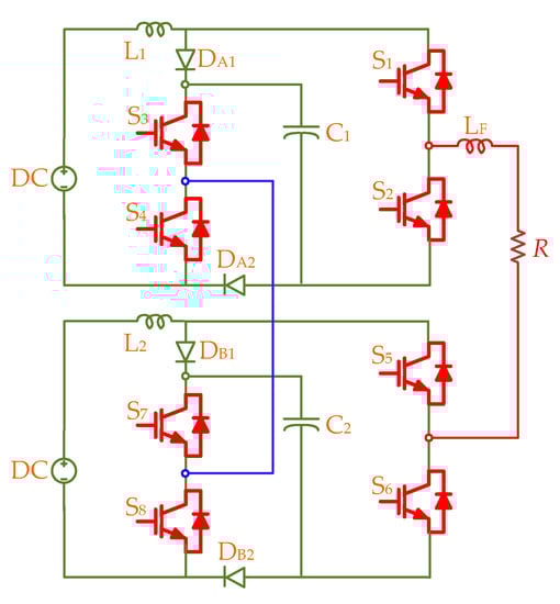
Figure 25.
Quasi-cascaded H-bridge five-level boost inverter.
A single-phase CHB based on the qSBI topology is presented in [76,77] with an improved phase-shifted sinusoidal PWM control strategy to generate the DC-link voltage. The single phase cascaded qSBI utilize two qSBI networks connected to separate DC sources with two H-bridge modules and an inductive filter. The output voltage of the cascaded qSBI can be extended by cascading multiple qSBI networks. The control signals for the switches in each H-bridge are generated separately using two triangular waveforms of phase shifted in 90-degree. The control signal for the qSB network switch is generated by comparing a constant voltage signal with triangular waveform of half amplitude and double frequency of another triangular waveform. This control signal is then inserted into the control signals of H-bridge switches using logic gates OR to generate the ST states. Each H-bridge module has three output voltage level and the output of the cascaded qSBI system is the total sum of the H-bridge module outputs. The CHB-qSBI utilize reduced number of passive components than the CHB-qZSI and offers compact system well suitable for low power applications. Figure 26 shows the single-phase cascaded H-Bridge qSBI presented in with two DC sources and two qSBI modules.
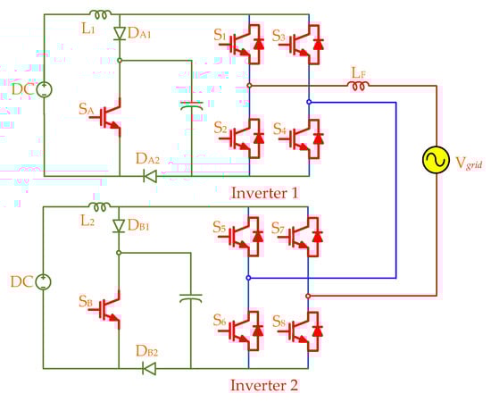
Figure 26.
Single phase cascaded H-bridge qSBI topology.
In [78], a three-phase cascaded H-bridge qSBI is presented as an alternative solution to the impedance source based cascaded H-bridge inverter. The three-phase CHB-qSBI utilizes six qSBI modules with six separate DC sources and produces five-level output phase voltage. Compared to the three-phase CHB-qZSI, the presented configuration has fewer passive components resulting in reduced size and power losses. The CHB-qSBI has drawbacks of higher voltage stress across the passive components and limitations of using a small modulation value to achieve high voltage gain because of the conventional PWM technique. Figure 27 presents the three-phase CHB-qSBI topology.
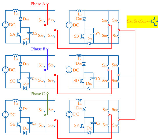
Figure 27.
Three-phase cascaded H-bridge qSBI topology.
A cascaded three-phase five-level inverter is presented in [79] with a PWM technique to improve the modulation index. The CHB-qSBI overcomes the voltage imbalance problems of the traditional CHB inverter by the implementation of an improved phase-shifted sinusoidal PWM strategy. This improved phase-shifted SPWM strategy overcomes the voltage imbalance problems by utilization of the indirect DC-Link voltage control method by controlling and stabilizing the capacitor voltage. Compared to the CHB qZSI, the presented topology has the advantage of reduced size and cost. Additionally, the CHB qSBI has lower output voltage THD and stable operation in both balanced and unbalanced input voltage modes. In [80], a DC-Link quasi-switched boost cascaded multilevel inverter (DqSB-CMI) is presented for grid-tied applications. It utilizes three DC sources connected separately to three DqSB modules with an inductor filter. Figure 28 presents the mentioned DqSB-CMI. It utilizes a modified PWM method presented in [37]. The DqSB-CMI has the benefits of active and reactive power control capability, reduced voltage stress on the components and overcomes DC-Link voltage imbalance problems. The DqSB-CMI based distributed generation systems have reduced volume and weight compared to ZSI/qZSI based systems.
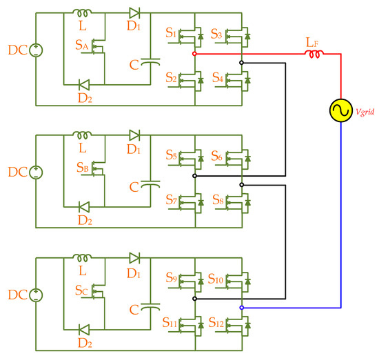
Figure 28.
DC-Link qSBI cascaded multilevel inverter topology.
The VSIs are widely used in the distributed power systems for DC–AC power conversion. To achieve higher AC output voltage conversion, the VSI requires an additional two-level and three-level DC–DC converter to boost the low input DC voltage. To overcome the two-stage power conversion and ST issues of three-level boost inverters, impedance-source network integrated multilevel inverters were presented with single-stage power conversion and ST immunity [81]. The 3L-ZSI [82] utilize two ZS networks, two isolated DC sources and a three-level NPC inverter. The presence of two LC networks increases the volume and cost of the inverter. Three phase 3L-NPC inverter with single Z-source network was reported in [83] derived by connecting the midpoint of the DC sources with the neutral point of the NPC inverter. The ZSI based 3L-NPC has the drawbacks of high component stress, discontinuous input current and low voltage gain. To overcome aforementioned drawbacks, quasi-Z-source based 3L-NPC multilevel inverter is presented in [84] with continuous input current. In [85], a three-level LC-switching based voltage boost NPC inverter is presented. The 3L LC-switching based voltage boost NPC inherits the advantages of quasi-Z-source based 3L-NPC multilevel inverter with reduced passive components. The gating signals for the switches are generated using unipolar PWM technique. Figure 29 presents the 3L LC-switching voltage boost NPC inverter.
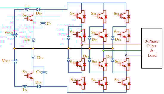
Figure 29.
Three level LC-switching voltage boost NPC inverter.
In [86], a switched-capacitor qSB based NPC multilevel inverter is presented with multi-carrier level-shifted PWM technique. The SC-qSB NPC multilevel inverter can be further extended by adding multi-cell switched-capacitor cell arrangement to achieve high voltage gain. The control signals for the switches are generated by comparing three modulating signals of 120° phase shift with two triangular signals and two ST reference signals. The gating signals of the switches SP and SN are generated by comparing the ST signals and two triangular signals. The gating signals of the inverter leg switches are generated by comparing the modulating waveforms with triangular waveforms and then the ST signals are inserted using logic gate OR. Figure 30 presents switched-capacitor qSB based NPC multilevel inverter topology.
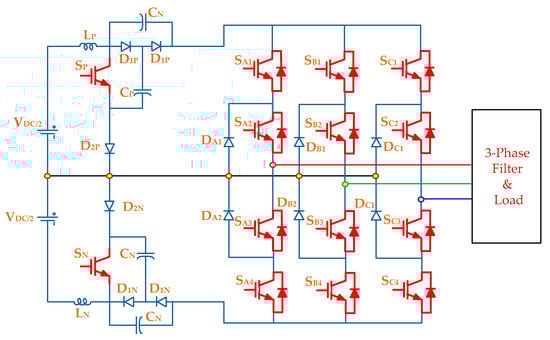
Figure 30.
Switched-capacitor qSB based neutral point clamped multilevel inverter.
A three-phase 3L qZSI is presented in [87] with improved current profile and reduced component size. The three-phase 3L qZSI comprises of a 3L T-Type inverter and two symmetrical qZS network. However, the large passive components in the impedance source based 3L inverters results in increased size, weight and cost of the inverter. The qSBI derived topologies are gaining a lot of interest in the distributed generation applications because of their reduced size and cost.
In [88], a three-level quasi-switched boost T-type inverter (3L-qSBT2I) is presented with anti-series switches configuration. Figure 31 shows the three-level qSB T-type inverter. The 3L-qSBT2I with anti-series configuration is derived by incorporating qSB network to the conventional 3L T-Type inverter front structure. The neutral point is connected to the load using three bidirectional switches. Each bidirectional switch consists of two switches connected in series configuration. The advantage of 3L-qSBT2I include improved voltage gain, very low input current ripple, and ST immunity.
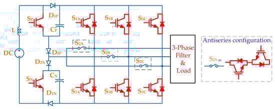
Figure 31.
3L qSBI T-Type inverter topology with anti-series configuration switches.
In [89], a controlled diode bridge clamped qSB three-level inverter is presented. Figure 32 shows the three-level qSB T-Type inverter with controlled diode bridge clamp (CDBC) switch configurations. The conventional T-Type three-phase inverter utilizes three bidirectional switches with six IGBTs, made with an anti-series configuration of two IGBTs per phase leg. In the CDBC three-level inverter, the DC bus midpoint of each phase leg is connected by a bidirectional switch constructed by the combination of one IGBT and four diodes. The CDBC qSB-3L has the drawbacks of IGBT switch operating at the double frequency of the switches in phase legs. Additionally, the presence of one more diode in the conduction path results in power loss. In [90], a SVPWM scheme with reduced inductor current is presented for 3L-qSBT2I. This modulation scheme utilizes high value of modulation index by maintaining constant ST duty cycle. The presented technique has the advantage of improved voltage gain achieved by controlling the duty cycle of the two switches. A fault-tolerant 3L-qSBT2I is presented in [91] with ability to operate in normal and fault modes. In [87], a fault tolerant Z-source inverter is presented with a PWM technique controlled by ST duty cycle and modulation index M. During the fault mode, the inverter is operated with low modulation index and high ST duty cycle. This operation reduces the output quality of the inverter and result in high ST currents, increased voltage stress and power losses. To overcome the mentioned drawbacks, a fault-tolerant PWM control technique based on low ST duty-cycle and high modulation index is presented in [92]. The fault tolerant 3L-qSBT2I has the benefits of reduced input current ripple and voltage stress on the switches and capacitors. In [93,94], SVM technique with CMV reduction is presented for 3L-qSBT2I with the features of reduced CMV, low inductor current ripple, ST immunity, and allows use of high modulation index. In the conventional SVM CMV reduction technique [95], the reference vector is generated using the large, medium and zero vectors. In this technique, the reference vectors are generated using medium and zero vectors.
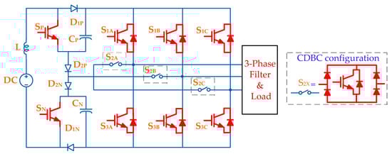
Figure 32.
3L qSBI T-Type inverter with CDBC configuration switch.
In [96], a three level DC-Link qSB T-Type inverter is presented. The 3L-DqSBTI incorporates a DC-Link qSBI topology with 3L T-Type inverter. The 3L-DqSBTI utilize the SVPWM technique with enhanced modulation index. The 3L-DqSBT2I has a better voltage gain and boost factor compared to the conventional 3qSB T-Type inverter. The 3L-DqSBT2I has reduced voltage stress on the components and reduced CMV magnitude. The CDBC configuration has the advantage of three less IGBT switches and its associated gate driver and circuit elements compared to the conventional T-Type. Figure 33 presents the three-level DC-Link qSB T-Type inverter. Table 2 presents the comparison of qSB derived configurations based on the most important parameters. The components quantity required for each configuration could be evaluated from the Figure 34.
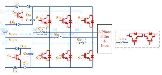
Figure 33.
DC-Link qSBI T-Type inverter topology.
Table 2.
Comparison of quasi-switched boost inverter configurations.
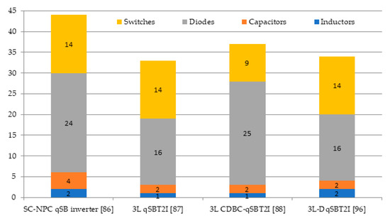
Figure 34.
The components required for the configurations enlisted in Table 2.
4. Discussion
Efficiency is an important factor to be considered in the selection of the power converter. The total losses in the converter have direct impact on the efficiency of the system. The major contributors of the total power losses in converters are switches, inductors, and diodes. Compared to the qZSI topology, the basic qSBI topologies has reduced passive components resulting in lower inductor loss and power switch loss. Therefore, the qSBI topology has lower power loss than the qZSI. Additionally, the parasitic system effect in qZSI is higher than qSBI. The qSBI has the same features of the qZSI with better efficiency in low and medium power applications. The drawback of the qSBI is high voltage stress in capacitor and the low frequency ripple issue. The qSBI is not preferred for high voltage gain applications where high boost voltage is required because of the high voltage stress on the components and switches. The SL-qSBI has high power loss and input ripples. The cSL-qSBI offers high power density and better efficiency than the switched inductor based ZSI and qZSI topologies at low realization cost and reduced components. The SC-qSBI has higher efficiency compared to the SL-qSBI. However, the voltage stress in the qSB network switch is high and also the voltage gain is not up to the desired level. A 500W prototype of SC-qSBI in grid-connected and stand-alone mode operation is presented in [44] with efficiency of 91.5%. The FS-qSBI derived by combining the ST and conventional inverter operation by removing the extra switch has improved efficiency. Similar to the qSBI, the FS-qSBI also suffers from low frequency ripple issue. To mitigate the low frequency ripple issue in FS-qSBI, low frequency ripple damping scheme and APD configuration could be used. The CI-qSBI has high voltage gain and reduced stress on the components. In addition, the voltage gain can be improved by adjusting the duty cycle and turns ratio without operating the circuit in higher duty cycle. A 200W prototype of the CI-qSBI is presented in [45] with efficiency of 93.1%. The qSBI derived configurations have reduced components and enhanced efficiency compared to the impedance source derived configurations. The qSBI derived configurations are preferable for low and medium power applications due to their reduced size, weight and cost. The voltage multiplier cell based qSBI topologies are suitable for renewable energy related applications such as wind power. The T-Type qSBI topologies are suitable for applications like UPS, motor drives, and photovoltaic systems. The cascaded qSBI topologies are well suitable for distributed generation systems. Several fault-tolerant techniques and common-mode-voltage regulation methods are introduced for the qSBI family to improve the efficiency and reliability. The efficiency of the converter can be further enhanced by the utilization of high performance MOSFET switches. Future research could be directed towards bidirectional operation, utilization of new semiconductor devices, and implementations in emerging applications related to renewable energy-based systems, particularly autonomous power supply PV-based systems.
5. Conclusions
A review of qSBI and their topological variations has been presented with comparison and analysis based on the most important parameters. Several derived topologies were developed to improve the moderate voltage gain of the qSBI. The benefits and drawbacks of each configuration are presented and an overview comparison of the qSB derived topologies is summarized. The qSBI derived topologies have the benefit of enhanced voltage gain with reduced voltage stresses on the components and replace the impedance source converter in low power applications. The efficiency of the converter can be further enhanced by the utilization of high performance MOSFET switches. Future research could be directed towards bidirectional operation, utilization of new semiconductor devices and implementations in emerging applications related to renewable energy-based systems including autonomous power supply photovoltaic based systems.
Author Contributions
Conceptualization J.G.N.B., O.H., methodology D.V.; software, J.G.N.B., S.S.; validation M.-K.N.; formal analysis, J.G.N.B., A.S.; resources, O.H., M.-K.N.; writing-original draft preparation, J.G.N.B.; writing-reviewing and editing, S.S., O.H., D.V., M.-K.N., A.S.; visualization, J.G.N.B., S.S.; supervision, A.S.; project administration, D.V.; funding acquisition, S.S., D.V. All authors have read and agreed to the published version of the manuscript.
Funding
This research work was financed in part by the Ministry of Education and Science of Ukraine, grant number 0120U101554. It was partially supported by the Estonian Research Council grant PRG1086 and in part by the Estonian Centre of Excellence in Zero Energy and Resource Efficient Smart Buildings and Districts, ZEBE, grant 2014-2020.4.01.15-0016 funded by the European Regional Development Fund.
Conflicts of Interest
The authors declare there are no conflict of interests.
References
- Peng, F.Z. Z-source inverter. IEEE Trans. Ind. Appl. 2003, 39, 504–510. [Google Scholar] [CrossRef]
- Cha, H.; Peng, F.Z.; Yoo, D.-W. Distributed Impedance Network (Z-Network) DC–DC Converter. IEEE Trans. Power Electron. 2010, 25, 2722–2733. [Google Scholar] [CrossRef]
- Hossein, S.; Sedaghati, F.; Sarhangzadeh, M. Improved power quality three phase AC-DC converter. In Proceedings of the 2010 International Conference on Electrical Machines and Systems, Incheon, Korea, 10–13 October 2010; pp. 148–153. [Google Scholar]
- Fang, X.; Cao, M.; Chen, Z. Z-source AC-DC-AC converter for mining applications. In Proceedings of the 2010 International Conference on Electrical Machines and Systems, Incheon, Korea, 10–13 October 2010; pp. 44–47. [Google Scholar]
- Fang, X.P.; Qian, Z.M.; Peng, F.Z. Single-phase Z-source PWM AC-AC converters. IEEE Power Electron. Lett. 2005, 3, 121–124. [Google Scholar] [CrossRef]
- Nguyen, M.K.; Jung, Y.G.; Lim, Y.C. Single-Phase Z-Source AC/AC converter with wide range output voltage operation. J. Power Electron. 2009, 9, 736–747. [Google Scholar]
- Peng, F.Z.; Joseph, A.; Wang, J.; Shen, M.; Chen, L.; Pan, Z.; Ortiz-Rivera, E.; Huang, Y. Z-Source Inverter for Motor Drives. IEEE Trans. Power Electron. 2005, 20, 857–863. [Google Scholar] [CrossRef]
- Huang, Y.; Shen, M.; Peng, F.Z.; Wang, J. ZZ-Source Inverter for Residential Photovoltaic Systems. IEEE Trans. Power Electron. 2006, 21, 1776–1782. [Google Scholar] [CrossRef]
- Peng, F.; Yuan, X.; Fang, X.; Qian, Z. Z-source inverter for adjustable speed drives. IEEE Power Electron. Lett. 2003, 1, 33–35. [Google Scholar] [CrossRef]
- Anderson, J.; Peng, F. Four quasi-Z-Source inverters. In Proceedings of the 2008 IEEE Power Electronics Specialists Conference, Rhodes, Greece, 15–19 June 2008; pp. 2743–2749. [Google Scholar] [CrossRef]
- Vinnikov, D.; Roasto, I. Quasi-Z-Source-Based Isolated DC/DC Converters for Distributed Power Generation. IEEE Trans. Ind. Electron. 2010, 58, 192–201. [Google Scholar] [CrossRef]
- Liu, Y.; Ge, B.; Peng, F.Z.; Haitham, A.R.; Almeida, A.; Ferreira, F.J.T.E. Quasi-Z-Source inverter based PMSG wind power generation system. In Proceedings of the 2011 IEEE Energy Conversion Congress and Exposition, Phoenix, AZ, USA, 17–22 September 2011; pp. 291–297. [Google Scholar] [CrossRef]
- Cintron-Rivera, J.G.; Li, Y.; Jiang, S.; Peng, F.Z. Quasi-Z-source inverter with energy storage for pho-tovoltaic power generation systems. In Proceedings of the 2011 Twenty-Sixth Annual IEEE Applied Power Electronics Conference and Ex-position (APEC), Fort Worth, TX, USA, 6–11 March 2011; pp. 401–406. [Google Scholar] [CrossRef]
- Chub, A.; Vinnikov, D.; Jalakas, T. Galvanically isolated quasi-Z-source DC-DC converters with combined energy transfer for renewable energy sources integration. In Proceedings of the 2015 IEEE International Conference on Industrial Technology (ICIT), Seville, Spain, 17–19 March 2015; pp. 2896–2900. [Google Scholar] [CrossRef]
- Vinnikov, D.; Chub, A.; Liivik, E.; Kosenko, R.; Korkh, O. Solar Optiverter—A Novel Hybrid Approach to the Photovoltaic Module Level Power Electronics. IEEE Trans. Ind. Electron. 2018, 66, 3869–3880. [Google Scholar] [CrossRef]
- Siwakoti, Y.P.; Peng, F.Z.; Blaabjerg, F.; Loh, P.C.; Town, G.E. Impedance-Source Networks for Electric Power Conversion Part I: A Topological Review. IEEE Trans. Power Electron. 2015, 30, 699–716. [Google Scholar] [CrossRef]
- Siwakoti, Y.P.; Peng, F.Z.; Blaabjerg, F.; Loh, P.C.; Town, G.E.; Yang, S. Imped-ance-source networks for electric power conversion part II: Review of control and modulation techniques. IEEE Trans. Power Electron. 2014, 30, 1887–1906. [Google Scholar] [CrossRef]
- Liu, Y.; Abu-Rub, H.; Ge, B. Z-Source/Quasi-Z-Source Inverters: Derived Networks, Modulations, Controls, and Emerging Applications to Photovoltaic Conversion. IEEE Ind. Electron. Mag. 2014, 8, 32–44. [Google Scholar] [CrossRef]
- Barath, J.G.N.; Soundarrajan, A.; Stepenko, S.; Padmanaban, S.; Prystupa, A.; Bolotov, M. Review of Extended Boost qZSI Topologies for Single Phase Applications. In Proceedings of the 2019 IEEE 60th International Scientific Conference on Power and Electrical Engineering of Riga Technical University (RTUCON), Riga, Latvia, 7–9 October 2019; pp. 1–8. [Google Scholar] [CrossRef]
- Ellabban, O.; Abu-Rub, H. Z-Source Inverter: Topology Improvements Review. IEEE Ind. Electron. Mag. 2016, 10, 6–24. [Google Scholar] [CrossRef]
- Husev, O.; Shults, T.; Vinnikov, D.; Roncero-Clemente, C.; Romero-Cadaval, E.; Chub, A. Comprehensive Comparative Analysis of Impedance-Source Networks for DC and AC Application. Electronics 2019, 8, 405. [Google Scholar] [CrossRef]
- Panfilov, D.; Oleksandr, H.; Frede, B.; Janis, Z.; Kamal, K. Comparison of three-phase three-level voltage source inverter with intermediate dc–dc boost converter and quasi-Z-source inverter. IET Power Electron. 2016, 9, 1238–1248. [Google Scholar] [CrossRef]
- Wolski, K.; Zdanowski, M.; Rabkowski, J. High-frequency SiC-based inverters with input stages based on quasi-Z-source and boost topologies—Experimental comparison. IEEE Trans. Power Electron. 2019, 34, 9471–9478. [Google Scholar] [CrossRef]
- Gadalla, B.; Schaltz, E.; Siwakoti, Y.P.; Blaabjerg, F. Thermal performance and efficiency investigation of conventional boost, Z-source and Y-source converters. In Proceedings of the 2016 IEEE 16th International Conference on Environment and Electrical Engineering (EEEIC), Florence, Italy, 7–10 June 2016; pp. 1–6. [Google Scholar] [CrossRef]
- Vinnikov, D.; Chub, A.; Roasto, I.; Liivik, L. Multi-mode quasi-Z-source series resonant DC/DC con-verter for wide input voltage range applications. In Proceedings of the 2016 IEEE Applied Power Electronics Conference and Exposition (APEC), Long Beach, CA, USA, 20–24 March 2016; pp. 2533–2539. [Google Scholar] [CrossRef]
- Oleksandr, H.; Vinnikov, D.; Roncero-Clemente, C.; Chub, A.; Romero-Cadaval, E. Single-Phase String Solar qZS-based Inverter: Example of Multi-Objective Optimization Design. IEEE Trans. Ind. Appl. 2020, 57, 3120–3130. [Google Scholar]
- Mishra, S.; Adda, R.; Joshi, A. Inverse Watkins–Johnson Topology-Based Inverter. IEEE Trans. Power Electron. 2012, 27, 1066–1070. [Google Scholar] [CrossRef]
- Nguyen, M.-K.; Lim, Y.-C.; Choi, J.-H.; Choi, Y.-O. Trans-switched boost inverters. IET Power Electron. 2016, 9, 1065–1073. [Google Scholar] [CrossRef]
- Nguyen, M.; Le, T.; Park, S.; Lim, Y.; Yoo, J. Class of high boost inverters based on switched-inductor structure. IET Power Electron. 2015, 8, 750–759. [Google Scholar] [CrossRef]
- Nguyen, M.-K.; Le, T.-V.; Park, S.-J.; Lim, Y.C. A Class of Quasi-Switched Boost Inverters. IEEE Trans. Ind. Electron. 2015, 62, 1526–1536. [Google Scholar] [CrossRef]
- Nguyen, M.-K.; Lim, Y.-C.; Park, S.-J. A Comparison Between Single-Phase Quasi- Z-Source and Quasi-Switched Boost Inverters. IEEE Trans. Ind. Electron. 2015, 62, 6336–6344. [Google Scholar] [CrossRef]
- Nguyen, M.-K.; Choi, Y.-O. PWM Control Scheme for Quasi-Switched-Boost Inverter to Improve Modulation Index. IEEE Trans. Power Electron. 2018, 33, 4037–4044. [Google Scholar] [CrossRef]
- Nguyen, M.-K.; Choi, Y.-O. Maximum Boost Control Method for Single-Phase Quasi-Switched-Boost and Quasi-Z-Source Inverters. Energies 2017, 10, 553. [Google Scholar] [CrossRef]
- Nguyen, M.-K.; Tran, T.T.; Lim, Y.-C. A family of PWM control strategies for single-phase qua-si-switched-boost inverter. IEEE Trans. Power Electron. 2018, 34, 1458–1469. [Google Scholar] [CrossRef]
- Tran, T.-T.; Choi, J.-H.; Nguyen, M.-K.; Lim, Y.-C. A Novel Space Vector Modulation Strategy for Three-Phase Quasi Switched Boost Inverter. In Proceedings of the 2019 10th International Conference on Power Electronics and ECCE Asia (ICPE 2019—ECCE Asia), Busan, Korea, 27–30 May 2019; pp. 1084–1089. [Google Scholar] [CrossRef]
- Duong, T.-D.; Nguyen, M.-K.; Lim, Y.-C.; Choi, J.-H.; Vilathgamuwa, D.M.; Walker, G. A Study on DC-Link-Type Quasi-Switched-Boost Inverters with Improved Voltage Gain. In Proceedings of the 2019 21st European Conference on Power Electronics and Applications (EPE 19 ECCE Europe), Genova, Italy, 3–5 September 2019; pp. 1–8. [Google Scholar] [CrossRef]
- Nguyen, M.-K.; Duong, T.-D.; Lim, Y.-C.; Choi, J.-H.; Vilathgamuwa, D.M.; Walker, G.R. DC-Link Quasi-Switched Boost Inverter With Improved PWM Strategy and its Comparative Evaluation. IEEE Access 2020, 8, 53857–53867. [Google Scholar] [CrossRef]
- Ho, A.-V.; Chun, T.-W.; Kim, H.-G. Extended boost active-switched-capacitor/switched-inductor qua-si-Z-source inverters. IEEE Trans. Power Electron. 2014, 30, 5681–5690. [Google Scholar] [CrossRef]
- Chub, A.; Liivik, L.; Zakis, J.; Vinnikov, D. Improved switched-inductor quasi-switched-boost inverter with low input current ripple. In Proceedings of the 2015 56th International Scientific Conference on Power and Electrical Engineering of Riga Technical University (RTUCON), Riga, Latvia, 14 October 2015; pp. 1–6. [Google Scholar] [CrossRef]
- Asl, E.S.; Babaei, E.; Sabahi, M. High voltage gain half-bridge quasi-switched boost inverter with reduced voltage stress on capacitors. IET Power Electron. 2017, 10, 1095–1108. [Google Scholar] [CrossRef]
- Nguyen, M.-K.; Tran, T.-T. A Single-Phase Single-Stage Switched-Boost Inverter with Four Switches. IEEE Trans. Power Electron. 2018, 33, 6769–6781. [Google Scholar] [CrossRef]
- Nandi, P.; Adda, R. Reduction of Capacitance in Four-Switch quasi-Switched Boost Inverter using Low-frequency Ripple Damping Scheme. In Proceedings of the 2020 IEEE Energy Conversion Congress and Exposition (ECCE), Detroit, MI, USA, 11–15 October 2020; pp. 6285–6292. [Google Scholar] [CrossRef]
- Nandi, P.; Adda, R. An Active Power Decoupling-integrated Four-Switch quasi-Switched Boost Inverter. In Proceedings of the 2020 IEEE Energy Conversion Congress and Exposition (ECCE), Detroit, MI, USA, 11–15 October 2020; pp. 5215–5222. [Google Scholar] [CrossRef]
- Nguyen, M.-K.; Duong, T.-D.; Lim, Y.-C.; Kim, Y.-G. Switched-Capacitor Quasi-Switched Boost Inverters. IEEE Trans. Ind. Electron. 2017, 65, 5105–5113. [Google Scholar] [CrossRef]
- Liu, H.; Su, X.; Wang, J. High Step-up Coupled Inductor Inverters Based on qSBIs. Energies 2019, 12, 3032. [Google Scholar] [CrossRef]
- Cordeiro, A.; Pires, V.P.; Foito, D.; Bondarenko, O. Fault-Tolerant Three-Phase Qua-si-Switched Boost Inverter. In Proceedings of the 2020 XI International Conference on Electrical Power Drive Systems (ICEPDS), St. Petersburg, Russia, 4–7 October 2020; pp. 1–6. [Google Scholar] [CrossRef]
- Evran, F.; Aydemir, M.T. Z-source-based isolated high step-up converter. IET Power Electron. 2013, 6, 117–124. [Google Scholar] [CrossRef]
- Chub, A.; Husev, O.; Vinnikov, D.; Blaabjerg, F. Novel family of quasi-Z-source DC/DC converters derived from current-fed push-pull converters. In Proceedings of the 2014 16th European Conference on Power Electronics and Applications, Lappeenranta, Finland, 26–28 August 2014; pp. 1–10. [Google Scholar] [CrossRef]
- Vinnikov, D.; Chub, A.; Liivik, E.; Roasto, I. High-Performance Quasi-Z-Source Series Resonant DC–DC Converter for Photovoltaic Module-Level Power Electronics Applications. IEEE Trans. Power Electron. 2016, 32, 3634–3650. [Google Scholar] [CrossRef]
- Husev, O.; Liivik, L.; Blaabjerg, F.; Chub, A.; Vinnikov, D.; Roasto, I. Galvanically Isolated Quasi-Z-Source DC–DC Converter with a Novel ZVS and ZCS Technique. IEEE Trans. Ind. Electron. 2015, 62, 7547–7556. [Google Scholar] [CrossRef]
- Chub, A.; Liivik, L.; Vinnikov, D. Impedance-source galvanically isolated DC/DC converters: State of the art and future challenges. In Proceedings of the 2014 55th International Scientific Conference on Power and Electrical Engineering of Riga Technical University (RTUCON), Riga, Latvia, 14 October 2014; pp. 67–74. [Google Scholar] [CrossRef]
- Nguyen, M.-K.; Phan, Q.-D.; Nguyen, V.-N.; Lim, Y.-C.; Park, J.-K. Trans-Z-source-based isolated DC-DC converters. In Proceedings of the 2013 IEEE International Symposium on Industrial Electronics, Taipei, Taiwan, 28–31 May 2013; pp. 1–6. [Google Scholar] [CrossRef]
- Nguyen, M.-K.; Lim, Y.-C.; Choi, J.-H.; Cho, G.-B. Isolated High Step-Up DC–DC Converter Based on Quasi-Switched-Boost Network. IEEE Trans. Ind. Electron. 2016, 63, 7553–7562. [Google Scholar] [CrossRef]
- Hava, A.M.; Ün, E. A High-Performance PWM Algorithm for Common-Mode Voltage Reduction in Three-Phase Voltage Source Inverters. IEEE Trans. Power Electron. 2011, 26, 1998–2008. [Google Scholar] [CrossRef]
- Hou, C.-C.; Shih, C.-C.; Cheng, P.-T.; Hava, A.M. Common-mode voltage reduction pulse-width modulation techniques for three-phase grid-connected converters. IEEE Trans. Power Electron. 2012, 28, 1971–1979. [Google Scholar] [CrossRef]
- Xu, J.; Han, J.; Wang, Y.; Ali, M.; Tang, H. High-Frequency SiC Three-Phase VSIs With Common-Mode Voltage Reduction and Improved Performance Using Novel Tri-State PWM Method. IEEE Trans. Power Electron. 2019, 34, 1809–1822. [Google Scholar] [CrossRef]
- Yuan, J.; Yang, Y.; Blaabjerg, F. Leakage Current Mitigation in Transformerless Z-Source/Quasi-Z-Source PV Inverters: An Overview. In Proceedings of the 2019 IEEE Energy Conversion Congress and Exposition (ECCE)m Baltimore, Baltimore, MD, USA, 29 September–3 October 2019; pp. 2603–2608. [Google Scholar] [CrossRef]
- Duong, T.-D.; Nguyen, M.-K.; Tran, T.-T.; Lim, Y.-C.; Choi, J.-H.; Wang, C. Modulation Techniques for a Modified Three-Phase Quasi-Switched Boost Inverter with Common-Mode Voltage Reduction. IEEE Access 2020, 8, 160670–160683. [Google Scholar] [CrossRef]
- Li, W.; Gu, Y.; Luo, H.; Cui, W.; He, X.; Xia, C. Topology Review and Derivation Methodology of Single-Phase Transformerless Photovoltaic Inverters for Leakage Current Suppression. IEEE Trans. Ind. Electron. 2015, 62, 4537–4551. [Google Scholar] [CrossRef]
- Nguyen, M.-K.; Duong, T.-D.; Lim, Y.-C.; Choi, J.-H. High Voltage Gain Quasi-Switched Boost Inverters with Low Input Current Ripple. IEEE Trans. Ind. Inform. 2018, 15, 4857–4866. [Google Scholar] [CrossRef]
- Meinagh, F.A.A.; Babaei, E.; Vinnikov, D.; Chub, A. Modified High Voltage Gain Soft-Switched Quasi-Switched Boost Inverter. In Proceedings of the 2019 IEEE International Conference on Industrial Technology (ICIT), Melbourne, Australia, 13–15 February 2019; pp. 1087–1092. [Google Scholar]
- Nguyen, M.-K.; Choi, Y.-O. Voltage Multiplier Cell-Based Quasi-Switched Boost Inverter with Low Input Current Ripple. Electronic 2019, 8, 227. [Google Scholar] [CrossRef]
- Roncero-Clemente, C.; Stepenko, S.; Husev, O.; Romero-Cadaval, E.; Vinnikov, D. Inter-leaved single-phase quasi-Z-source inverter with special modulation technique. In Proceedings of the 2017 IEEE First Ukraine Conference on Electrical and Computer Engineering (UKRCON), Kyiv, Ukraine, 29 May–2 June 2017; pp. 593–598. [Google Scholar] [CrossRef]
- Roncero-Clemente, C.; Stepenko, S.; Husev, O.; Romero-Cadaval, E.; Vinnikov, D. Maximum boost control for interleaved single-phase Quasi-Z-Source inverter. In Proceedings of the IECON 2017—43rd Annual Conference of the IEEE Industrial Electronics Society, Beijing, China, 29 October–1 November 2017; pp. 7698–7703. [Google Scholar] [CrossRef]
- Stepenko, S.; Roncero-Clemente, C.; Husev, O.; Makovenko, E.; Pimentel, S.P.; Vinnikov, D. New interleaved single-phase quasi-Z-source inverter with active power decoupling. In Proceedings of the 2018 IEEE 12th International Conference on Compatibility, Power Electronics and Power Engineering (CPE-POWERENG 2018), Doha, Qatar, 10–12 April 2018; pp. 1–6. [Google Scholar] [CrossRef]
- Stencnko, S.; Husev, O.; Pimentel, S.P.; Vinnikov, D.; Roncero-Clemente, C.; Makovcnko, E. Digital Control Strategy for Interleaved Quasi-Z-Source Inverter with Active Power Decoupling. In Proceedings of the IECON 2018—44th Annual Conference of the IEEE Industrial Electronics Society, Washington, DC, USA, 21–23 October 2018; pp. 3725–3730. [Google Scholar]
- Stepenko, S.; Husev, O.; Pimentel, S.P.; Makovenko, E.; Vinnikov, D. Small Signal Modeling of Interleaved Quasi-Z-Source Inverter with Active Power Decoupling Circuit. In Proceedings of the 2018 IEEE 59th International Scientific Conference on Power and Electrical Engineering of Riga Technical University (RTUCON), Riga, Latvia, 12–13 November 2018; pp. 1–6. [Google Scholar] [CrossRef]
- Stepenko, S.; Husev, O.; Vinnikov, D.; Fesenko, A.; Matiushkin, O. Feasibility Study of Interleaving Approach for Quasi-Z-Source Inverter. Electronic 2020, 9, 277. [Google Scholar] [CrossRef]
- Barath, J.G.N.; Soundarrajan, A.; Stepenko, S.; Prystupa, A.; Bondarenko, O.; Padmanaban, S. Interleaved Single-Phase Quasi-Switched Boost and Active Quasi-Z-Source Inverter. In Proceedings of the 2020 IEEE 40th International Conference on Electronics and Nanotechnology (ELNANO), Kyiv, Ukraine, 22–24 April 2020; pp. 874–878. [Google Scholar] [CrossRef]
- Abdelhakim, A.; Blaabjerg, F.; Mattavelli, P. Single-Phase Quasi-Z-Source Inverters: Switching Loss Reduction Using a Quasi-Sinusoidal Modulation Strategy. In Proceedings of the 2019 IEEE Applied Power Electronics Conference and Exposition (APEC), Anaheim, CA, USA, 17–21 March 2019; pp. 1918–1925. [Google Scholar] [CrossRef]
- Sun, D.; Ge, B.; Peng, F.Z.; Haitham, A.R.; Bi, D.; Liu, Y. A new grid-connected PV system based on cascaded H-bridge quasi-Z source inverter. In Proceedings of the 2012 IEEE International Symposium on Industrial Electronics, Hangzhou, China, 28–31 May 2012; pp. 951–956. [Google Scholar] [CrossRef]
- Zhou, Y.; Liming, L.; Hui, L. A high-performance photovoltaic module-integrated converter (MIC) based on cas-caded quasi-Z-source inverters (qZSI) using eGaN FETs. IEEE Trans. Power Electron. 2012, 28, 2727–2738. [Google Scholar] [CrossRef]
- Sun, D.; Ge, B.; Liang, W.; Abu-Rub, H.; Peng, F.Z. An Energy Stored Quasi-Z-Source Cascade Multilevel Inverter-Based Photovoltaic Power Generation System. IEEE Trans. Ind. Electron. 2015, 62, 5458–5467. [Google Scholar] [CrossRef]
- Mohsen, A.; Ahmadi, R. Fault-tolerant multilevel cascaded H-bridge inverter using impedance-sourced network. IET Power Electron. 2016, 9, 2186–2195. [Google Scholar]
- Nguyen, M.-K.; Tran, T.-T. Quasi Cascaded H-Bridge Five-Level Boost Inverter. IEEE Trans. Ind. Electron. 2017, 64, 8525–8533. [Google Scholar] [CrossRef]
- Tran, T.T.; Nguyen, M.-K. Cascaded five-level quasi-switched-boost inverter for single-phase grid-connected system. IET Power Electron. 2017, 10, 1896–1903. [Google Scholar] [CrossRef]
- Tran, V.-T.; Nguyen, M.-K.; Jung, P.-G.; Choi, Y.-O.; Cho, G.-B. A Single-Phase Cascaded H-bridge Quasi Switched Boost Inverter for Renewable Energy Sources Applications. J. Clean Energy Technol. 2018, 6, 26–30. [Google Scholar] [CrossRef]
- Tran, V.-T.; Nguyen, M.-K.; Yoo, M.-H.; Choi, Y.-O.; Cho, G.-B. A three-phase cascaded H-bridge quasi switched boost inverter for renewable energy. In Proceedings of the 2017 20th International Conference on Electrical Machines and Systems (ICEMS), Sydney, NSW, Australia, 11–14 August 2017; pp. 1–5. [Google Scholar] [CrossRef]
- Van-Thuan, T.; Minh-Khai, N.; Cao-Cuong, N.; Youn-Ok, C. Three-Phase Five-Level Cascade Qua-si-Switched Boost Inverter. Electronics 2019, 8, 296. [Google Scholar]
- Duong, T.-D.; Nguyen, M.-K.; Lim, Y.-C.; Choi, J.-H.; Wang, C.; Vilathgamuwa, M. Modeling and Control of a Discontinuous Quasi-Switched Boost Cascaded Multilevel Inverter for Grid-Tied Applications. In Proceedings of the 2020 IEEE Energy Conversion Congress and Exposition (ECCE), Detroit, MI, USA, 11–15 October 2020; pp. 3261–3265. [Google Scholar] [CrossRef]
- Oleksandr, H.; Blaabjerg, F.; Roncero-Clemente, C.; Romero-Cadaval, E.; Vinnikov, D.; Siwa-koti, Y.P.; Strzelecki, R. Comparison of impedance-source networks for two and multilevel buck–boost inverter applications. IEEE Trans. Power Electron. 2016, 31, 7564–7579. [Google Scholar]
- Loh, P.; Blaabjerg, F.; Feng, S.; Soon, K. Pulse-Width Modulated Z-Source Neutral-Point-Clamped Inverter. In Proceedings of the Twenty-First Annual IEEE Applied Power Electronics Conference and Exposition, 2006, APEC ’06, Dallas, TX, USA, 19–23 March 2006; p. 7. [Google Scholar] [CrossRef]
- Loh, P.C.; Lim, S.W.; Gao, F.; Blaabjerg, F. Three-Level Z-Source Inverters Using a Single LC Impedance Network. IEEE Trans. Power Electron. 2007, 22, 706–711. [Google Scholar] [CrossRef]
- Husev, O.; Roncero-Clemente, C.; Romero-Cadaval, E.; Vinnikov, D.; Stepenko, S. Single phase three-level neutral-point-clamped quasi-Z-source inverter. IET Power Electron. 2014, 8, 1–10. [Google Scholar] [CrossRef]
- Sahoo, M.; Keerthipati, S. A Three-Level LC-Switching-Based Voltage Boost NPC Inverter. IEEE Trans. Ind. Electron. 2017, 64, 2876–2883. [Google Scholar] [CrossRef]
- Ajaykumar, T.; Patne, N.R. Switched-Capacitor-Based Neutral-Point-Clamped Quasi-Switched Boost Multilevel Inverter. Arab. J. Sci. Eng. 2019, 45, 1765–1775. [Google Scholar] [CrossRef]
- Do, D.-T.; Nguyen, M.-K. Three-level quasi-switched boost T-type inverter: Analysis, PWM control, and verification. IEEE Trans. Ind. Electron. 2018, 65, 8320–8329. [Google Scholar] [CrossRef]
- Do, D.-T.; Nguyen, M.-K.; Quach, T.-H.; Nguyen, D.-T. Controlled Diode Bridge Clamped Three-Level Inverter Based on Quasi-Switched Boost Network. In Proceedings of the 2018 4th International Conference on Green Technology and Sustainable Development (GTSD), Ho Chi Minh City, Vietnam, 31 December 2018; pp. 673–677. [Google Scholar] [CrossRef]
- Do, D.-T.; Nguyen, M.-K.; Quach, T.-H.; Tran, V.-T.; Le, C.-B.; Lee, K.-W.; Cho, G.-B. Space Vector Modulation Strategy for Three-Level Quasi-Switched Boost T-Type Inverter. In Proceedings of the 2018 IEEE 4th Southern Power Electronics Conference (SPEC), Singapore, 10–13 December 2018; pp. 1–5. [Google Scholar] [CrossRef]
- Do, D.-T.; Nguyen, M.-K.; Quach, T.-H.; Tran, V.-T.; Blaabjerg, F.; Vilathgamuwa, D.M. A PWM Scheme for a Fault-Tolerant Three-Level Quasi-Switched Boost T-Type Inverter. IEEE J. Emerg. Sel. Top. Power Electron. 2019, 8, 3029–3040. [Google Scholar] [CrossRef]
- Pires, V.F.; Cordeiro, A.; Foito, D.; Martins, J.F. Quasi-Z-Source Inverter With a T-Type Converter in Normal and Failure Mode. IEEE Trans. Power Electron. 2016, 31, 7462–7470. [Google Scholar] [CrossRef]
- Sahoo, M.; Keerthipati, S. Fault tolerant three-level boost inverter with reduced source and LC count. IET Power Electron. 2018, 11, 399–405. [Google Scholar] [CrossRef]
- Qin, C.; Zhang, C.; Chen, A.; Xing, X.; Zhang, G. A Space Vector Modulation Scheme of the Quasi-Z-Source Three-Level T-Type Inverter for Common-Mode Voltage Reduction. IEEE Trans. Ind. Electron. 2018, 65, 8340–8350. [Google Scholar] [CrossRef]
- Do, D.-T.; Nguyen, M.-K.; Ngo, V.-T.; Quach, T.-H.; Tran, V.-T. Common Mode Voltage Elimination for Quasi-Switch Boost T-Type Inverter Based on SVM Technique. Electronics 2020, 9, 76. [Google Scholar] [CrossRef]
- Tran, V.-T.; Do, D.-T.; Nguyen, M.-K.; Nguyen, D.-T. Space Vector Modulation Scheme for Three-Level T-Type Quasi-Switched Boost Inverter to Reduce Common Mode Voltage. In Proceedings of the 2019 10th International Conference on Power Electronics and ECCE Asia (ICPE 2019-ECCE Asia), Busan, Korea, 27–30 May 2019; pp. 2309–2314. [Google Scholar]
- Tran, V.-T.; Do, D.-T.; Do, V.-D.; Nguyen, M.-K. A Three-Level DC-Link Quasi-Switch Boost T-Type Inverter with Voltage Stress Reduction. Energies 2020, 13, 3727. [Google Scholar] [CrossRef]
Publisher’s Note: MDPI stays neutral with regard to jurisdictional claims in published maps and institutional affiliations. |
© 2021 by the authors. Licensee MDPI, Basel, Switzerland. This article is an open access article distributed under the terms and conditions of the Creative Commons Attribution (CC BY) license (https://creativecommons.org/licenses/by/4.0/).