Article

A Ka-Band SiGe BiCMOS Quasi-F−1 Power Amplifier Using a Parasitic Capacitance Cancellation Technique  †

by
Vasileios Manouras
* and
Ioannis Papananos
*
School of Electrical and Computer Engineering, National Technical University of Athens, 15780 Athens, Greece
*
Authors to whom correspondence should be addressed.
This paper is an extended version of our paper published in the 2022 Panhellenic Conference on Electronics & Telecommunications. Manouras, V.; Papananos, I. A Ka-Band Quasi-F−1 Power Amplifier in a 130 nm SiGe BiCMOS Technology, 2022 Panhellenic Conference on Electronics & Telecommunications (PACET), 2022, pp. 1–5, doi:10.1109/PACET56979.2022.9976366.
J. Low Power Electron. Appl. 2023, 13(2), 23; https://doi.org/10.3390/jlpea13020023
Submission received: 22 February 2023 / Revised: 21 March 2023 / Accepted: 21 March 2023 / Published: 24 March 2023

Abstract

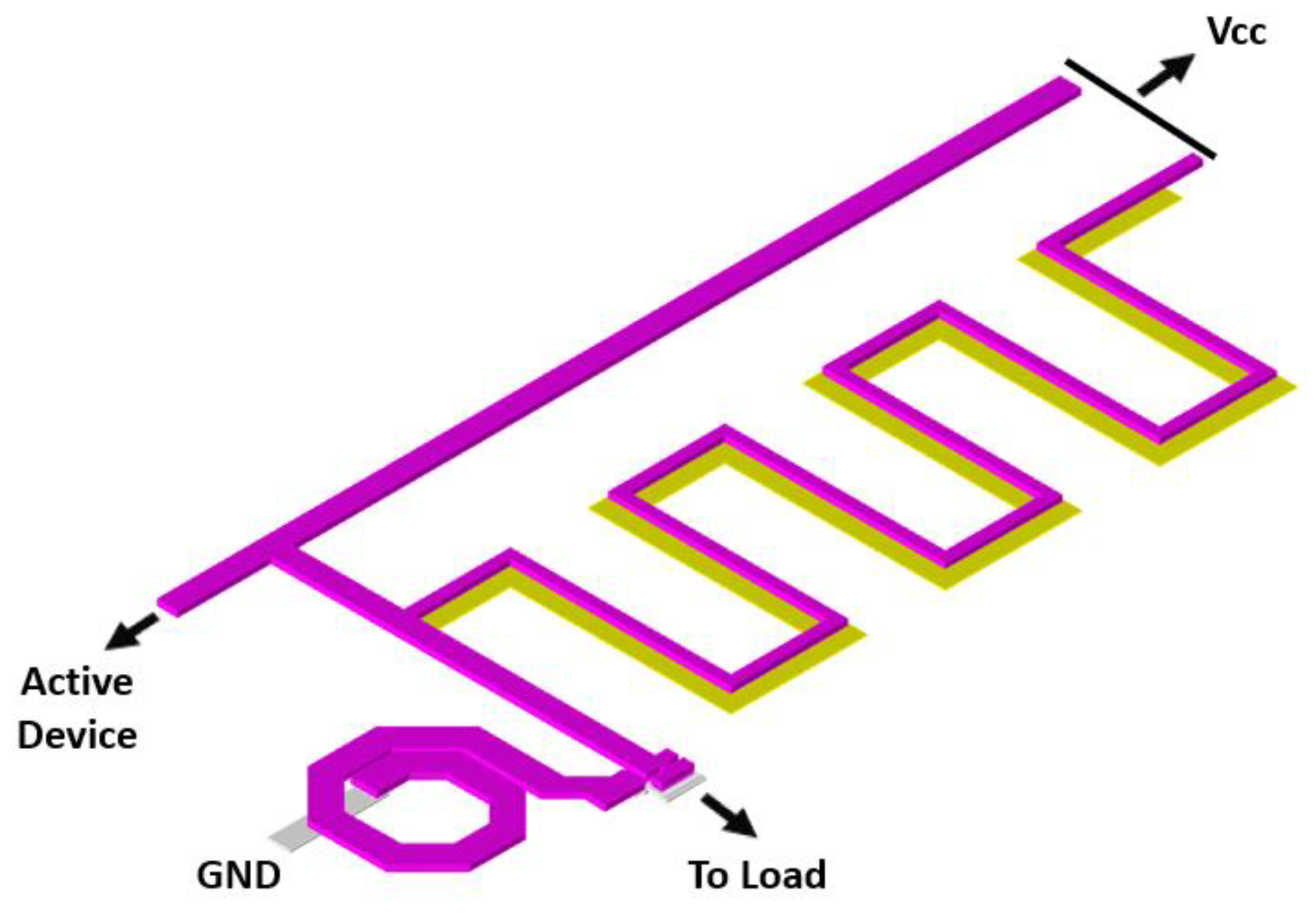
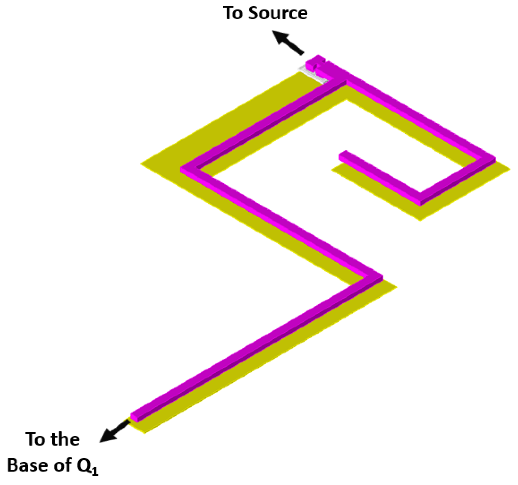
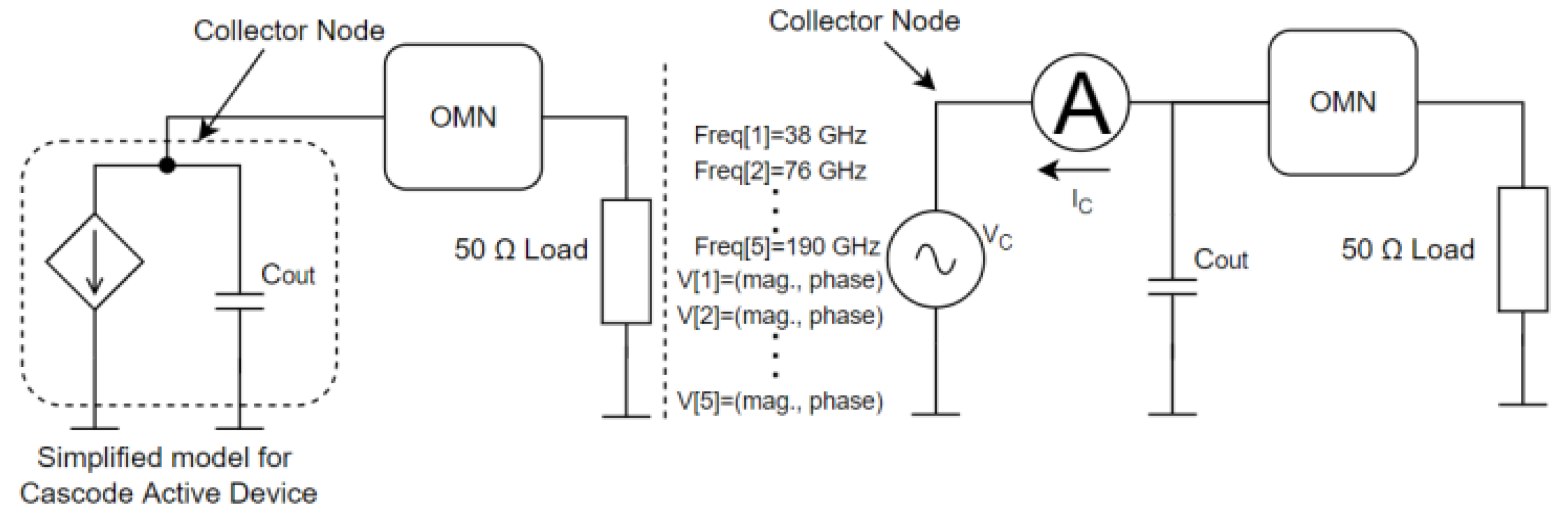
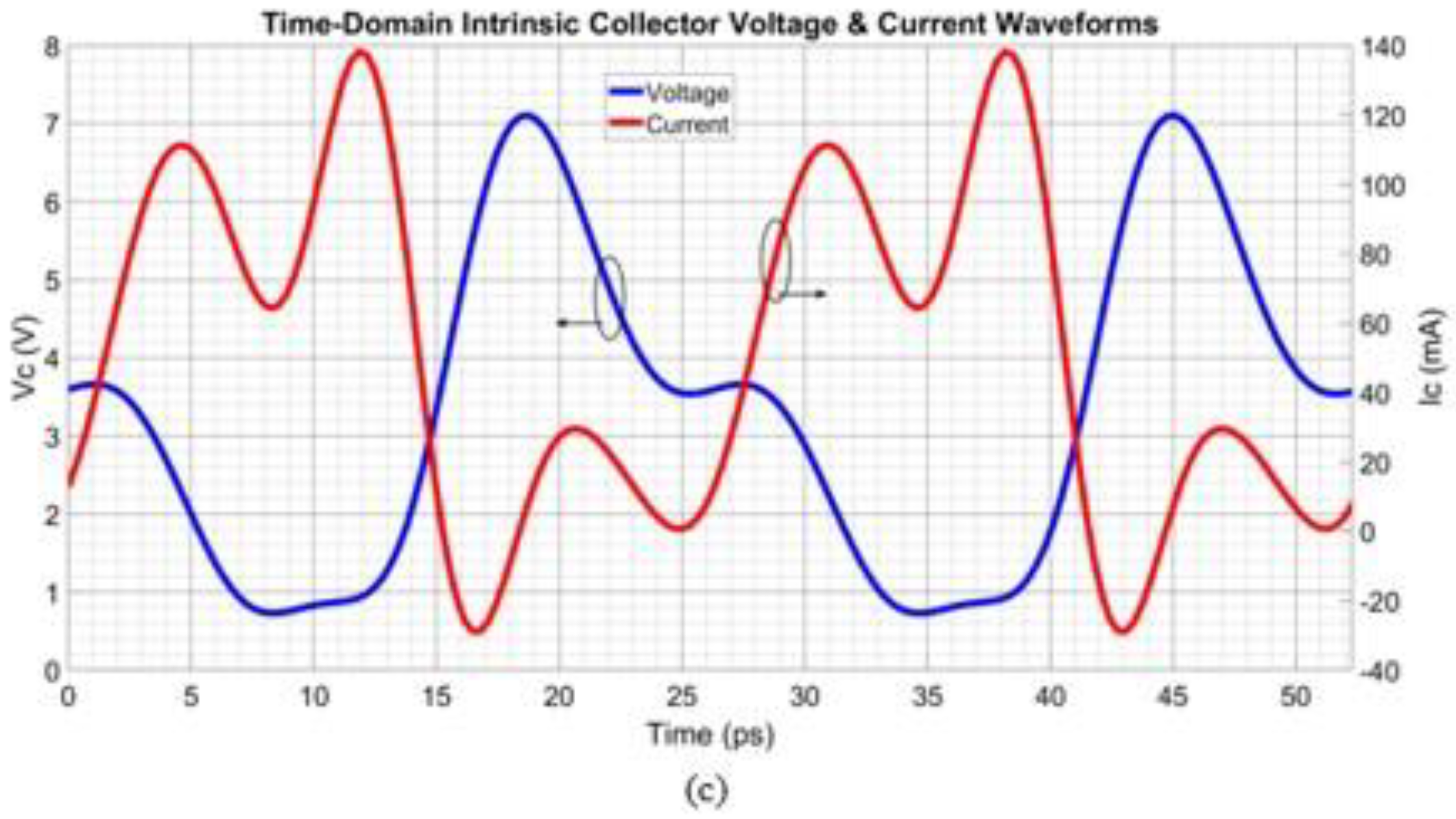
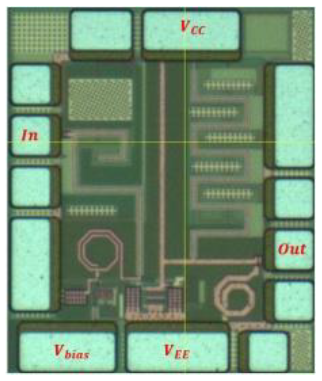
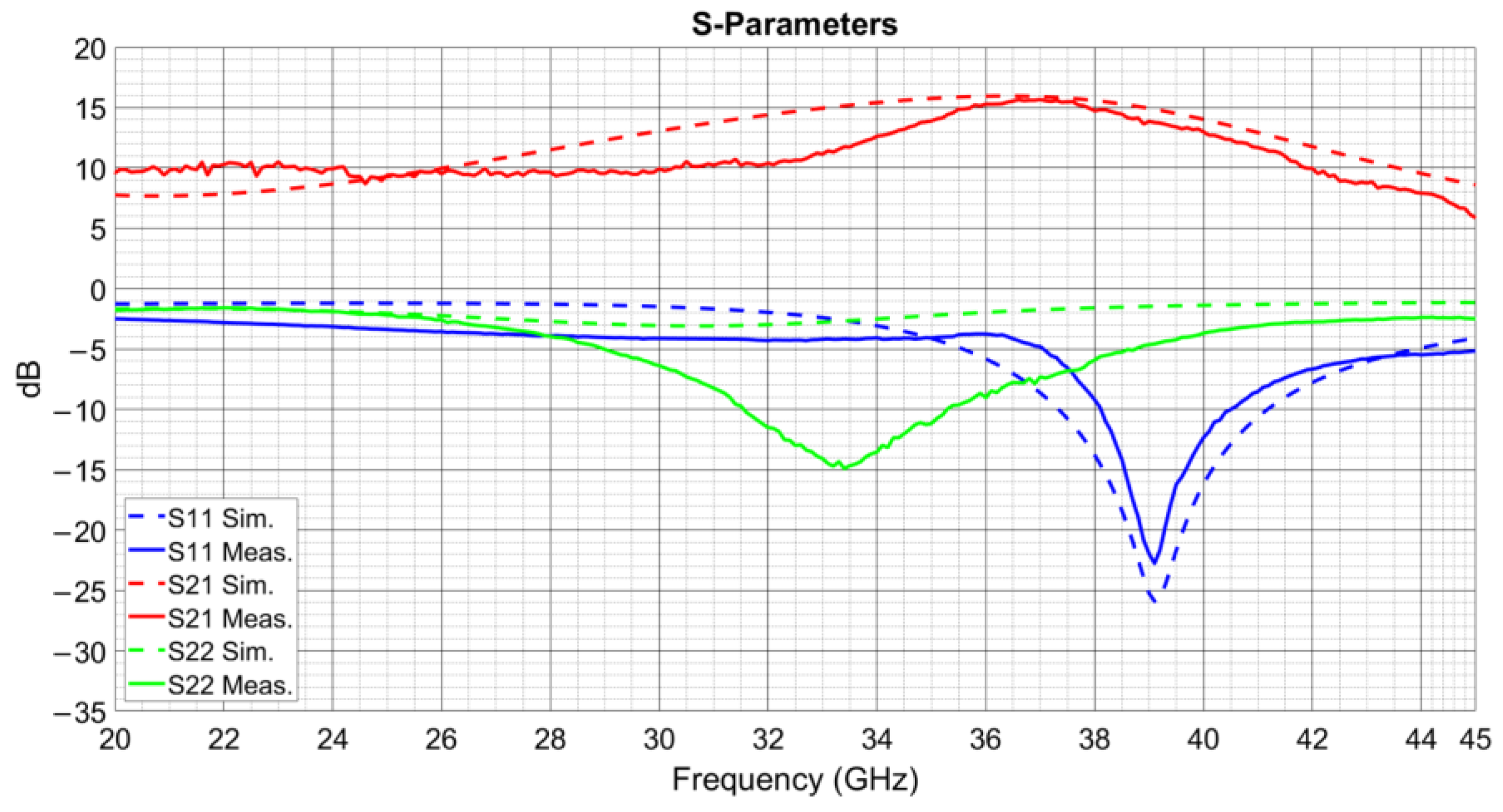
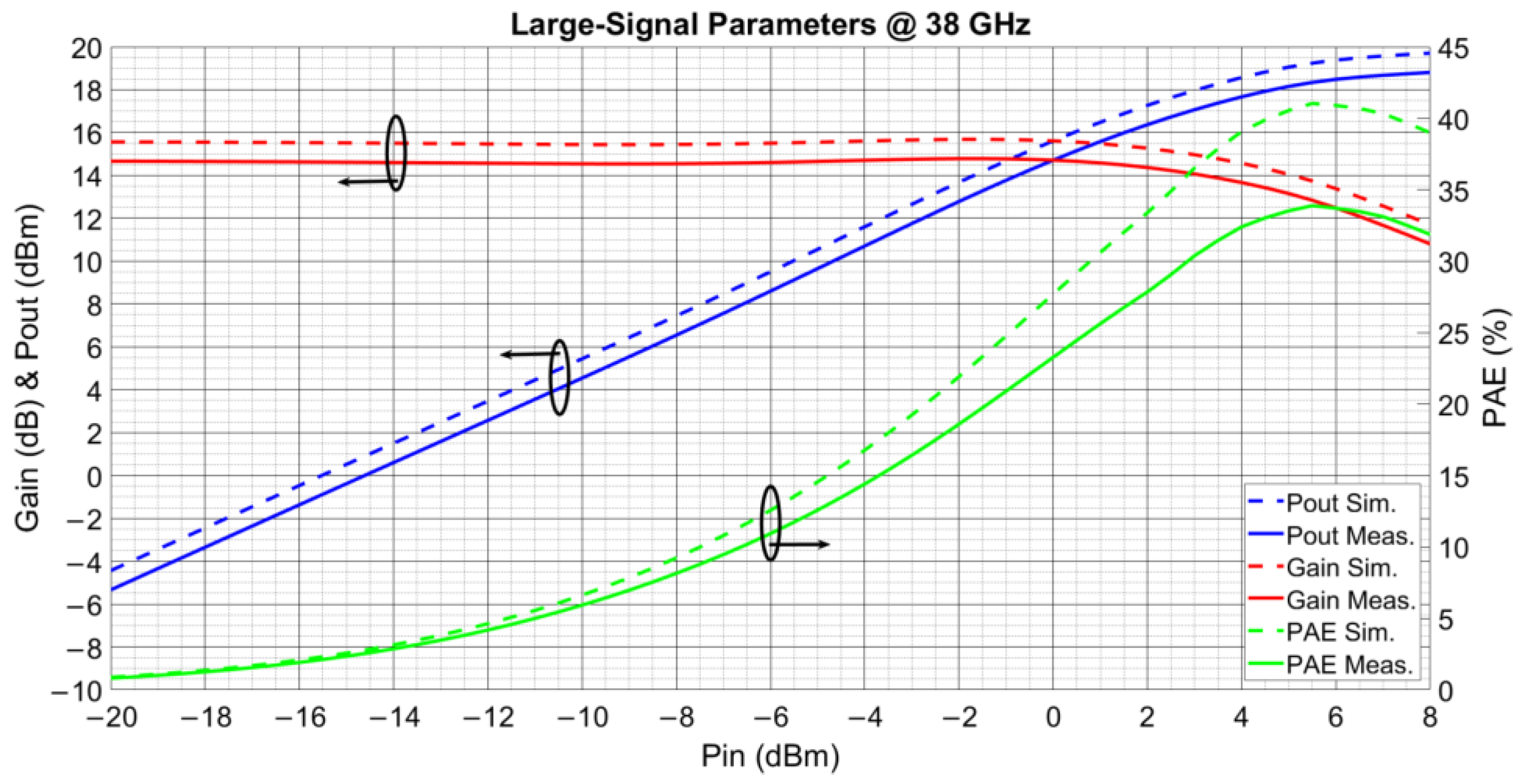
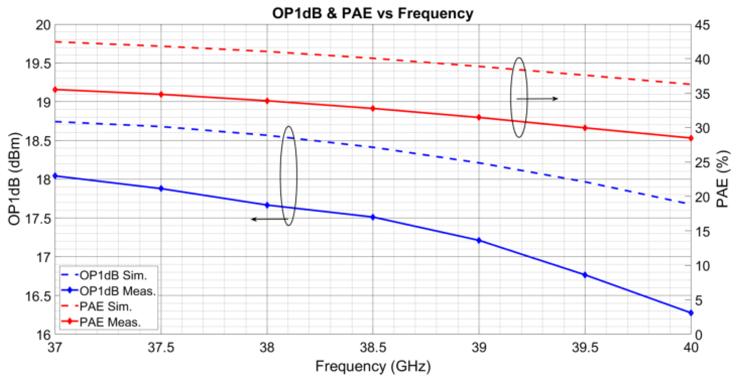
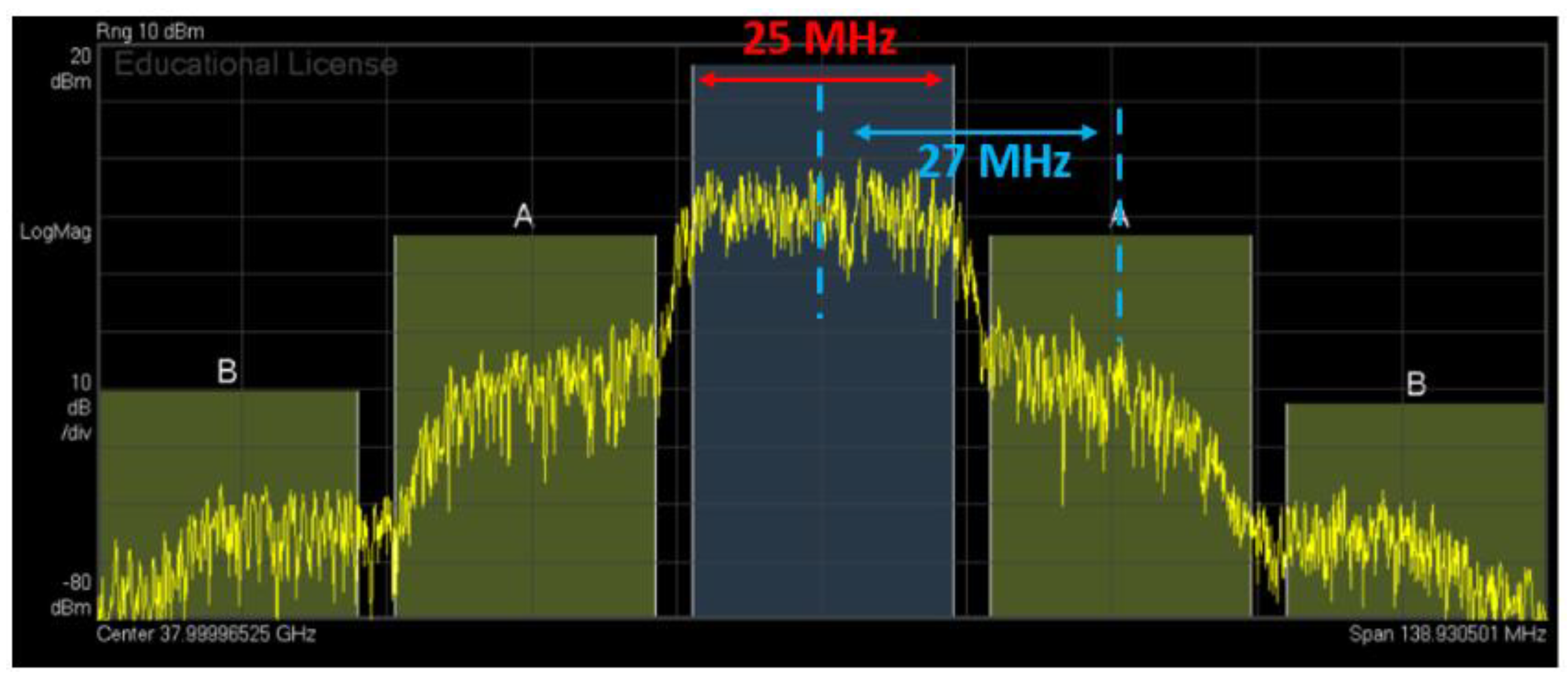
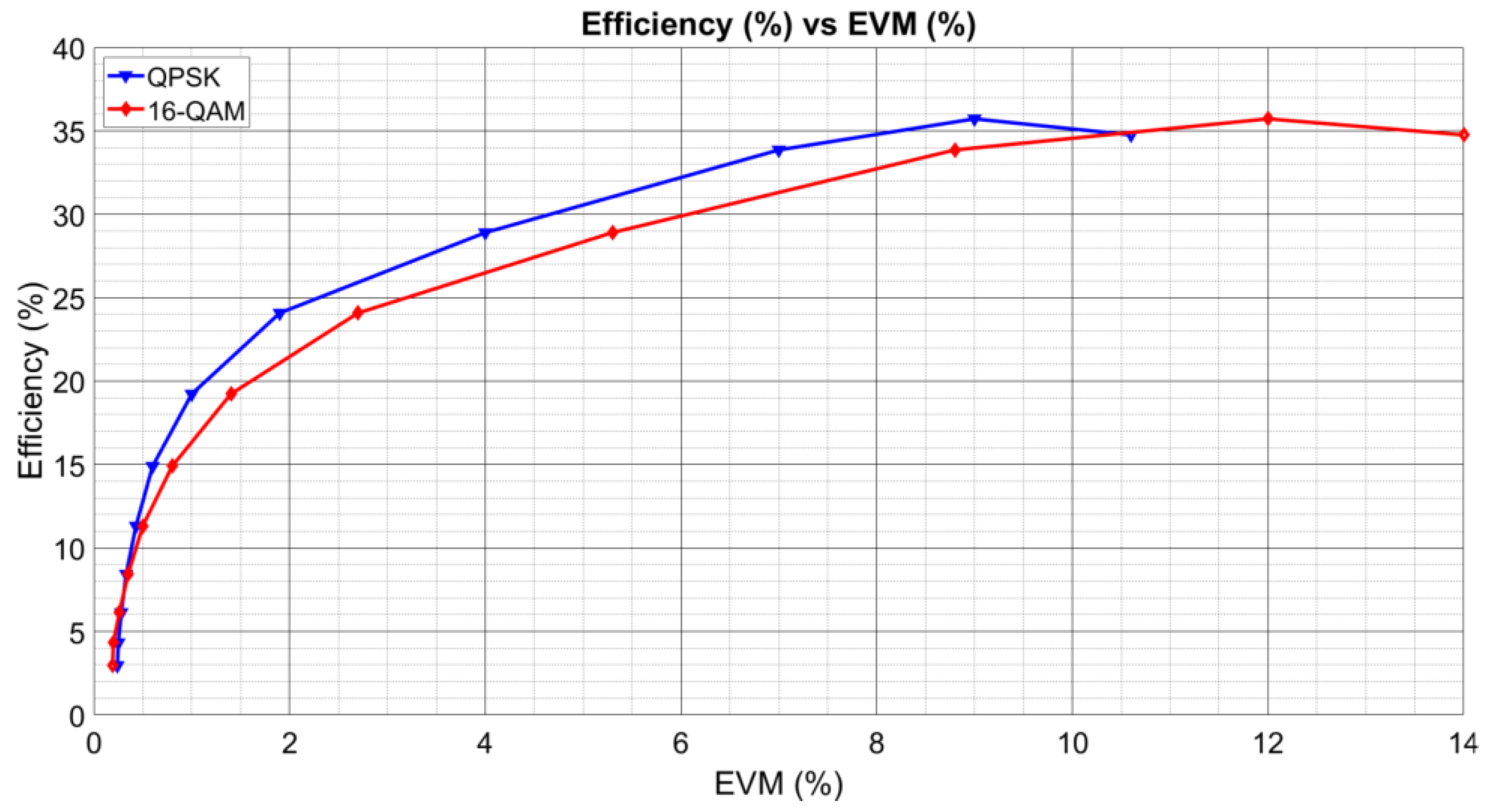
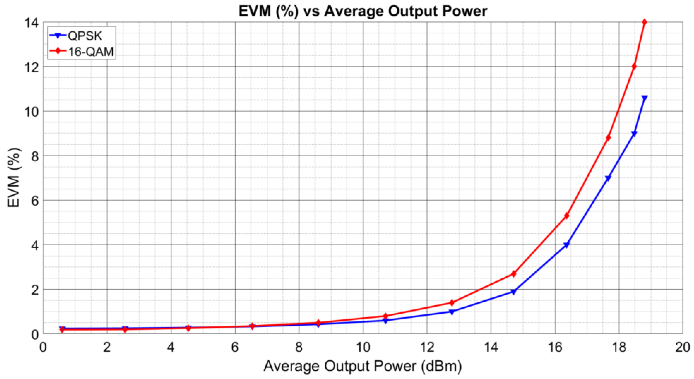
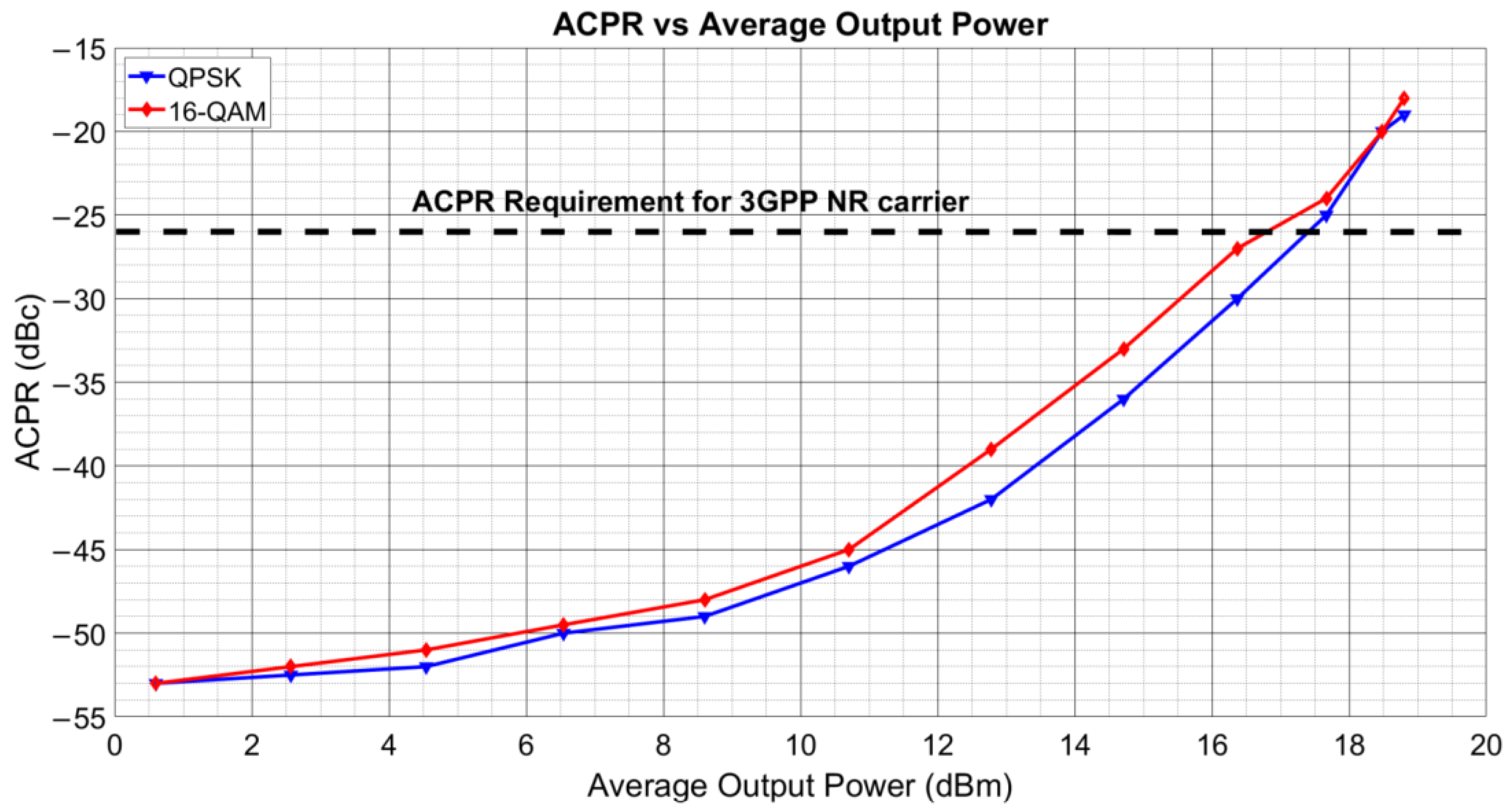
This paper deals with the design, analysis, and implementation of a Ka-band, single-stage, quasi-inverse class F power amplifier (PA). A detailed methodology for the evaluation of the active device’s output capacitance is described, enabling the designing of a second-harmonically tuned load and resulting in enhanced performance. A simplified model for the extraction of time-domain intrinsic voltage and current waveforms at the output of the main active core is introduced, enforcing the implementation process of the proposed quasi-inverse class F technique. The PA is fabricated in a 130 nm SiGe BiCMOS technology with fT/fmax=250/370 GHz and it is suitable for 5G applications. It achieves 33% peak power-added efficiency (PAE), 18.8 dBm saturation output power Psat, and 14.7 dB maximum large-signal power gain G at the operating frequency of 38 GHz. The PA’s response is also tested under a modulated-signal excitation and simulation results are denoted in this paper. The chip size is 0.605×0.712 mm2 including all pads.
Keywords: inverse class F; quasi-F−1; power amplifier; cascode amplifier; harmonic tuned PA; mm-wave PA; Ka-band PA; 37–40 GHz PA inverse class F; quasi-F−1; power amplifier; cascode amplifier; harmonic tuned PA; mm-wave PA; Ka-band PA; 37–40 GHz PA