Abstract
This paper presents a novel inductorless dual-mode buck-boost charge pump (CP) based DC-DC converter. The proposed architecture allows the same circuit to accomplish two modes of operation, buck and boost, for degrading or elevating the output voltage, respectively, compared to the input. To achieve each mode, only a switching of the input–output connections is needed without any other modification in the design of the DC-DC converter. The dual-mode configuration aims to merge two different functions into one circuit, minimizing the design time and the area the DC-DC converter occupies on the die. The proposed buck-boost CP has been designed using TSMC 65 nm complementary metal–oxide–semiconductor (CMOS) technology. The functional input voltage range of the CP in boost mode is 1.2 V to 1.8 V and the typical output voltage is 1.8 V. For the buck mode, the input voltage range is 3.2 V to 3.6 V and the output is 1.5 V. For both modes, the output can be easily modified to new values by changing the comparator configuration. Efficiency results are also provided for the two modes.
1. Introduction
In recent decades, the necessity for lower power consumption in the field of electronics has become crucial. Through this need, new technologies and techniques have been developed and a new era has emerged: the era of energy harvesting, which tries to eliminate the need for frequent battery recharge or replacement. Energy harvesting is the process in which ambient energy is collected from the environment, captured, and then converted into electricity to supply small autonomous devices. This is the reason why energy harvesting is often used in applications based on smart devices connected wirelessly, wearable devices, sensor networks [1], e.g., the Internet of Things (IoT), etc. Sometimes the energy that is harvested is not enough for the system to be functional and an extra power management system is needed. DC-DC converters have been developed to generate voltages for many applications to overcome this problem. Charge pumps, which are switched-capacitor topologies, are used in DC-DC converters, playing a major role in this process because they are simple to implement, can be fully integrated as they occupy a small chip area, and aim for a low-cost product. All these characteristics make CPs a suitable choice in low-power applications, replacing the linear voltage regulators (LDOs) that, in the past, formed a common solution in power conversion.
DC-DC converters can be categorized based on the employed means to make their charge transfer and voltage conversion. If they use inductors as energy storage elements, they are known as inductive DC-DC converters. Accordingly, if they use only capacitors to store and transfer charge, they belong in the category of switched-capacitor converters. Charge pumps belong to the second category as they consist of capacitors and switches. CPs transfer charge through capacitors to step up or step down the input-to-output voltage, usually with the aim of two non-overlapping and anti-phase clock signals. Inductorless CPs are a good option when power, area, and cost limitations are important. In contrast, inductive DC-DC converters use an external inductor to achieve the required inductance and, thus, they may have a higher driving capability, lower noise, and lower voltage ripple than switched-capacitor converters. However, overall, they are more expensive, area-consuming, bulky, and larger due to the cost and the size of the external inductor.
The operation of a DC-DC converter is to convert the input voltage to another voltage level at the output. Therefore, based on the voltage conversion, DC-DC converters are categorized into three types, buck, boost, and buck-boost. Buck converters step down the input voltage to a lower level at the output and boost converters step up the input voltage to a higher level at the output. Buck–boost converters combine the two modes with a single circuit, and they are very useful in systems that are battery-supplied because the charge of the battery gradually varies. With an overview of the literature, we can find different buck-boost topologies that have been developed over the years. A diode-based buck boost converter topology is depicted in Figure 1, which is an inverting buck-boost converter, meaning that the output voltage is of the opposite polarity to the input [2]. To overcome the opposite polarity problem, non-inverting topologies have been developed [3,4,5,6]. Many topologies implement both modes in one circuit [7] but they all use inductors and transformers, which increases the size and the cost of the converter.
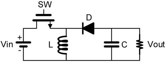
Figure 1.
Inverting buck-boost converter topology.
Accordingly, with a literature review of recent decades, many inductorless CPs can be found. For example, the Dickson CP is quite famous, mostly due to its simple design. The Dickson CP is an N-stage architecture consisting of switches and capacitors initially proposed and patented by J.F. Dickson [8] in 1976. Diode-connected transistors are used to transfer charge through the capacitors from stage to stage as shown in Figure 2. Each stage consists of a diode-connected transistor and a capacitor. The operation of this topology is based on the capacitors’ charging and discharging ability. In every clock period, the capacitor of each stage steps up and transfers its voltage to the next stage through the diode-connected transistors. In the Dickson CP architecture, the number of stages determines the final output voltage.

Figure 2.
N-stage basic Dickson CP.
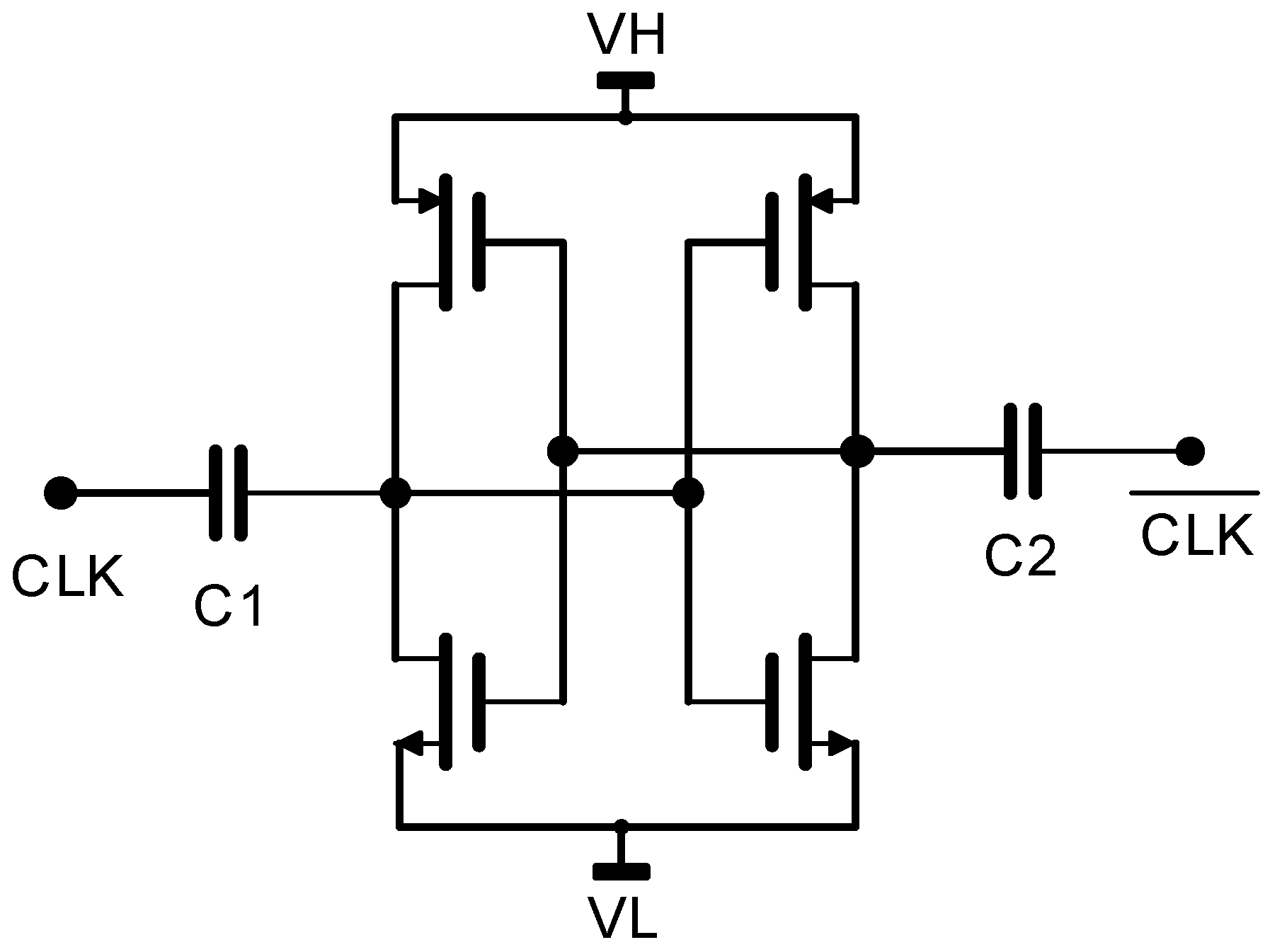
The main drawback of the Dickson topology is the mosfet threshold voltage drop, which causes low efficiency levels. Several other modifications of the Dickson CP topology have been proposed more recently, such as the charge transfer switch (CTS) CP, static and dynamic topologies [9,10], techniques such as the gate biasing [11,12] and the body biasing technique [13,14], and other variations. These topologies have been proposed mainly to overcome the mosfet threshold voltage drop problem. One modification was introduced by Favrat [15] and later used by Pelliconi [16] in a cascaded configuration. The topology is based on a cross-coupled inverter topology and it is shown in Figure 3.
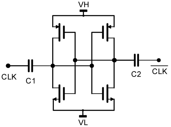
Figure 3.
Architecture of the cross-coupled CP.
In [17], an efficient inductorless buck-boost converter architecture is proposed, which is a switched capacitor topology based on the Favrat boost CP topology [15] that offers small number of transistors, reduced size, simple design, and high conversion efficiency levels. The Favrat topology is a voltage doubler that consists of two nmos and two pmos transistors and two flying capacitors driven by a two-phase clock (CLK and ). The proposed architecture in this paper expands the operating modes of the topology and it is proven that, with minor modifications, it can support the buck mode as well. The two modes, buck and boost, can be supported by the same core circuit, and a novel buck-boost converter is proposed without the use of any inductor. Each mode, buck or boost, is realized by switching only the external connections of the CP. In the current paper, a theoretical explanation for both operation modes is given. In [17], we presented the CP operation in boost mode receiving an input voltage of 2.2 V and converting it into a 3.3 V output voltage. Accordingly, in buck mode, with a 3.3 V input voltage, the CP gives a 1.6 V output voltage. In the present paper, the input voltage range of both modes is expanded and studied extensively in terms of efficiency under a wide range of input voltages and output current loads. More specifically, for the boost mode, the operating input voltage range is from 1.2 V to 1.8 V and the output voltage is 1.8 V. Accordingly, for the buck mode, the input voltage range is from 3.2 V to 3.6 V and the output is 1.5 V. The proposed architecture is designed in TSMC 65 nm CMOS technology. Furthermore, the details for the mode interchanging between buck and boost mode are described.
Therefore, in this paper, a novel CP is presented, which (a) is a dual-mode buck and boost within the same circuit, (b) is inductorless, and (c) at the same time, presents high efficiency. The sections of the present paper are organized as follows: in Section 2, the proposed buck-boost DC-DC converter architecture is described, and the individual blocks of the design are analyzed in detail. In Section 3, the proposed dual-mode DC-DC converter postlayout simulation results are presented in each operating mode, in Section 4, the efficiency results are presented for both modes, and finally, in Section 5, the conclusions of this work are given.
2. Circuit Architecture
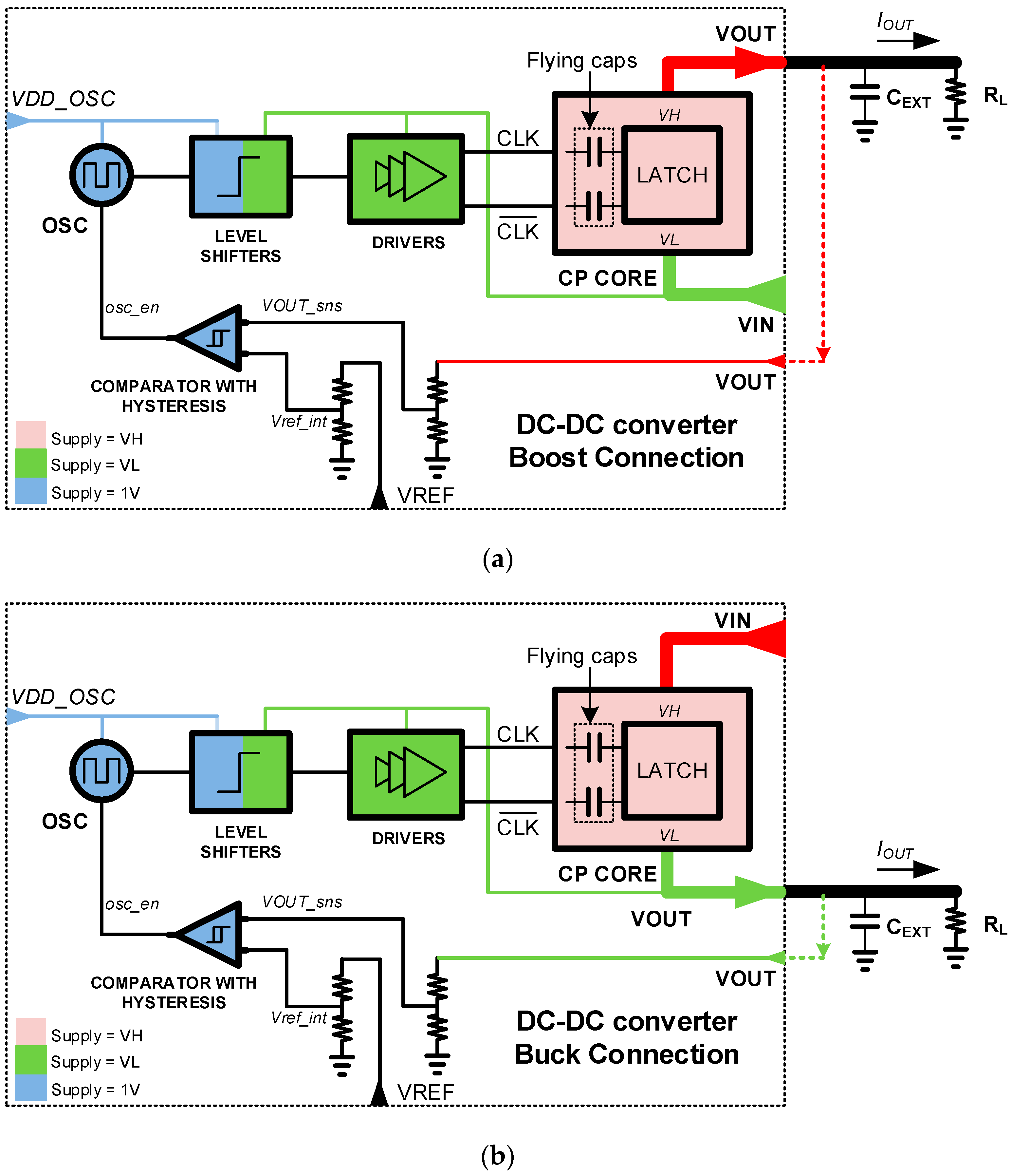
The proposed top-level architecture of the buck-boost DC-DC converter is shown in Figure 4. The converter consists of an oscillator (OSC) with a 35 MHz operating frequency, a level shifter, a comparator, a suitable number of pre-drivers and drivers, and finally, the core of the CP.

Figure 4.
Proposed buck-boost DC-DC converter: (a) boost mode connection and (b) buck mode connection.
The core of the CP is a latch consisting of two inverters connected in a cross-coupled topology, as shown in Figure 3. The core also consists of two pumping capacitors that are connected to the latch, and their value is equal to 210 pF each. The size of the pumping capacitors is related to the switching frequency and decreases as the switching frequency increases, thus reducing the area the CP occupies and improving the power efficiency simultaneously. However, high frequency levels increase the losses due to parasitic elements. Therefore, the value of the flying capacitors has to be chosen considering design issues such as the area, the frequency, and the power losses due to parasitic elements. The initial size of the flying capacitors can be determined from the desired output current and the switching frequency using Equation (1):
However, in practice, as the efficiency of the CP can be affected by the size of the pumping capacitors, their final value is determined through simulations. The power consumption of the oscillator, the level shifter, the drivers, and the comparator can also affect the efficiency of the CP. Of these, the drivers are the most important factor in the efficiency degradation, as they must be high enough to drive the core of the CP.
Apart from the input voltage (VIN) and the output voltage (VOUT) of the CP core, one supply voltage (VDD_OSC) is needed to power the oscillator. This voltage is provided externally of the CP and usually is available from the overall system in which the DC is incorporated. This supply must always be available to the oscillator for the CP to be able to start operating when required. The oscillator supply voltage is equal to the technology core transistors’ operating voltage and in our case is 1 V. The same voltage also supplies the other supporting parts of the circuit, which are the comparator and partially the level shifter. The supply voltage of the core is in the range of 1.2 V to 1.8 V for the boost mode and from 3.2 to 3.6 V for the buck mode.
2.1. Oscillator
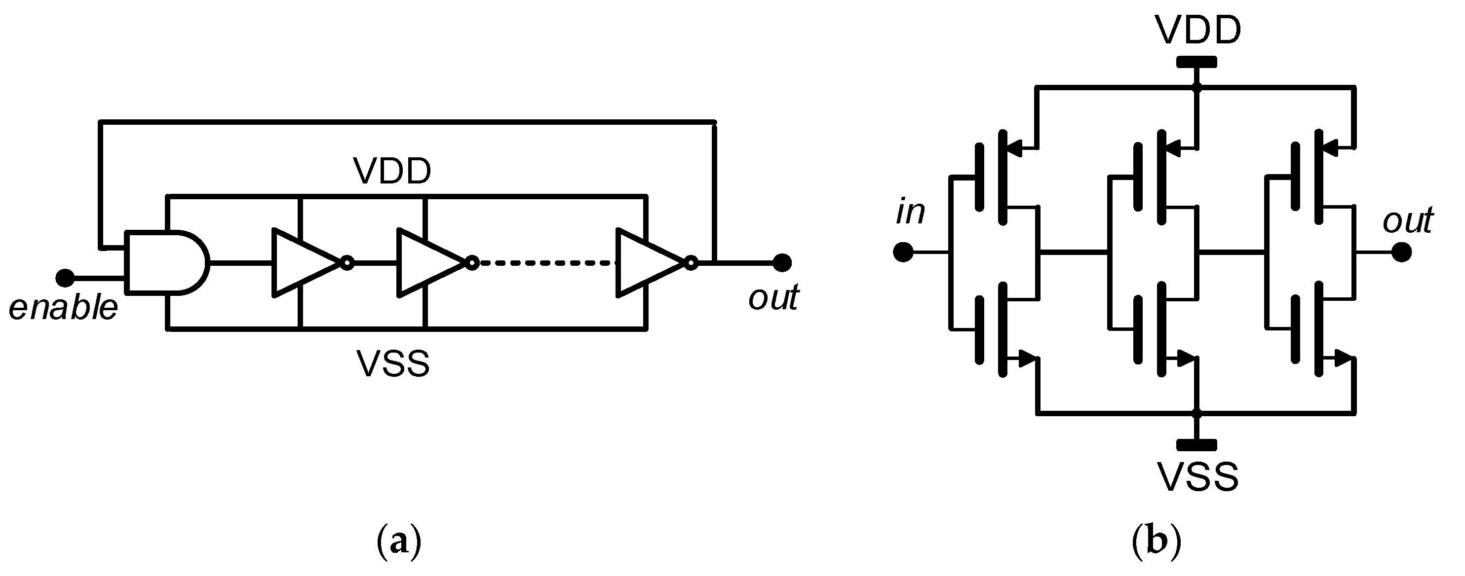
The switches of the core need a clock signal for their operation, so a conventional ring oscillator suitable to produce the required clock has been employed. The topology of the ring oscillator is shown in Figure 5, and it consists of an adequate number of delay cells in a closed loop. Each delay cell of the ring oscillator has three inverters connected in series, forming an inverter chain. The clock frequency of the oscillator is determined by the number of inverters inside the delay cells. The number of employed delay cells in combination with the number of inverters inside of them adjusts the oscillator frequency. The ring oscillator topology that has been selected has a simple design and offers a wide tuning range and low power consumption.

Figure 5.
Oscillator architecture: (a) block diagram of the oscillator and (b) the delay cell.
For this application, the oscillator performance and its operating frequency are not crucial and, therefore, the oscillator of the circuit operates as a free-running oscillator. The switching frequency of the proposed CP has been selected at 35 MHz with a supply voltage of 1 V. Without using any other capacitors or inductors, the topology is ideal for low-power applications with a small layout area.
2.2. Comparator
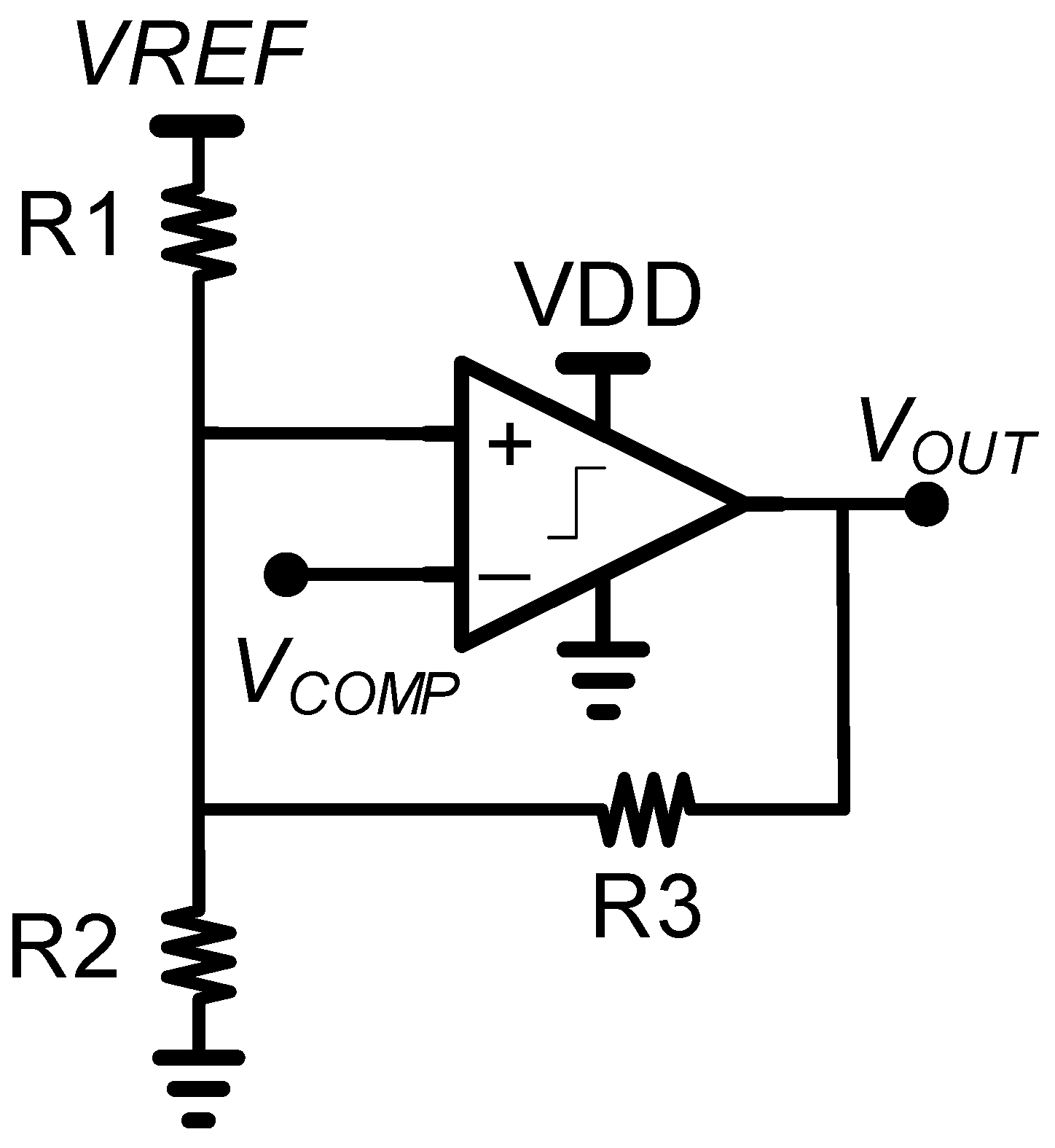
A comparator with hysteresis, as shown in Figure 6, is used for comparing the CP output voltage with the thresholds (maximum and minimum levels) of the required output voltage. The oscillator is activated by the comparator when the output voltage is lower than the minimum threshold to start the charging process. The oscillator is deactivated by the comparator when the maximum voltage is achieved. The consumption of the load at the output is responsible for the gradual discharge of the output until the lower threshold, where the charging starts over. The comparator with hysteresis has been used to switch properly between the two thresholds and to be insensitive to other voltage noise and ripple. For the comparison, an external reference voltage coming from a constant voltage reference is required. VCOMP is the scaled voltage coming from the CP output voltage VOUT.

Figure 6.
The comparator with hysteresis topology.
2.3. Level Shifter and Driver
From Figure 4, it can be seen that the proposed DC-DC converter requires level shifters to convert the oscillator output switching voltage to the voltage level needed in the switches of the CP core. Level shifters operate by using two supply voltages, the input supply voltage, which should be the same as the oscillator supply voltage, and the output supply voltage coming from the lower voltage of the CP core (VL), which depends on the operating mode and is either the input (VIN) or the output (VOUT) voltage. Thus, the driving voltage of the level shifter transistors is always at the correct level. In more detail, for the operation of the boost mode, the level shifter input supply voltage is 1 V, which is the oscillator supply voltage, and the output supply voltage is the same as the input supply voltage of the core of the CP (VIN). When the buck mode is selected, the level shifter input supply voltage is equal to the oscillator supply voltage again, but now the output supply terminal is connected to the output of the CP, so the clock has the required amplitude. Drivers need to drive the core of the CP properly and so their supply voltages have to be at the same level as the output supply voltage of the level shifter. In addition, for the correct operation of the level shifter, the external capacitor at the output of the circuit must be pre-charged to some voltage level. Otherwise, the system would not be able to work. This is not required for the boost mode operation.
2.4. Core of the Charge Pump
The operation of the CP core in boost mode, which is based on Favrat architecture, is depicted in Figure 7, and the operation of the topology is as follows: assuming the first semi period as phase 1, the complimentary clock signals CLK and are low and high, respectively, so in phase 1, transistor M1 is on and M3 is off and capacitor C1 is charged to VIN. At the same time, C2, which has already been charged in VIN, now charges the capacitor of the output, the voltage of which scales up to 2 × VIN through M4, which is on. During phase 2, which is the second semi period, CLK is high and is low and the operation of the pumping capacitors is reversed, respectively. Therefore, in phase 2, M2 is on and M4 is off and capacitor C2 is charged to VIN. At the same time, C1 charges the output capacitor through M3, which is now on, to 2 × VIN. The procedure of the charging of the flying capacitor and the discharging on the output capacitor in each semi period is depicted in Figure 7a. The operation of the core in the boost mode is shown in Figure 7b. The output voltage for boost mode is given by the expression
VOUT = VIN + VCFLY = 2 VIN

Figure 7.
Boost cross-coupled CP (a) charge/discharge and (b) core of CP in boost mode.
Accordingly, the operation of the buck mode is depicted in Figure 8. In phase 1, CLK is high and is low, so M3 is on and capacitor C1 is charged to VIN−VOUT. At the same time, C2 discharges through M2, which is on, on the output capacitor, the voltage of which is now equal to VIN/2. During phase 2, CLK is low and is high and the operation of the pumping capacitors is reversed, respectively. Now, transistor M4 is on and the flying capacitor C2 is charged to VIN−VOUT. Simultaneously, capacitor C1 discharges through M1, which now is on, on the output capacitor. The charging of each of the flying capacitors in each semi period and the discharging on the output capacitor can be seen in Figure 8a. The operation of the core in the buck mode is shown in Figure 8b. Equations (3) and (4) represent the charging and discharging phase of the buck mode.
VCFLY = VIN − VOUT
VOUT = VIN/2

Figure 8.
Buck cross-coupled CP (a) charge/discharge and (b) core of CP in buck mode.
3. Proposed Buck-Boost CP Operation and Verification
The proposed buck-boost CP is able to operate in two modes, buck and boost, and it was designed and simulated in TSMC 65 nm technology. All the presented results are based on postlayout simulations. The system can operate in each of the two modes, only by interchanging the output (VOUT) and input (VIN) between the low voltage (VL) and the high voltage (VH) terminals of the CP as depicted in Figure 9. More specifically, for the boost mode operation, the voltage of the input is connected to the VL terminal and the output of the CP is connected to the VH terminal. In buck mode, the input is connected to the VH terminal and the output is connected to the VL terminal. Additionally, the resistors of the comparator, which define the internal voltages for the comparison, must be reconfigured between the two modes. However, these resistors can also be reconfigured to readjust the output voltage level if it is required, but this is not applied in our case.
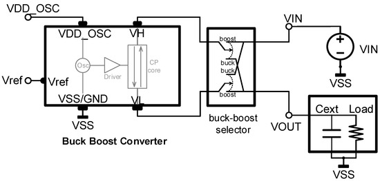
Figure 9.
External connectivity for switching between boost and buck mode.
The implementation of the buck-boost selector that is responsible for controlling the desirable mode selection is depicted in Figure 10. The desirable mode is selected by the SL terminal, which is connected to VSS for the boost mode and is connected to VIN for the buck mode.
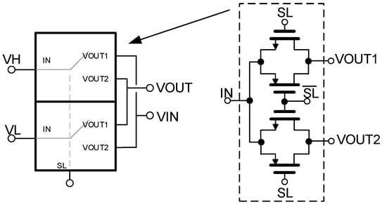
Figure 10.
The architecture of the buck-boost selector.
3.1. Boost Mode Simulation Results
The CP core operation is demonstrated in the time domain in Figure 11a,b, presenting the current waveforms through the flying capacitors and the mos transistors, corresponding to the operation described in Section 2.4 and Figure 7a,b. In Figure 11a, the current waveforms are depicted from the left side of the core CP including the capacitor C1 and transistors M1 and M3, and in Figure 11b, the current waveforms are depicted from the right side of the core CP including the capacitor C2 and transistors M2 and M4. In phase 1, the capacitor C1 is charged through M1, which is on, while M3 is off, and C2 pumps its charge to the output through the activated transistor M4, while M2 is off. In phase 2, the capacitor C1 pumps its charge to the output through the activated transistor M3, while M1 is off, and C2 is charged through M2, which is on, while M4 is off. The non-switching operation, observed at the beginning and at the end of the waveforms in Figure 11a,b corresponds to the time that the output voltage VOUT has reached its maximum threshold and the comparator set the oscillator off to make the CP stop charging.

Figure 11.
Current waveforms of the flying capacitors C1 and C2 and the core devices (a) M1 and M3 and (b) M2 and M4 in boost mode.
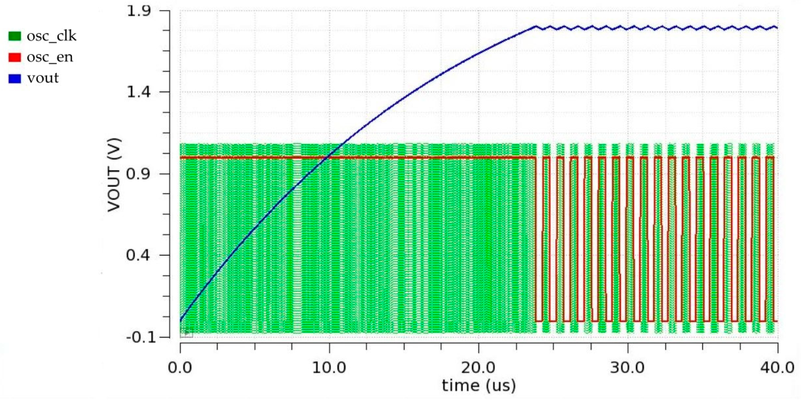
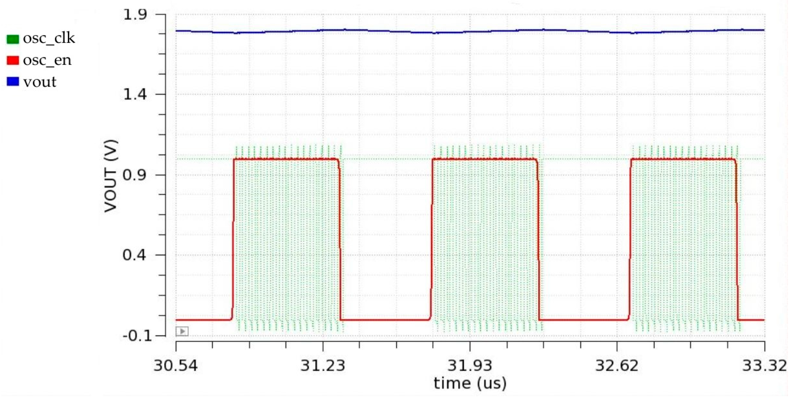
The postlayout simulation results of the boost mode in transient operation are presented in Figure 12. The plot shows the output voltage of the CP, oscillator output, and the enable signal, including the start-up time. Additionally, these results are shown for a better view within a short time in Figure 13, where the CP has reached the final voltage and has been set in normal operation. For these simulation results, the voltage of the input is 1.3 V, the output voltage is 1.8 V, and a load current equal to 5 mA is connected to the output of the CP.

Figure 12.
Postlayout simulation results in boost mode. DC output voltage with enabling signal and oscillator output (VIN = 1.3 V, VOUT = 1.8 V, Cext = 100 nF).
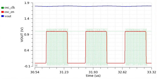
Figure 13.
Postlayout simulation results in boost mode. DC output voltage with enabling signal and oscillator output. Closer view during oscillator activation (VIN = 1.3 V, VOUT = 1.8 V, Cext = 100 nF).
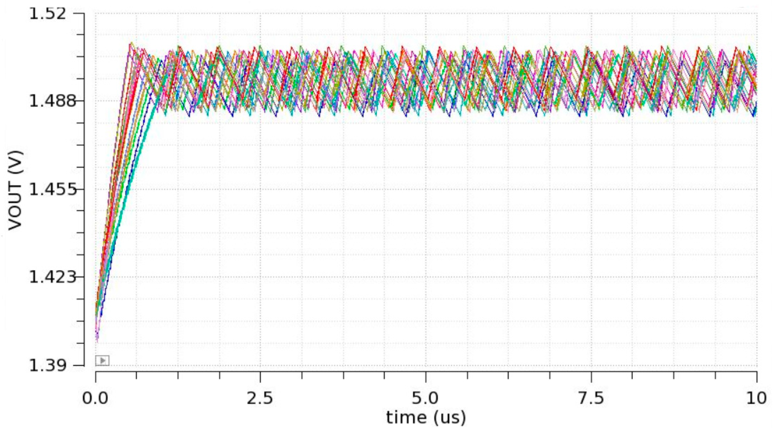
As shown in Figure 12 and Figure 13, the converter starts operating, the oscillator is enabled, and the CP charges the external capacitor, which is equal to 100 nF, with the load that is connected to the output. When the output becomes equal to 1.8 V, the comparator disables the oscillator and the circuits enter the steady state. The comparator reactivates the oscillator and the charging procedure starts over again every time the output voltage is lower than the minimum threshold. Additionally, the PVT corner simulation results are shown in Figure 14 across a temperature range from −40 °C to 125 °C including typical, fast, and slow corners, which verifies the robustness of the proposed circuit in boost mode.
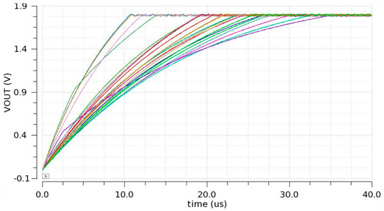
Figure 14.
PVT corners postlayout simulation results in boost mode (VIN = 1.3 V, VOUT = 1.8 V, Cext = 100 nF).
3.2. Buck Mode Simulation Results
Figure 15a,b presents the current waveforms through the flying capacitors and the mos transistor of the CP core in the time domain of the buck mode, in correspondence with the operation described in Section 2.4 and Figure 8a,b. In Figure 15a, the current waveforms are depicted from the left side of the core CP including the capacitor C1 and transistors M1 and M3, and in Figure 15b, the current waveforms are depicted from the right side of the core CP including the capacitor C2 and transistors M2 and M4. In phase 1, the capacitor C1 is charged through M3, which is on, while M1 is off, and C2 pumps its charge to the output through the activated transistor M2, while M4 is off. In phase 2, the capacitor C1 pumps its charge to the output through the activated transistor M1, while M3 is off, and C2 is charged through M4, which is on, while M2 is off. The non-switching operation, observed at the beginning and at the end of the waveforms in Figure 15a,b corresponds to the time that the output voltage VOUT has reached its maximum threshold and the comparator set the oscillator off to make the CP stop charging.

Figure 15.
Current waveforms of the flying capacitors C1 and C2 and the core devices (a) M1 and M3 and (b) M2 and M4 in buck mode.
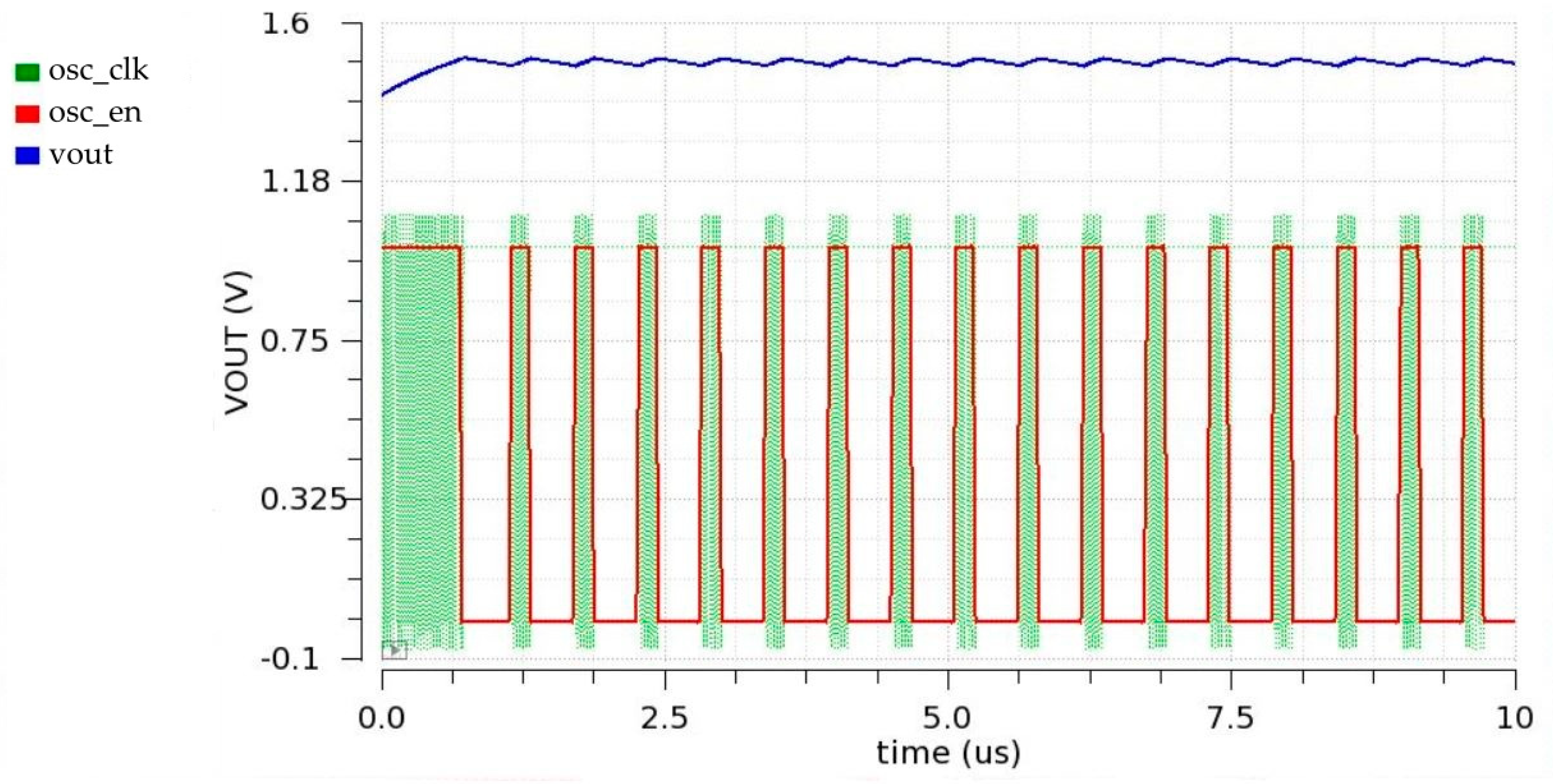
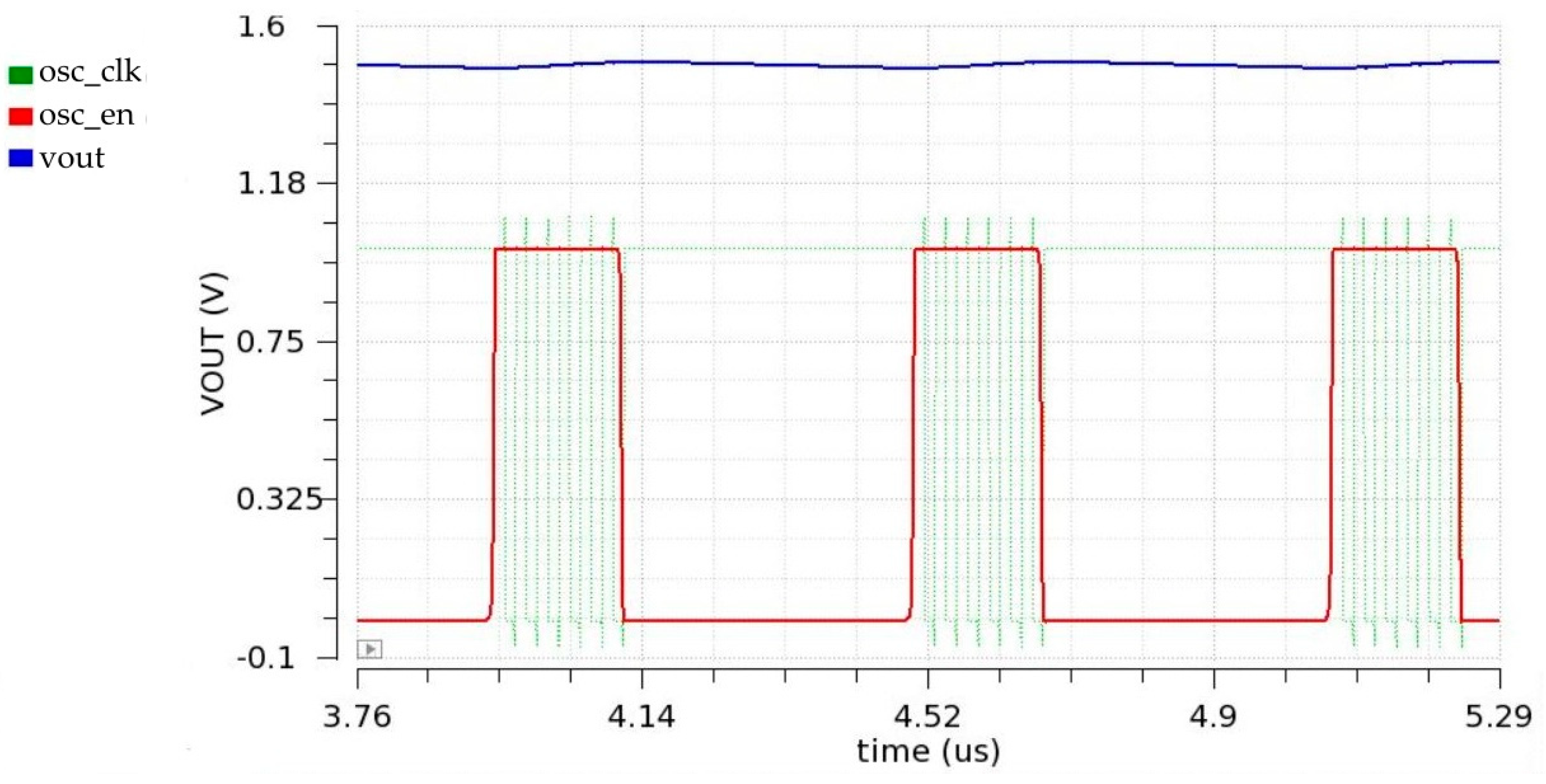
The buck mode postlayout simulation results are presented proportionally to those of the boost mode in Figure 16 and Figure 17. The input voltage of the buck mode is 3.4 V and the output is 1.5 V. The capacitor of the output in the buck mode must be precharged for the system to be able to start operating correctly and to step down the voltage of the input to the desired voltage level at the output. The precharging is needed to set the minimum required voltage for the transistors inside the latch and to help them to get out of the cutoff region. The output capacitor is 100 nF, and a 5 mA load is also connected to the output of the CP.
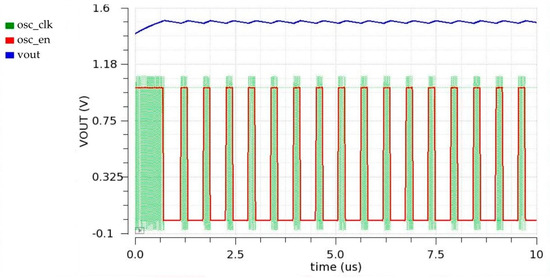
Figure 16.
Postlayout simulation results in buck mode. DC output voltage with enabling signal and oscillator output (VIN = 3.4 V, VOUT = 1.5 V, Cext = 100 nF).

Figure 17.
Postlayout simulation results in buck mode. DC output voltage with enabling signal and oscillator output. Closer view during oscillator activation (VIN = 3.4 V, VOUT = 1.5 V, Cext = 100 nF).
In Figure 18, the corner simulation results over PVT are depicted for the buck mode of the CP, and similarly to the boost mode, the corner simulation results include typical, fast, and slow corners across a temperature range from −40 °C to 125 °C.
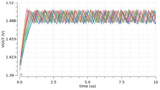
Figure 18.
PVT corners postlayout simulation results in buck mode (VIN = 3.4 V, VOUT = 1.5 V, Cext = 100 nF).
4. Efficiency Results
Power efficiency may be the most crucial parameter in the CP design [18]. The power efficiency of a CP is affected by several factors such as the switching frequency of the oscillator, the size of the flying capacitors, and the driver strength. Reasons that are responsible for low power efficiency levels are power losses due to clocks’ signals overlapping and parasitic capacitances of the switching devices [19]. Higher efficiency levels can be achieved by reducing the area that the CP occupies. However, there is a tradeoff between the clock frequency, the size of the switches, and the size of the flying capacitors to achieve optimum efficiency results. Overall, higher switching frequencies allow smaller sizes for the flying capacitors.
Ideal CPs have no parasitic capacitances and the threshold voltage drop of the switching devices is zero [20]. However, in real CPs, there are losses due to parasitic elements, switch threshold voltage drop, parasitic capacitances of the top and bottom plates of the flying capacitors, and losses that stem from the operation of all the subcircuits of the CP such as the oscillator, the level shifter, the comparator, and the clock drivers. The operation of these additional circuits reduces the efficiency of the CP considerably. Additionally, the switching devices of the CP cause energy losses due to the charging and discharging of their internal capacitances and inductances, and these losses are becoming worse for higher switching frequencies [21]. The power efficiency of a non-ideal switched capacitor converter can also be affected by the output load conditions. A converter that can drive heavy loads needs different design parameters than a converter that is able to drive lighter loads, so under different load conditions, the converter may not maintain its high power efficiency levels, and as a result, its parameter designs have to be adjusted to the load [22].
The expression of power efficiency for a switched capacitor converter is
where VIN is the input voltage of the CP, IIN is the input current, and, accordingly, VOUT is the output voltage and IOUT is the output current of the converter. IIN is the total current that the core and the additional circuits consume.
The core of our proposed architecture is a voltage doubler and so the input average current is expected to be almost twice the output average current [23]. This can be derived from the equation
where N is the number of the CP stages, which in our case is 1, α is a factor that is equal to the parasitic capacitance of the bottom plate over the flying capacitors’ value, and IL is the current of the load at the output [24]. Therefore, based on Equations (5) and (6), the theoretical efficiency of the CP, assuming an ideal CP with zero losses (α = 0), is
To estimate the simulation efficiency of a switched capacitor converter, we need to measure the input and the output current during the steady state when the output capacitor is fully charged to the desired output voltage level with the output load connected. To calculate the simulation efficiency, we use Equation (5).
4.1. Boost Mode Efficiency Results
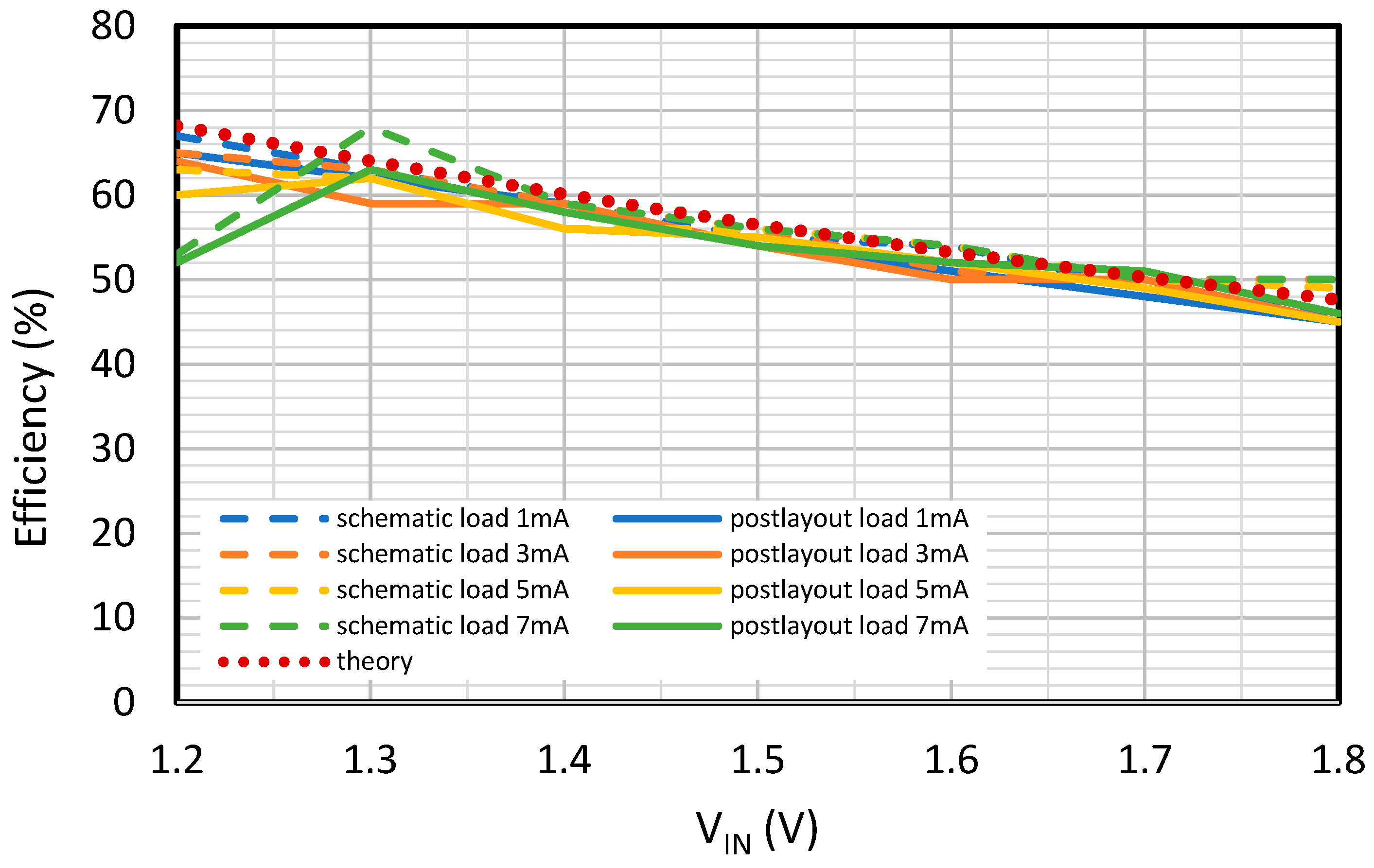
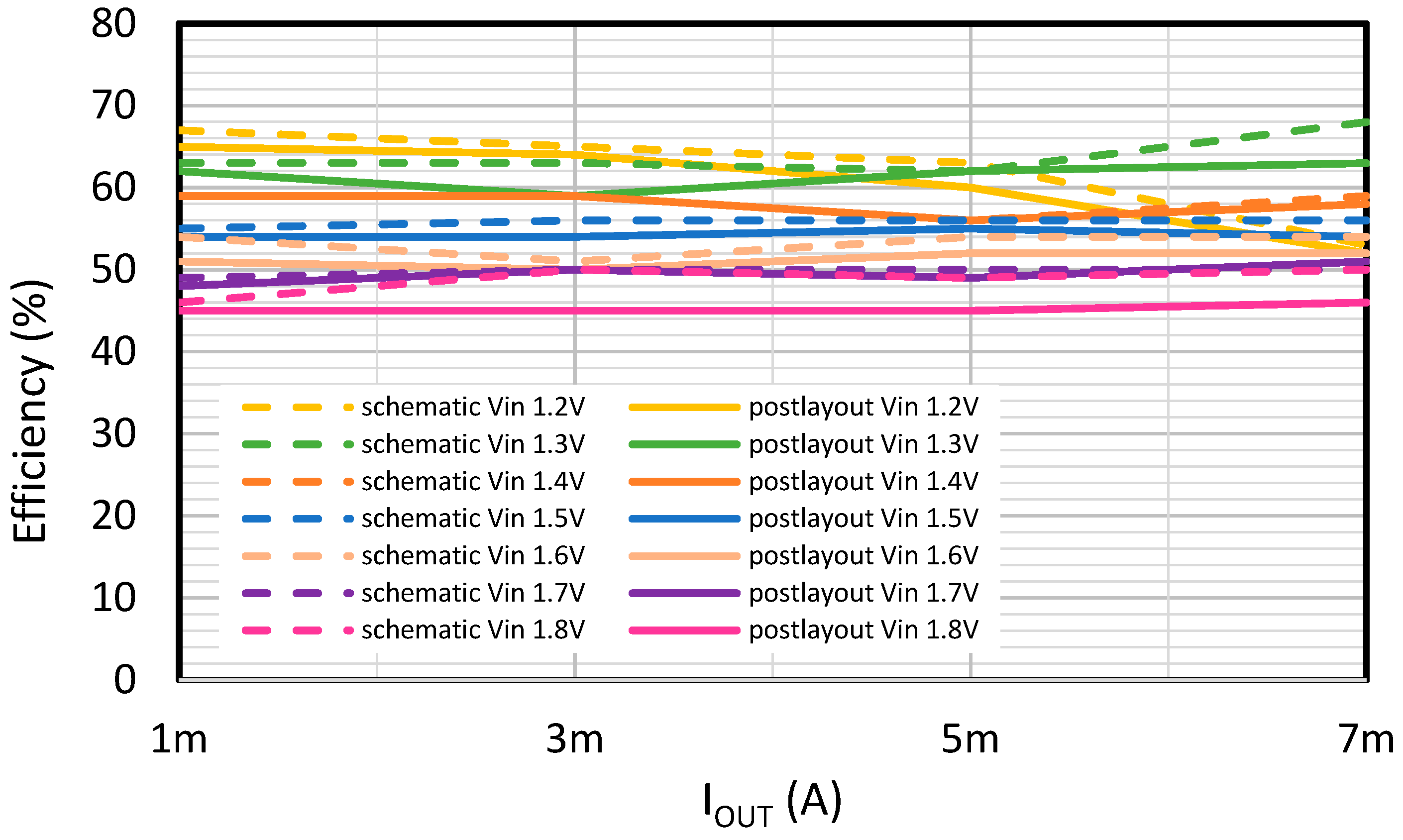
In Figure 19, efficiency levels for the boost mode can be seen for several input voltages from 1.2 V to 1.8 V. The output voltage is fixed at 1.8 V. In Figure 19, we can notice that for input voltages between 1.2 V and 1.8 V, the simulation efficiency results are close to the expected values of the theory. Additionally, it is noticeable that the optimum operating point where the power efficiency is maximized seems to be when the input voltage is equal to 1.3 V. In addition, Figure 20 depicts the efficiency of the boost mode over different output load currents and for different input voltages.
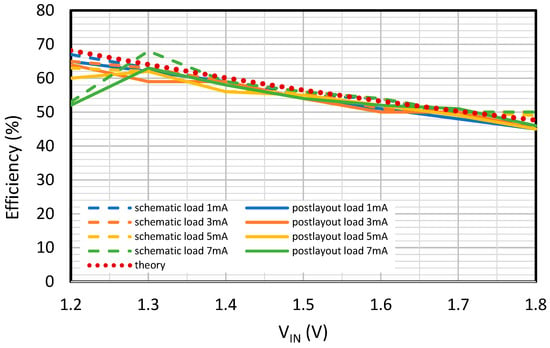
Figure 19.
Efficiency vs. input voltage for the boost mode (VOUT = 1.8 V).

Figure 20.
Efficiency vs. load current for the boost mode (VOUT = 1.8 V).
4.2. Buck Mode Efficiency Results

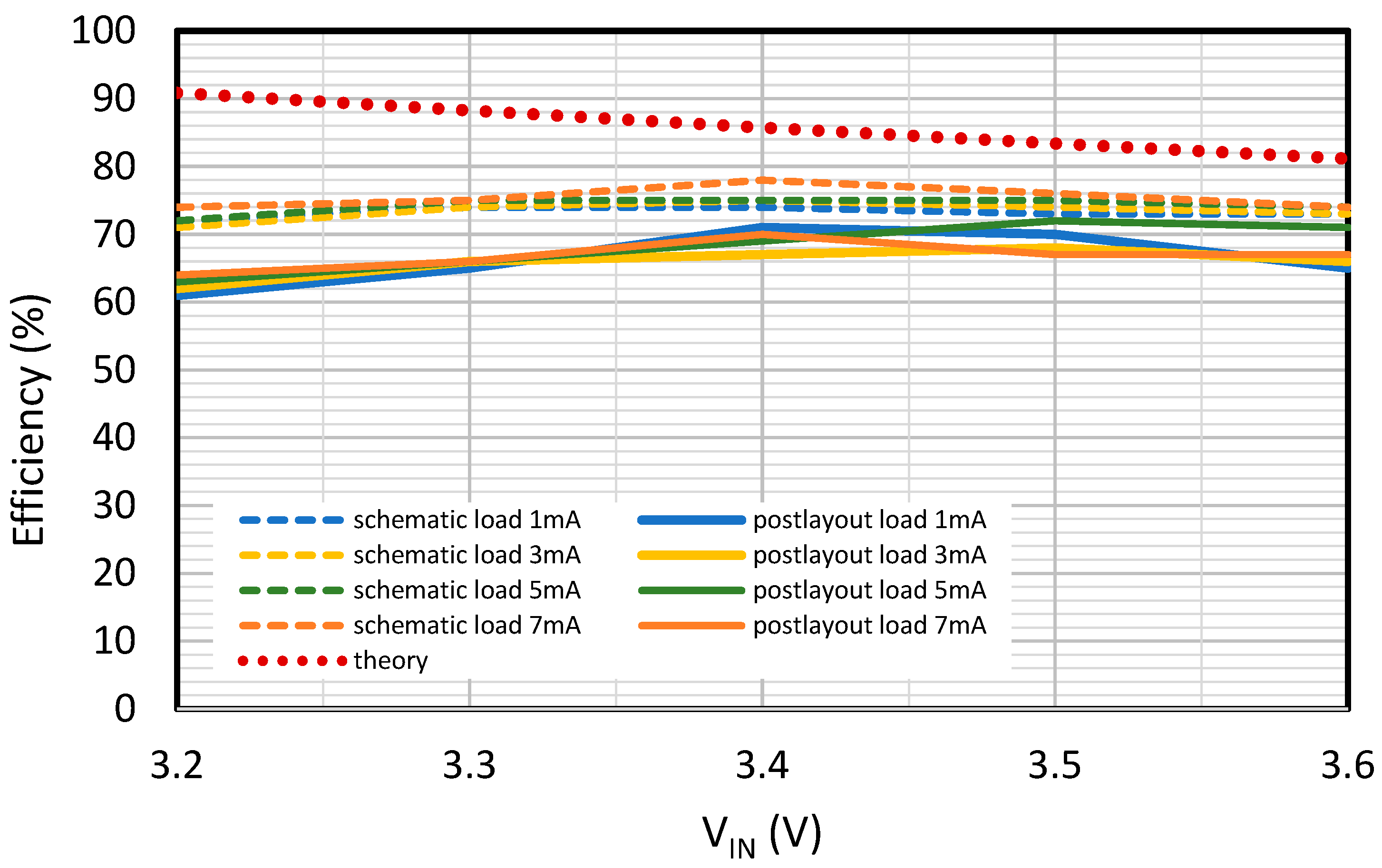
Figure 21.
Efficiency vs. input voltage for the buck mode (VOUT = 1.5 V).
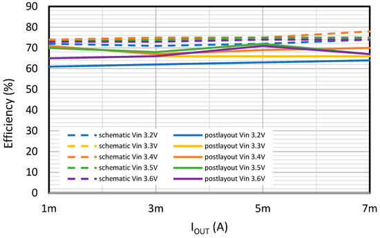
Figure 22.
Efficiency vs. load current for the buck mode (VOUT = 1.5 V).
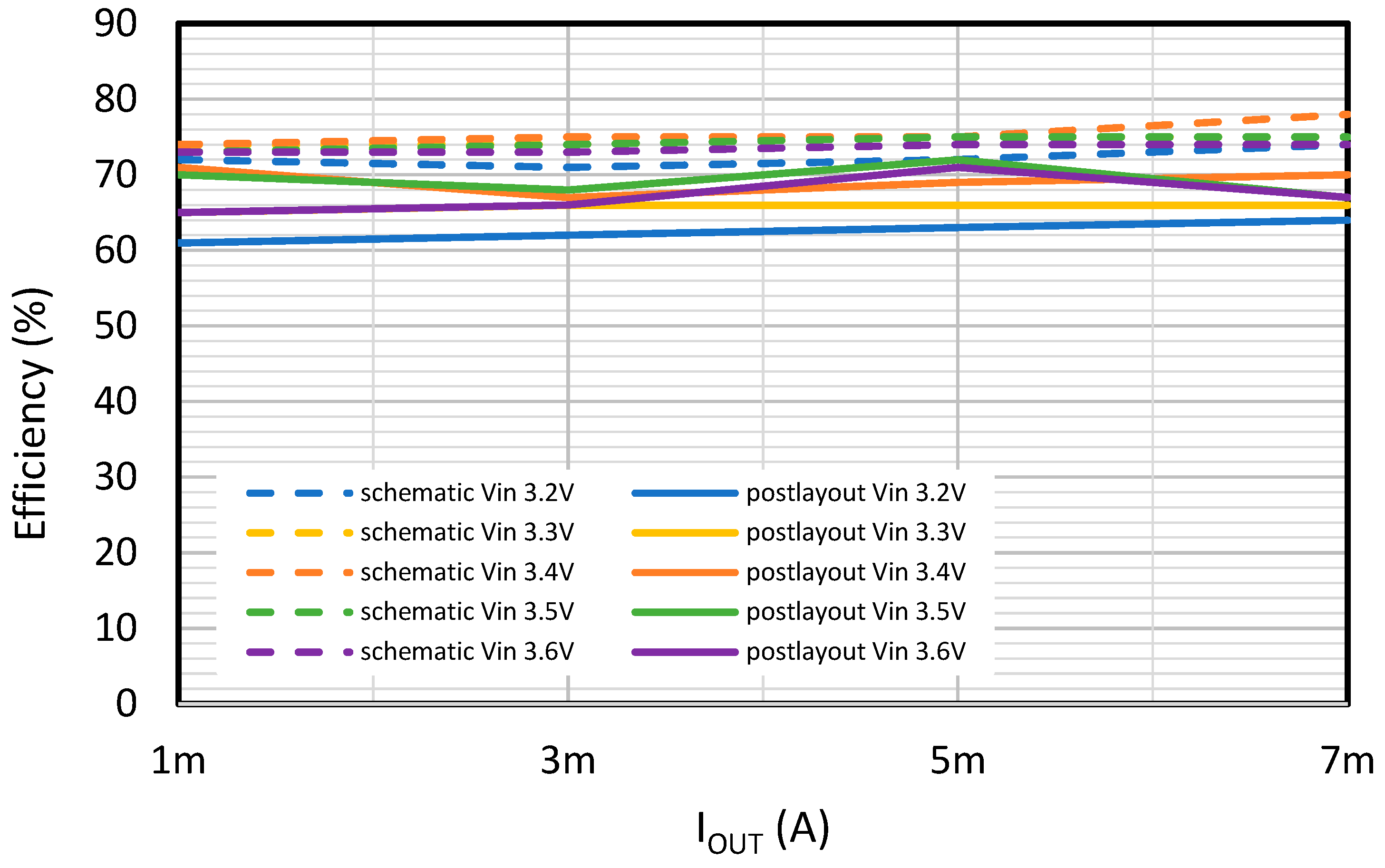
Figure 21 shows the efficiency levels of the CP in the buck mode over an input voltage range between 3.2 V and 3.6 V. For the buck mode, we can notice high simulation efficiency results and when the input voltage is 3.4 V, the CP succeeds at its optimum efficiency operating point. In Figure 22, the efficiency over different load currents is depicted. As can be observed, the schematic and postlayout measurements are quite similar and close to the theoretical expectations according to Equations (5) and (6). Based on Figure 20 and Figure 22, we can conclude that the efficiency levels are quite constant across different output load conditions for a specific input voltage.
4.3. Layout Considerations
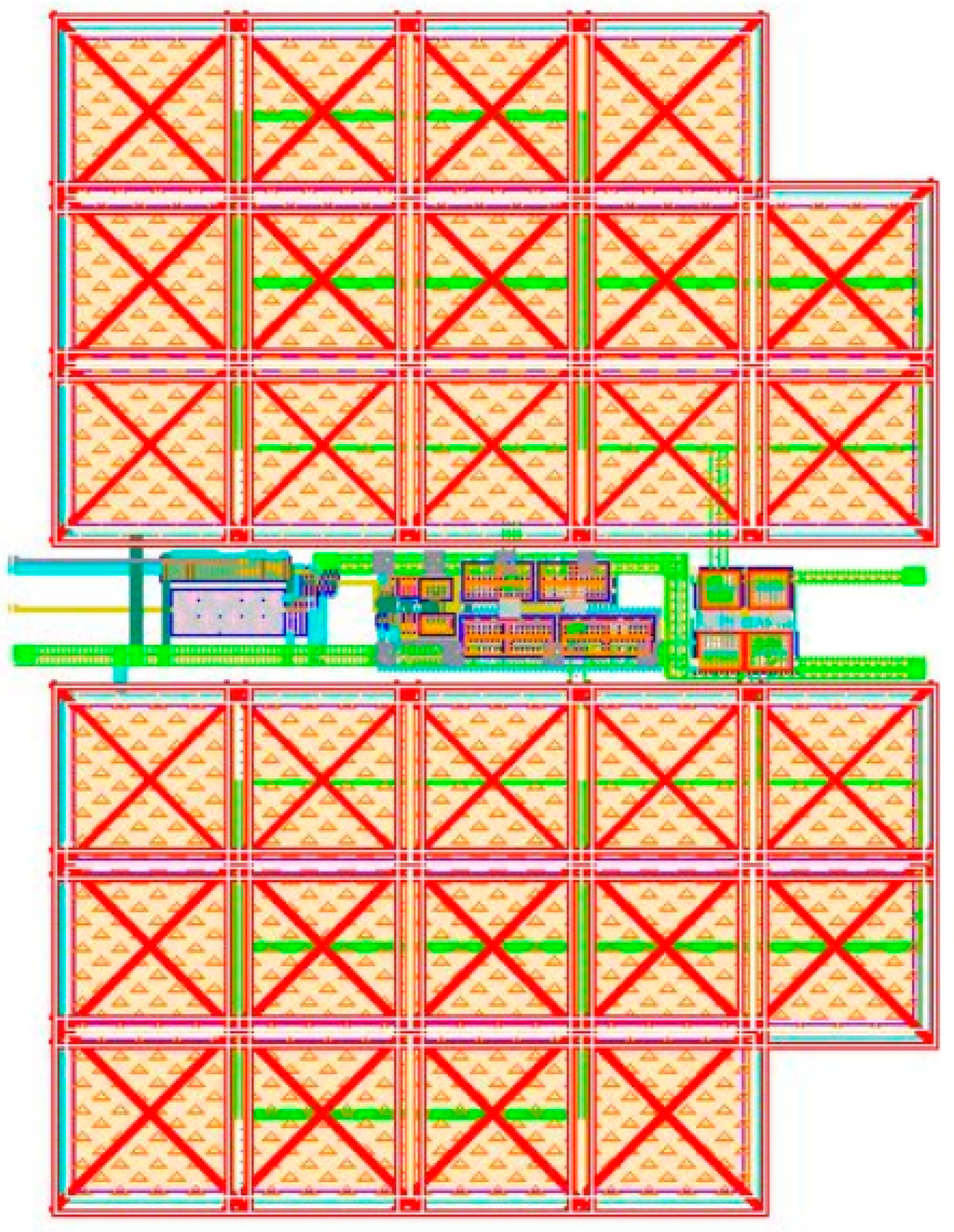
Finally, the layout of the proposed circuit is depicted in Figure 23. The proposed inductorless dual-mode buck-boost CP is fully integrated, occupies a small area on the die, and is easy to implement. For the design metal–insulator–metal (MIM), capacitors have been used because they introduce fewer parasitic capacitances and they do not affect the overall efficiency of the CP, in contrast to metal–oxide–metal (MOM) capacitors, for which simulations have shown that they affect the efficiency levels of the CP due to parasitic capacitances. Additionally, the flying capacitors need to be placed as close to the core of the CP and the outputs of the driver as possible and short traces for the interconnections must be used. Another critical factor that affects the efficiency and the conversion ratio of the design is the size of the devices that are used in the core of the CP and at the last stages of the driver that drives the flying capacitors and the core. They must be large enough to be able to drive the load at the output of the CP and at the same time, must preserve low enough consumption levels. Otherwise, the power efficiency of the system could be reduced considerably.

Figure 23.
Layout of the proposed buck-boost CP in TSMC 65 nm (769.4 μm × 551.2 μm).
4.4. Comparison with Other Topologies and Discussion
As was mentioned in Section 1, many CP topologies such as inductor-based and inductorless buck and/or boost can be found in the literature. Efficiency is one of the most critical parameters in CP design. In Table 1, our proposed work is compared to other realizations. In [3,4], the proposed architectures are inductor-based, so they use external inductors for the charge transferring and they implement both buck and boost modes. Most important is that they are for high-voltage applications, which do not suffer from mos threshold voltage and, therefore, they can provide high efficiency. In [14,15,16], switched-capacitor and fully integrated topologies are proposed, but only for step-up conversion. Finally, in [22], Kilani presents a switched-capacitor CP, fully integrated with high efficiency, for a wide input voltage range and specific output voltage levels. However, it is only a buck converter.

Table 1.
Efficiency comparison of our proposed buck-boost CP with other works from the literature.
It can be noticed from Table 1 that the inductor-based buck-boost topologies have higher efficiency levels than the inductorless CPs because they use external inductors. The required value of the inductors makes them unsuitable for integration and their external use makes the overall circuit bulky, which is an important disadvantage when the circuit must be compact.
On the other hand, there are many inductorless CPs, such as those in [14] or [22], which are fully integrated and present high efficiency results, but they implement only one of the two modes; they are only buck or boost. Our proposed switched-capacitor converter merges the two modes in one circuit with good efficiency results compared to the theoretical expectations. The benefits are design time reduction, area reduction, and design reuse.
5. Conclusions
A novel, high-efficiency, dual-mode buck-boost CP is presented in this paper. The proposed architecture is described in detail. First, we analyze the subcircuits that compose the converter and then we describe how the two modes are realized by only switching the external connections of the CP. For the boost mode, the input voltage varies from 1.2 V to 1.8 V and the output voltage is 1.8 V. For the buck mode, the corresponding input voltage range is from 3.2 V to 3.6 V and the output voltage is 1.5 V. The output voltage of both modes can be adjusted to another level with the aid of the comparator. Additionally, the operation and the simulated efficiency results are presented in this paper for each of the two modes over different input voltage levels and under different load conditions to verify the performance of the proposed architecture. The novelty of the presented CP is that one circuit uses the same blocks and, with a dual mode configuration, can merge two different modes, while at the same time being inductorless and keeping good efficiency that is close to the theoretical expectation. Only an interchange at the input–output connections is needed, thus minimizing the area the CP occupies on the die. The operation of the CP in each mode was verified using the Cadence Virtuoso tool. The dual-mode CP was designed in 65 nm CMOS technology. Overall, based on the simulation results and the small size area that the circuit occupies, we can conclude that it makes a good buck-boost DC-DC converter choice as it is an area-efficient circuit, is inductorless, has stable driving capability over a range of different load conditions, and has good efficiency levels at the same time.
Author Contributions
Conceptualization, E.K., G.S., S.V. and F.P.; methodology, E.K., G.S. and F.P.; software, E.K. and G.S.; validation, E.K., G.S. and F.P.; formal analysis, E.K. and G.S.; investigation, E.K., G.S. and F.P.; resources, E.K., G.S. and F.P.; data curation, E.K., G.S. and F.P.; writing—original draft preparation, G.S. and E.K.; writing—review and editing, E.K., G.S., F.P. and S.V.; visualization, G.S. and E.K.; supervision, G.S. and F.P.; project administration, G.S., E.K. and F.P. All authors have read and agreed to the published version of the manuscript.
Funding
This research received no external funding.
Institutional Review Board Statement
Not applicable.
Informed Consent Statement
Not applicable.
Data Availability Statement
All data are included within the manuscript.
Conflicts of Interest
The authors declare no conflict of interest.
References
- Ke-Horng, C. Energy-Harvesting Systems, in Power Management Techniques for Integrated Circuit Design; IEEE: Piscataway, NJ, USA, 2016; pp. 483–526. [Google Scholar] [CrossRef]
- Saharia, B. A comparative study on converter topologies for maximum power point tracking application in photovoltaic generation. J. Renew. Sustain. Energy 2014, 6, 053140. [Google Scholar] [CrossRef]
- Rodríguez-Lorente, A.; Barrado, A.; Calderón, C.; Fernández, C.; Lázaro, A. Non-inverting and Non-isolated Magnetically Coupled Buck-Boost Bidirectional DC–DC Converter. IEEE Trans. Power Electron. 2020, 35, 11942–11954. [Google Scholar] [CrossRef]
- Schaltz, E.; Rasmussen, P.O.; Khaligh, A. Non-inverting buck-boost converter for fuel cell applications. In Proceedings of the 2008 34th Annual Conference of IEEE Industrial Electronics, Orlando, FL, USA, 10–13 November 2008; pp. 855–860. [Google Scholar] [CrossRef]
- Abdel-Rahim, O.; Chub, A.; Blinov, A.; Vinnikov, D.; Peftitsis, D. An Efficient Non-Inverting Buck-Boost Converter with Improved Step Up/Down Ability. Energies 2022, 15, 4550. [Google Scholar] [CrossRef]
- Lai, C.-M.; Lin, W.-H.; Teh, J.; Mishima, T. An Interleaved Charge-Pump Bidirectional DC/DC Converter with Duty Limit Control Strategy. In Proceedings of the 4th International Conference on Electrical, Control and Instrumentation Engineering (ICECIE), Kuala Lumpur, Malaysia, 26 November 2022; pp. 1–5. [Google Scholar] [CrossRef]
- Andrade, P.; Alcaso, A.N.; Bento, F.; Marques Cardoso, A.J. Buck-Boost DC-DC Converters for Fuel Cell Applications in DC Microgrids—State-of-the-Art. Electronics 2022, 11, 3941. [Google Scholar] [CrossRef]
- Dickson, J.F. On-chip high-voltage generation in MNOS integrated circuits using an improved voltage multiplier technique. IEEE J. Solid-State Circuits 1976, 11, 374–378. [Google Scholar] [CrossRef]
- Wu, J.T.; Chang, K.L. MOS charge pumps for low-voltage operation. IEEE J. Solid-State Circuits 1998, 33, 592–597. [Google Scholar] [CrossRef]
- Shiau, M.S.; Hsieh, Z.H.; Hsieh, C.C.; Liu, H.Y.; Liu, D.G. A Novel Static CTS Charge Pump with Voltage Level Controller for DC-DC Converters. In Proceedings of the 2007 IEEE Conference on Electron Devices and Solid-State Circuits, Tainan, Taiwan, 20–22 December 2007; pp. 481–484. [Google Scholar] [CrossRef]
- D’Arrigo, S.D.; Imondi, G.; Santin, G.; Gill, M.; Cleavelin, R.; Spagliccia, S.; Tomassetti, E.; Lin, S.; Nguyen, A.; Shah, P.; et al. A 5 V-only 256 kbit CMOS flash EEPROM. In Proceedings of the IEEE International Solid-State Circuits Conference, 1989 ISSCC. Digest of Technical Papers, New York, NY, USA, 15–17 February 1989; pp. 132–133. [Google Scholar] [CrossRef]
- Turnquist, M.J.; de Streel, G.; Bol, D.; Hiienkari, M.; Koskinen, L. Effects of back-gate bias on switched-capacitor DC-DC converters in UTBB FD-SOI. In Proceedings of the 2014 SOI-3D-Subthreshold Microelectronics Technology Unified Conference (S3S), Millbrae, CA, USA, 6–9 October 2014; pp. 1–2. [Google Scholar] [CrossRef]
- Sawada, K.; Sugawara, Y.; Masui, S. An on-chip high-voltage generator circuit for EEPROMs with a power supply voltage below 2 V, Digest of Technical Papers. In Proceedings of the Symposium on VLSI Circuits, Kyoto, Japan, 8–10 June 1995; pp. 75–76. [Google Scholar] [CrossRef]
- Cheraghi Shirazi, N.; Jannesari, A.; Torkzadeh, P. Self-start-up fully integrated DC-DC step-up converter using body biasing technique for energy harvesting applications. AEU-Int. J. Electron. Commun. 2018, 95, 24–35. [Google Scholar] [CrossRef]
- Favrat, P.; Deval, P.; Declercq, M.J. A high-efficiency CMOS voltage doubler. IEEE J. Solid-State Circuits 1998, 33, 410–416. [Google Scholar] [CrossRef]
- Pelliconi, R.; Iezzi, D.; Baroni, A.; Pasotti, M.; Rolandi, P.L. Power efficient charge pump in deep submicron standard CMOS technology. In Proceedings of the 27th European Solid-State Circuits Conference, Villach, Austria, 18–20 September 2001; pp. 73–76. [Google Scholar]
- Keramida, E.; Souliotis, G.; Vlassis, S.; Plessas, F. Buck-Boost Charge Pump based DC-DC converter. In Proceedings of the 2022 Panhellenic Conference on Electronics & Telecommunications (PACET), Tripolis, Greece, 2–3 December 2022; pp. 1–5. [Google Scholar] [CrossRef]
- Ma, D.; Bondade, R. Fundamental Charge Pump Topologies and Design Principles. In Reconfigurable Switched-Capacitor Power Converters; Springer: New York, NY, USA, 2013. [Google Scholar] [CrossRef]
- Flores, Q.R.R.; Espinosa, F.V.G. Efficiency comparison of charge pump DC/DC configurations for energy harvesting. In Proceeding of the 2018 7th International Conference on Modern Circuits and Systems Technologies (MOCAST), Thessaloniki, Greece, 7–9 May 2018; pp. 1–4. [Google Scholar] [CrossRef]
- Tanzawa, T. Innovation of Switched-Capacitor Voltage Multiplier: Part 2: Fundamentals of the Charge Pump. IEEE Solid-State Circuits Mag. 2016, 8, 83–92. [Google Scholar] [CrossRef]
- Gunawardane, K.; Padmawansa, N.; Kularatna, N.; Subasinghage, K.; Lie, T.T. Current Context and Research Trends in Linear DC–DC Converters. Appl. Sci. 2022, 12, 4594. [Google Scholar] [CrossRef]
- Kilani, D.; Alhawari, M.; Mohammad, B.; Saleh, H.; Ismail, M. An Efficient Switched-Capacitor DC-DC Buck Converter for Self-Powered Wearable Electronics. IEEE Trans. Circuits Syst. I Regul. Pap. 2016, 63, 1557–1566. [Google Scholar] [CrossRef]
- Analog Devices. Available online: https://www.analog.com/media/en/training-seminars/design-handbooks/Practical-Design-Techniques-Power-Thermal/Section4.pdf (accessed on 20 February 2023).
- Palumbo, G.; Pappalardo, D. Charge Pump Circuits: An Overview on Design Strategies and Topologies. IEEE Circuits Syst. Mag. 2010, 10, 31–45. [Google Scholar] [CrossRef]
Disclaimer/Publisher’s Note: The statements, opinions and data contained in all publications are solely those of the individual author(s) and contributor(s) and not of MDPI and/or the editor(s). MDPI and/or the editor(s) disclaim responsibility for any injury to people or property resulting from any ideas, methods, instructions or products referred to in the content. |
© 2023 by the authors. Licensee MDPI, Basel, Switzerland. This article is an open access article distributed under the terms and conditions of the Creative Commons Attribution (CC BY) license (https://creativecommons.org/licenses/by/4.0/).


