
The Potential of SoC FPAAs for Emerging Ultra-Low-Power Machine Learning


Abstract
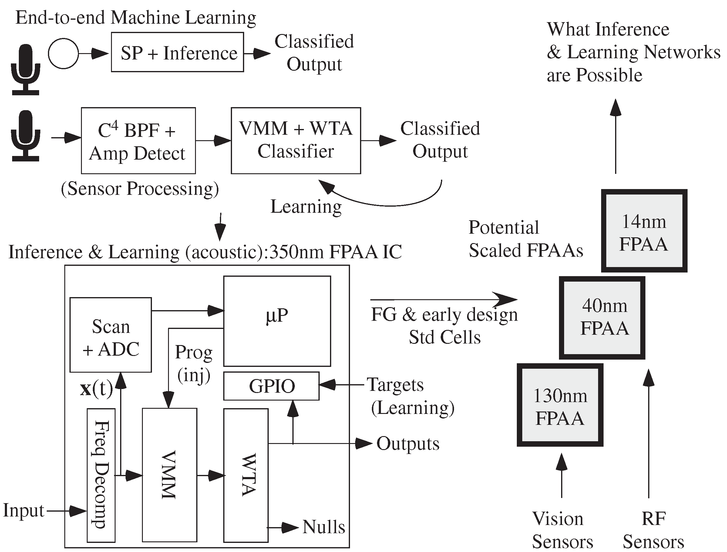
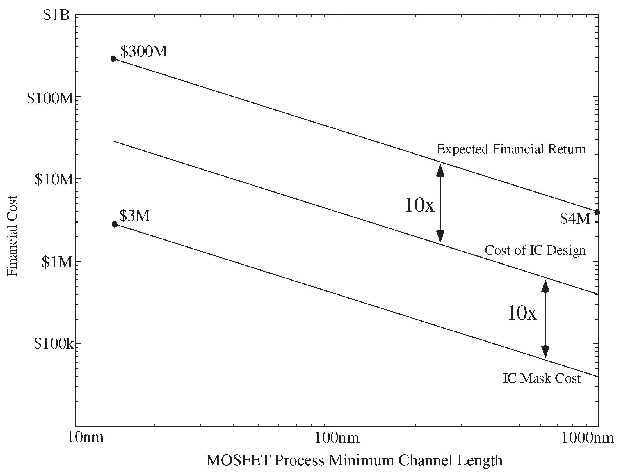
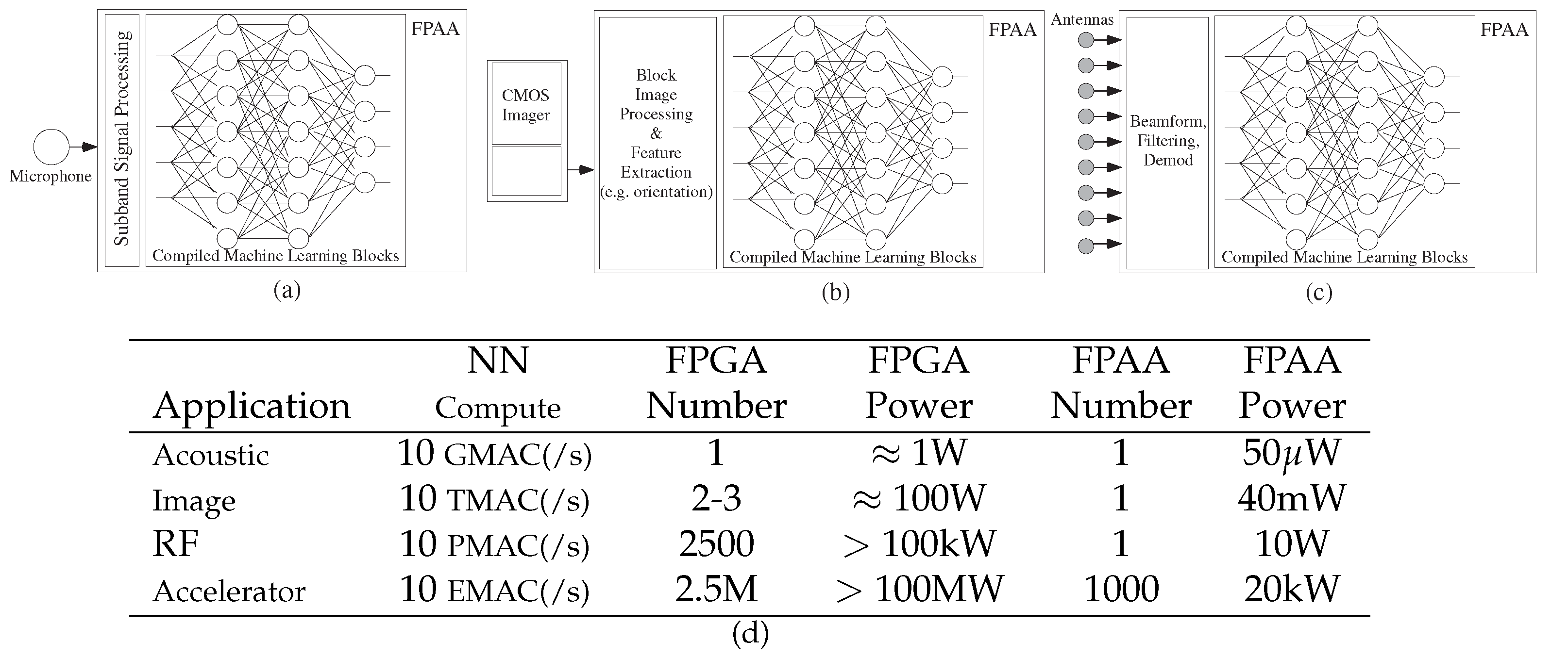
:1. Motivating Ultra-Low-Power Embedded Machine Learning
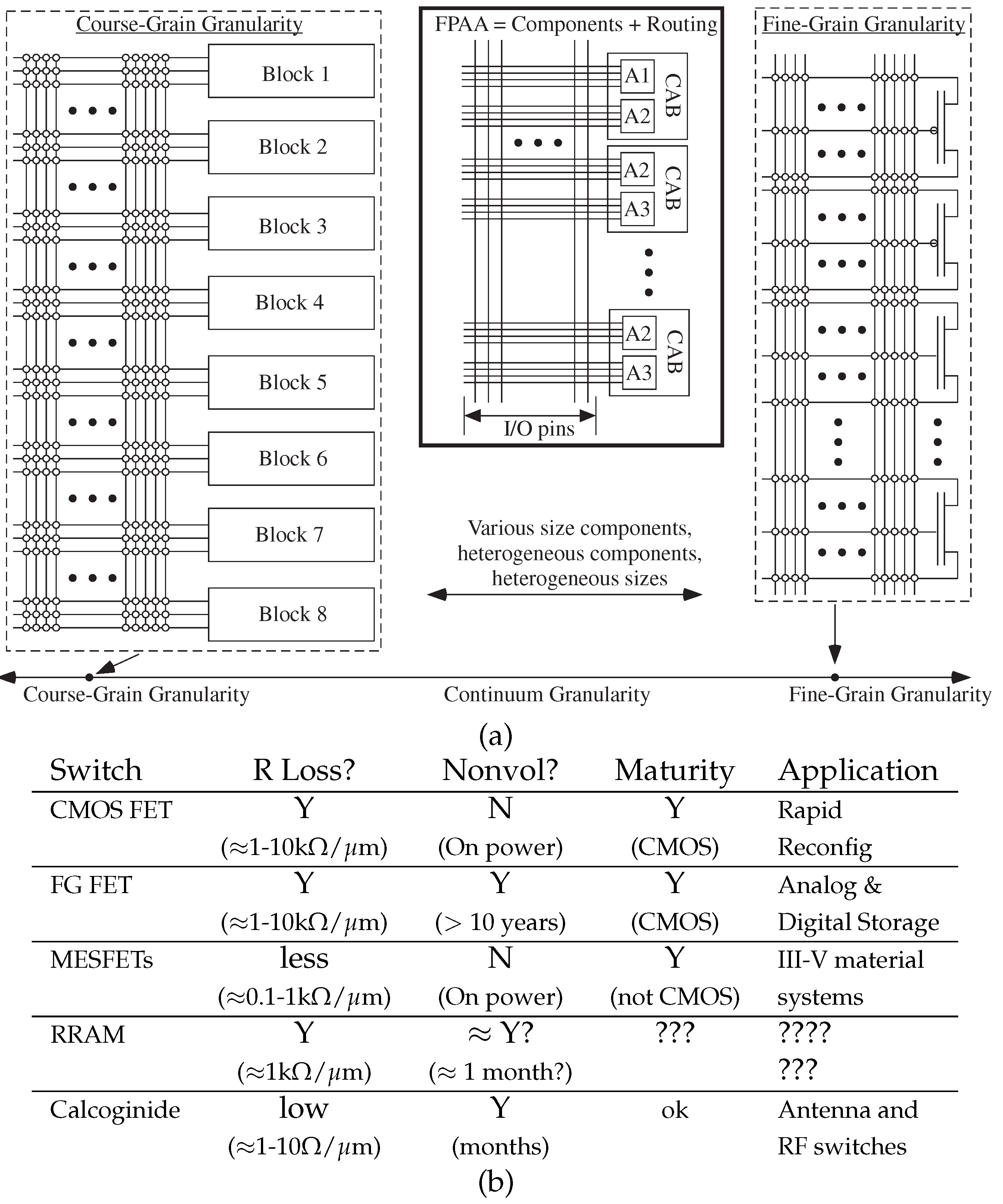
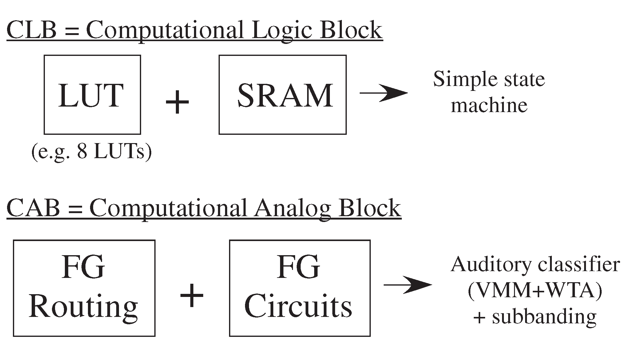
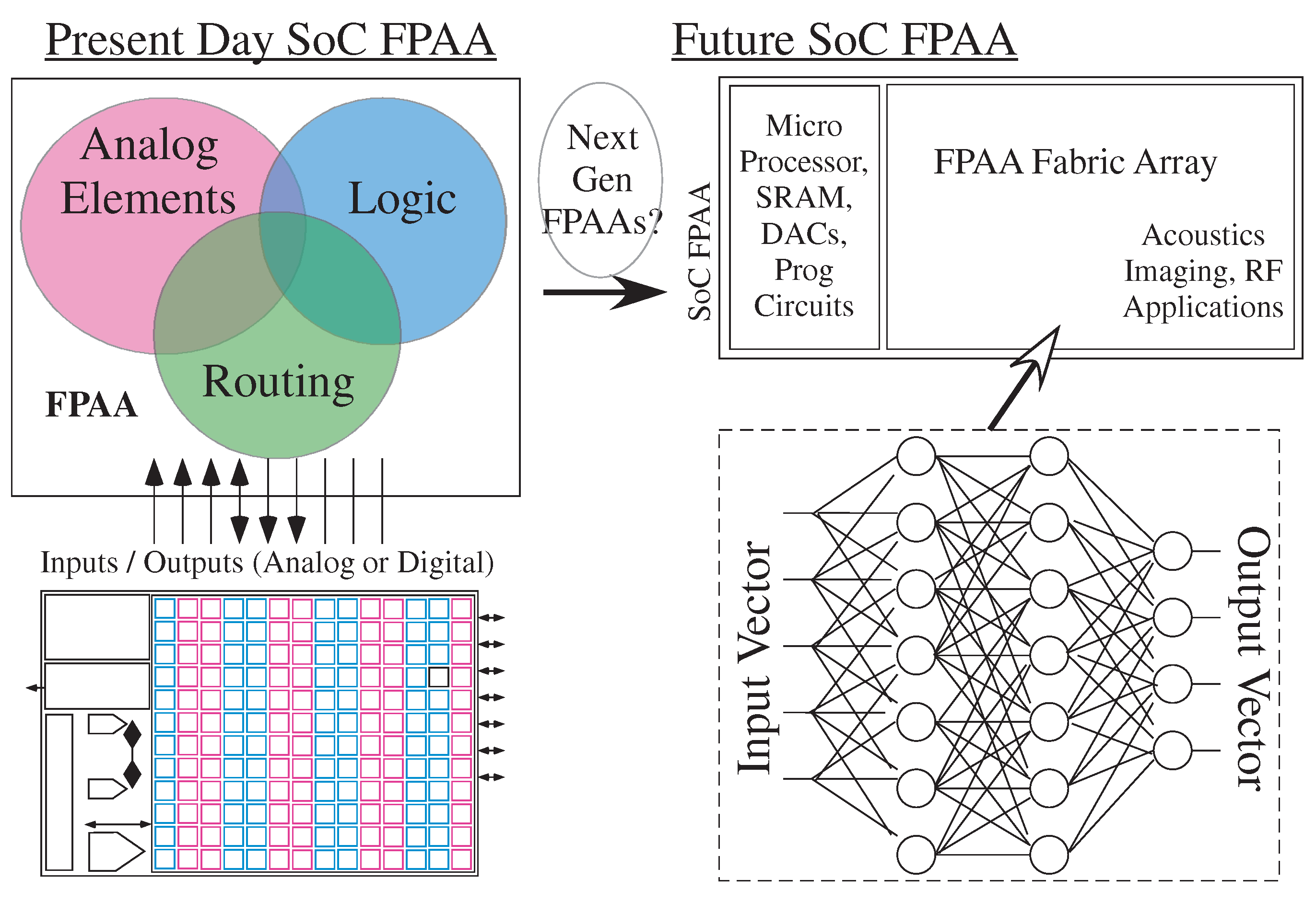
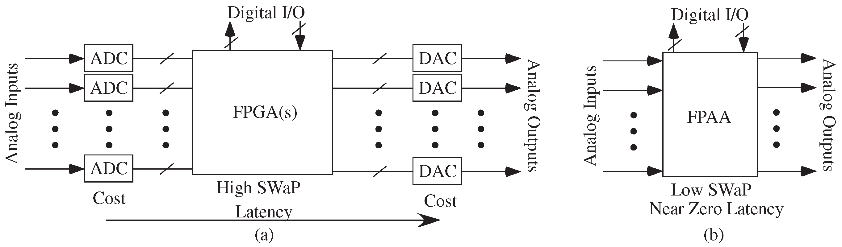
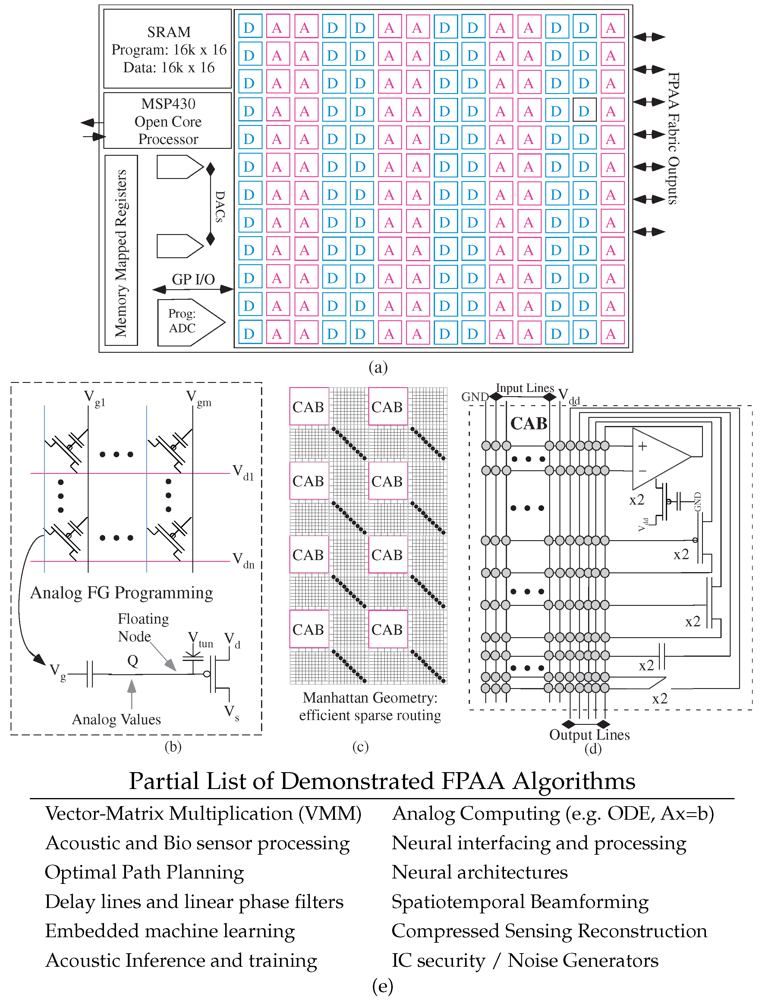
2. Configurable Technology, Architecture, and Capabilities
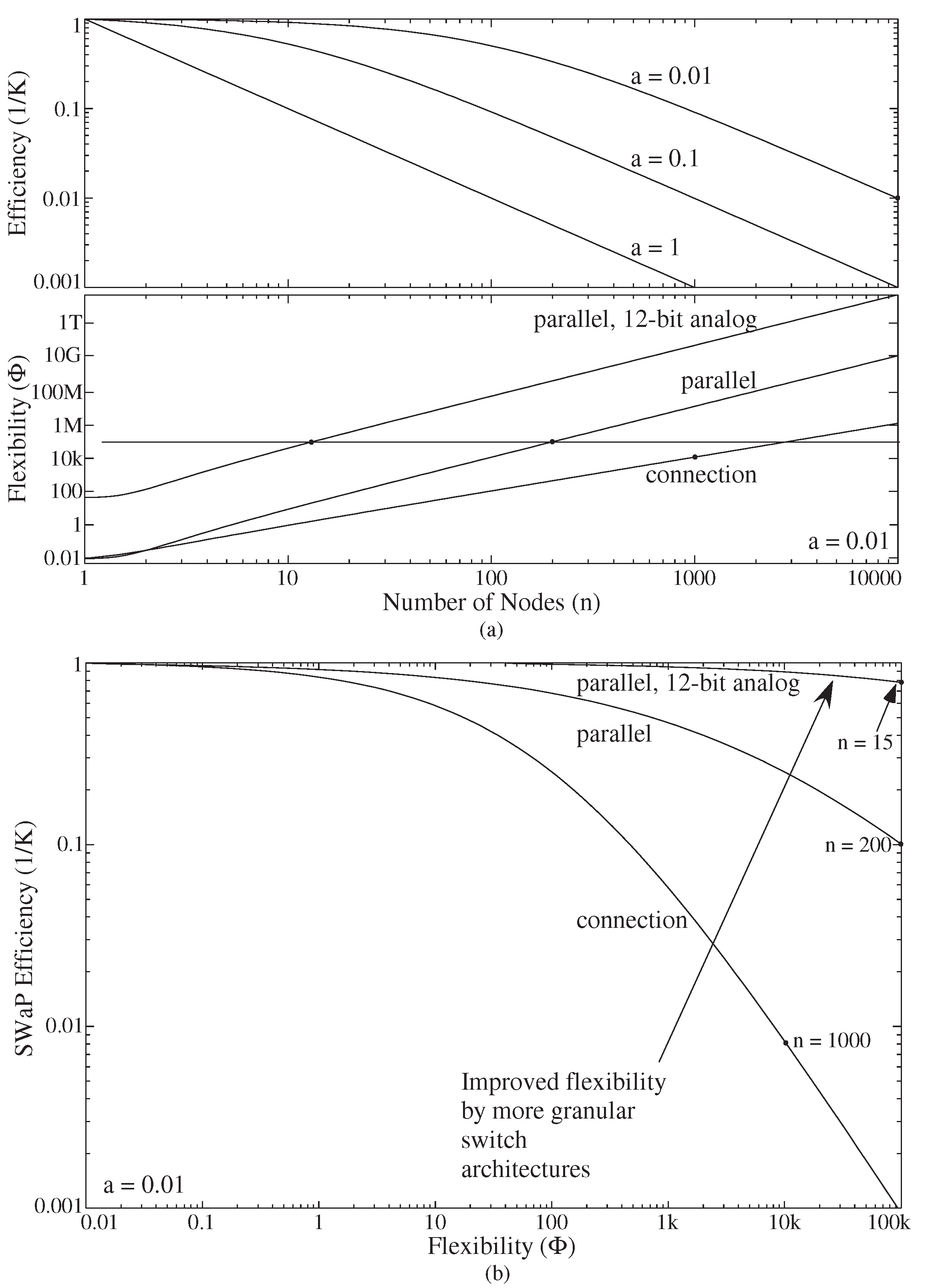
3. Granularity for End-To-End Machine Learning: Flexibility vs. Switch Cost
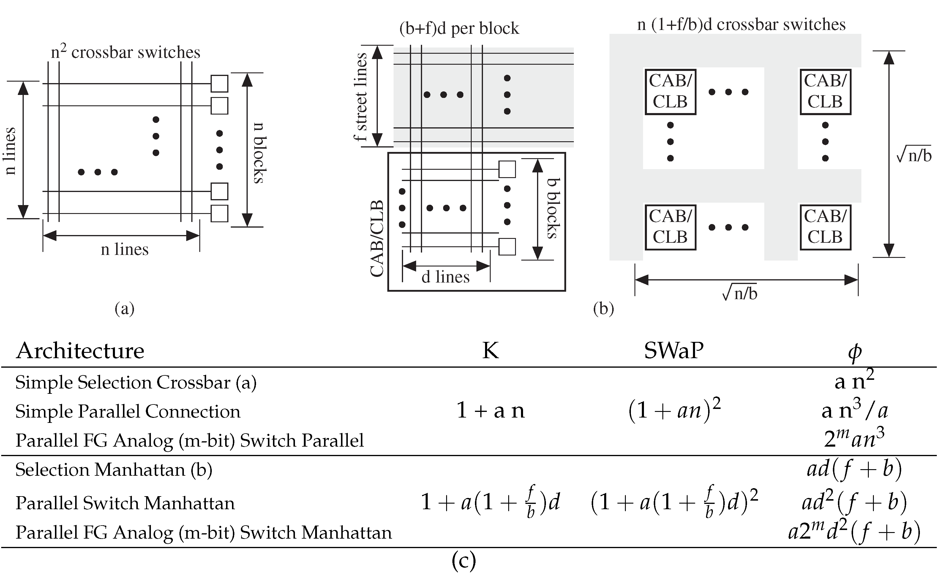
3.1. Course-Grain Architectures
3.2. Manhattan Architectures Improve Flexibility

3.3. Fine-Grain Architectures
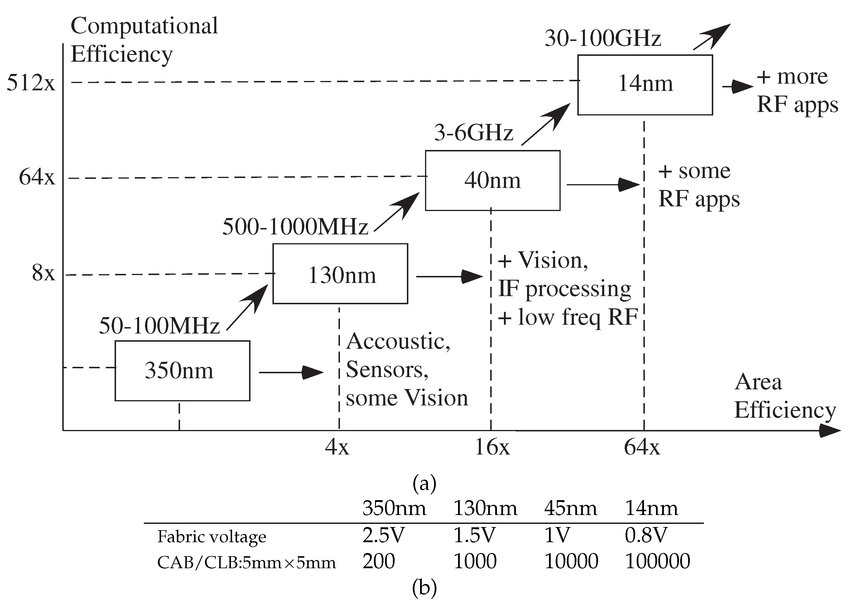
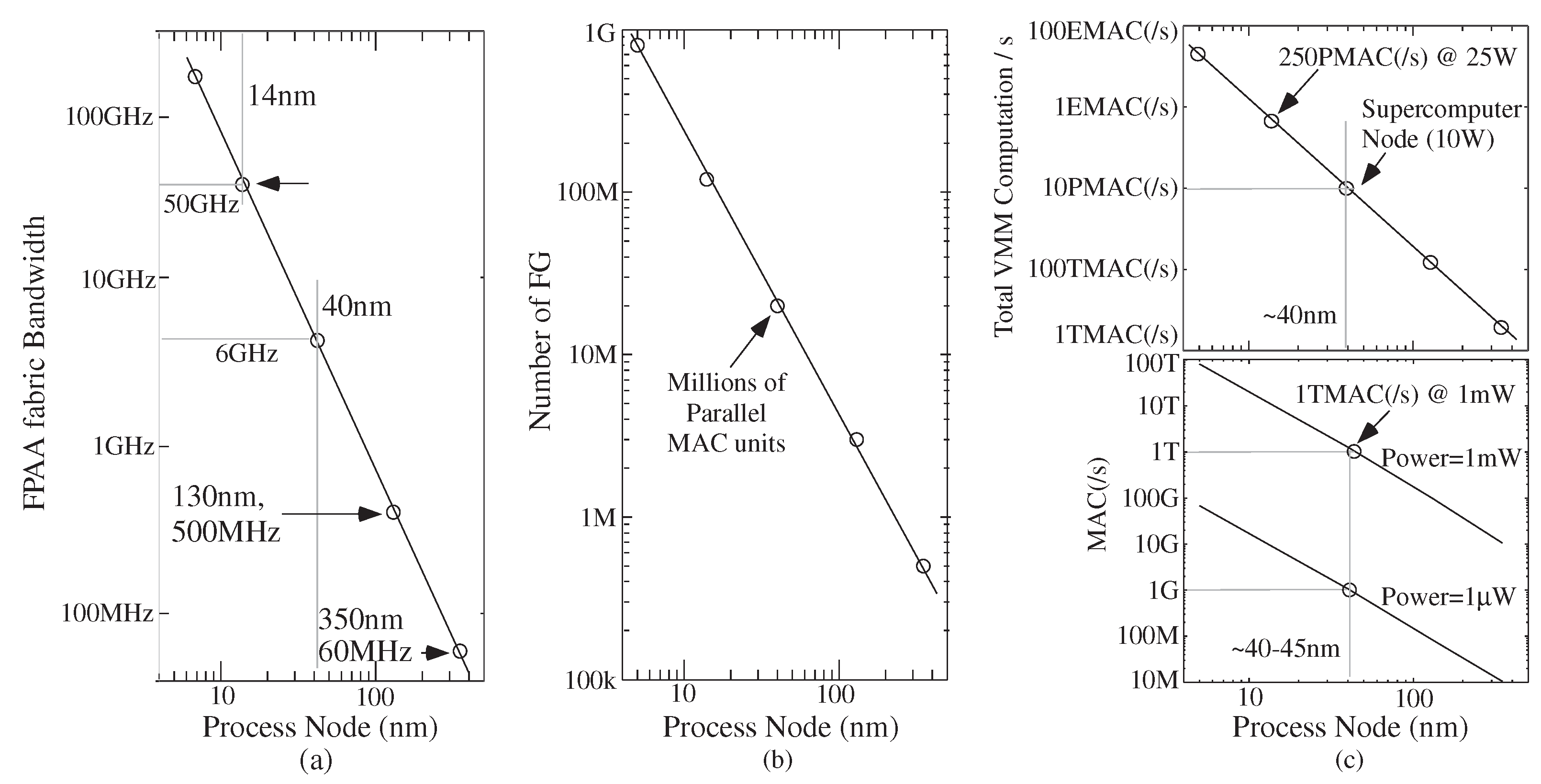
4. Scaled FPAA Devices Opportunities towards Low-Energy Machine Learning
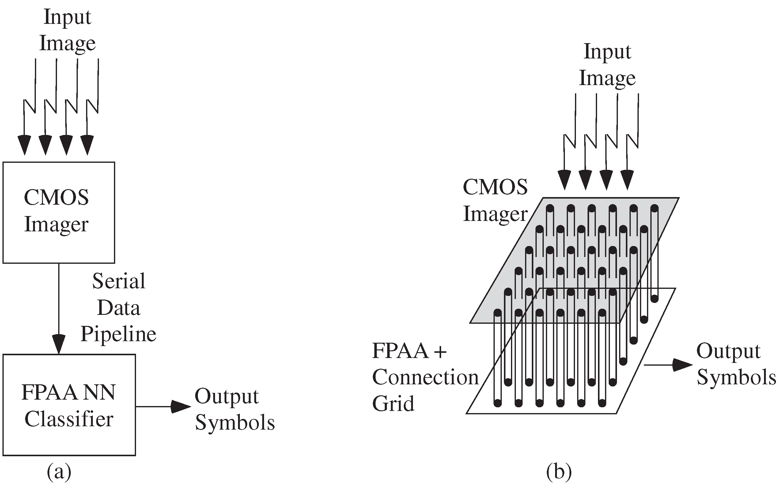
4.1. Machine Learning Computation Opportunities from Scaled CMOS FPAAs
4.2. Algorithm Opportunities from Scaled CMOS FPAAs
5. Summary and Further Directions
Funding
Data Availability Statement
Conflicts of Interest
References
- Hasler, J. Large-Scale Field Programmable Analog Arrays. Proc. IEEE 2020, 108, 1283–1302. [Google Scholar] [CrossRef]
- Hasler, J.; Shah, S. Learning for VMM + WTA Embedded Classifiers. In Proceedings of the GOMAC, Orlando, FL, USA, 14–17 March 2016. [Google Scholar]
- Hasler, J.; Shah, S. SoC FPAA Hardware Implementation of a VMM+WTA Embedded Learning Classifier. IEEE J. Emerg. Sel. Top. Circuits Syst. 2018, 8, 28–37. [Google Scholar]
- Hasler, J.; Shah, S. VMM + WTA Embedded Classifiers Learning Algorithm implementable on SoC FPAA devices. IEEE J. Emerg. Sel. Top. Circuits Syst. 2018, 8, 65–76. [Google Scholar] [CrossRef]
- Thompson, N.C.; Greenewald, K.; Lee, K.; Manso, G.F. Deep Learning’s Diminishing Returns: The Cost of Improvement is Becoming Unsustainable. IEEE Spectr. 2021, 58, 50–55. [Google Scholar] [CrossRef]
- Mead, C. Neuromorphic electronic systems. Proc. IEEE 1990, 78, 1629–1636. [Google Scholar] [CrossRef] [Green Version]
- Chawla, R.; Bandyopadhyay, A.; Srinivasan, V.; Hasler, A. 531 nW/MHz, 128 × 32 current-mode programmable analog vector-matrix multiplier with over two decades of linearity. In Proceedings of the IEEE Custom Integrated Circuits Conference, Orlando, FL, USA, 6 October 2004; pp. 651–654. [Google Scholar]
- Schlottmann, C.; Hasler, P. A highly dense, low power, programmable analog vector-matrix multiplier: The FPAA implementation. IEEE J. Emerg. Sel. Top. Circuits Syst. 2011, 1, 403–411. [Google Scholar] [CrossRef]
- Hasler, J.; Marr, H.B. Finding a Roadmap to achieve Large Neuromorphic Hardware Systems. Front. Neuromorphic Eng. 2013, 7, 1–29. [Google Scholar] [CrossRef] [Green Version]
- Rosenblatt, F. The perceptron: A probabilistic model for information storage and organization in the brain. Psychol. Rev. 1958, 65, 386–408. [Google Scholar] [CrossRef] [Green Version]
- Widrow, B.; Hoff, M.E. Adaptive switching circuits. IRE WESCON Conv. 1960, 4, 96–140. [Google Scholar]
- Hasler, J.; Black, E. Physical Computing: Unifying Real Number Computation. J. Low Power Electron. Appl. 2021, 11, 14. [Google Scholar] [CrossRef]
- Hall, T.; Twigg, C.; Gray, J.; Hasler, P.; Anderson, D. Large-scale field-programmable analog arrays for analog signal processing. IEEE Trans. Circuits Syst. I 2005, 52, 2298–2307. [Google Scholar] [CrossRef]
- EE Times. Specifically Generic Analog Functions for FPAAs Anadigm Says. Available online: https://www.eetimes.com/specifically-generic-analog-functions-for-fpaas/ (accessed on 15 February 2022).
- Kuon, I.; Tessier, R.; Rose, J. FPGA Architecture: Survey and Challenges. Found. Trends Electron. Des. Autom. 2007, 2, 135–253. [Google Scholar] [CrossRef]
- Nguyen, M.; Serafin, N.; Hoe, J.C. Partial Reconfiguration for Design Optimization. In Proceedings of the IEEE International Conference on Field-programmable Logic and Applications (FPL), Gothenburg, Sweden, 31 August–4 September 2020. [Google Scholar]
- Chung, E.S.; Milder, P.A.; Hoe, J.C.; Mai, K. Single-chip Heterogeneous Computing: Does the future include Custom Logic, FPGAs, and GPUs? In Proceedings of the 2010 43rd Annual IEEE/ACM International Symposium on Microarchitecture, Atlanta, GA, USA, 4–8 December 2010; pp. 53–64. [Google Scholar]
- Chung, E.S.; Hoe, J.C.; Mai, K. CoRAM: An In-Fabric Memory Architecture for FPGA-based Computing. In Proceedings of the ACM Field-Programmable Gate Arrays (FPGA), Monterey, CA, USA, 27 February–1 March 2011; pp. 97–106. [Google Scholar]
- Farooq, U.; Marrakchi, Z.; Mehrez, H. FPGA Architectures: An Overview. In Tree-Based Heterogeneous FPGA Architectures; Springer: New York, NY, USA, 2012; pp. 7–48. [Google Scholar]
- Nguyen, M.; Tamburo, R.; Narasimhan, S.; Hoe, J.C. Quantifying the Benefits of Dynamic Partial Reconfiguration for Embedded Vision Applications. In Proceedings of the Field-Programmable Logic and Applications (FPL), Barcelona, Spain, 8–12 September 2019. [Google Scholar]
- Boutros, A.; Nurvitadhi, E.; Ma, R.; Gribok, S.; Zhao, Z.; Hoe, J.C.; Betz, V.; Langhammer, M. Beyond Peak Performance: Comparing the Real Performance of AI-Optimized FPGAs and GPUs. In Proceedings of the Field-Programmable Technology (FPT), Maui, HI, USA, 9–11 December 2020. [Google Scholar]
- Boutros, A.; Betz, V. FPGA Architecture: Principles and Progression. IEEE Circuits Syst. Mag. 2021, 21, 4–29. [Google Scholar] [CrossRef]
- Nikoli, S.; Tkei, Z.; Lenne, P.; Catthoor, F. Global Is the New Local: FPGA Architecture at 5 nm and Beyond. In Proceedings of the 2021 ACM/SIGDA International Symposium on Field-Programmable Gate Arrays, Virtual, 28 February–2 March 2021. [Google Scholar]
- Zynq UltraScale + RFSoC Data Sheet. Xlinix. DS889 v. 1.13. 7 January 2022. Available online: https://www.xilinx.com/support/documentation/data_sheets/ds889-zynq-usp-rfsoc-overview.pdf (accessed on 20 January 2022).
- Marr, B.; Degnan, B.; Hasler, P.; Anderson, D. Scaling energy per operation via an asynchronous pipeline. IEEE Trans. Very Large Scale Integr. (VLSI) Syst. 2013, 21, 147–151. [Google Scholar] [CrossRef]
- IGLOO2 FPGA, Microsemi. Available online: https://www.microsemi.com/product-directory/fpgas/1688-igloo2 (accessed on 8 May 2021).
- Available online: https://www.microsemi.com/product-directory/antifuse-fpgas/1700-axcelerator (accessed on 8 May 2021).
- George, S.; Kim, S.; Shah, S.; Hasler, J.; Collins, M.; Adil, F.; Wunderlich, R.; Nease, S.; Ramakrishnan, S. A Programmable and Configurable Mixed-Mode FPAA SoC. IEEE Trans. Very Large Scale Integr. (VLSI) Syst. 2016, 24, 2253–2261. [Google Scholar] [CrossRef]
- Kim, S.; Hasler, J.; George, S. Integrated Floating-Gate Programming Environment for System-Level Ics. IEEE Trans. Very Large Scale Integr. (VLSI) Syst. 2016, 24, 2244–2252. [Google Scholar] [CrossRef]
- Srinivasan, V.; Serrano, G.; Twigg, C.; Hasler, P. A Floating-Gate-Based Programmable CMOS Reference. IEEE Trans. Circuits Syst. I 2008, 55, 3448–3456. [Google Scholar] [CrossRef]
- Collins, M.; Hasler, J.; George, S. An Open-Source Toolset Enabling Analog–Digital–Software Codesign. invited paper. J. Low Power Electron. Appl. 2016, 6, 3. [Google Scholar] [CrossRef]
- Kim, S.; Shah, S.; Wunderlich, R.; Hasler, J. CAD Synthesis Tools for Large-Scale Floating-Gate FPAA System. J. Des. Autom. Embed. Syst. 2021, 25, 1–16. [Google Scholar]
- Hasler, J. A CMOS Programmable Analog Standard Cell Library in Skywater 130 nm Open-Source Process. In Proceedings of the Workshop on Open-Source EDA Technology, WOSET, Virtual, 4 November 2021. [Google Scholar]
- Hasler, J.; Shah, S. Security Implications for Ultra-Low Power Configurable Analog and Mixed Mode SoC Systems. J. Low Power Electron. Appl. 2018, 8, 17. [Google Scholar] [CrossRef] [Green Version]
- Nease, S.; Lanterman, A.; Hasler, J. A Transistor Ladder Voltage-Controlled Filter Implemented on a Field Programmable Analog Array. J. Audio Eng. Soc. 2014, 62, 611–618. [Google Scholar] [CrossRef]
- Keymeulen, D.; Zebulum, R.S.; Jin, Y.; Stoica, A. Fault-tolerant evolvable hardware using field-programmable transistor arrays. IEEE Trans. Reliab. 2000, 49, 305–316. [Google Scholar] [CrossRef] [Green Version]
- Stoica, A.; Zebulum, R.; Keymeulen, D.; Tawel, R.; Daud, T.; Thakoor, A. Reconfigurable VLSI architectures for evolvable hardware: From experimental field programmable transistor arrays to evolution-oriented chips. IEEE Trans. Very Large Scale Integr. (VLSI) Syst. 2001, 9, 227–232. [Google Scholar] [CrossRef]
- Gaudet, V.; Gulak, G. 10 MHz field programmable analog array prototype based on CMOS current conveyors. Proceedings of 1999 Micronet Annual Workshop, Ottawa, ON, Canada, 26–17 April 1999. [Google Scholar]
- Lee, E.K.F.; Gulak, P.G. Field programmable analogue array based on MOSFET transconductors. Electron. Lett. 1992, 28, 28–29. [Google Scholar] [CrossRef]
- Klein, H.W. The EPAC architecture: An expert cell approach to field programmable analog circuits. In Proceedings of the 39th Midwest Symposium on Circuits and Systems, Ames, IA, USA, 21 August 1996; Volume 1, pp. 169–172. [Google Scholar]
- Becker, J.; Manoli, Y. A continuous-time field programmable analog array (FPAA) consisting of digitally reconfigurable GM-cells. In Proceedings of the 2004 IEEE International Symposium on Circuits and Systems (IEEE Cat. No. 04CH37512), Vancouver, BC, Canada, 23–26 May 2004; pp. I.1092–I.1095. [Google Scholar]
- Cowan, G.E.R.; Melville, R.C.; Tsividis, Y.P. A VLSI analog computer/digital computer accelerator. IEEE J. Solid-State Circuits 2006, 41, 42–53. [Google Scholar] [CrossRef]
- Guo, N.; Huang, Y.; Mai, T.; Patil, S.; Cao, C.; Seok, M.; Sethumadhavan, S.; Tsividis, Y. Energy-efficient hybrid analog/digital approximate computation in continuous time. IEEE J. Solid-State Circuits 2016, 51, 1514–1524. [Google Scholar] [CrossRef]
- Huang, Y.; Guo, N.; Seok, M.; Tsividis, Y.; Mandli, K.; Sethumadhavan, S. Hybrid analog-digital solution of nonlinear partial differential equations. In Proceedings of the 2017 50th Annual IEEE/ACM International Symposium on Microarchitecture (MICRO), Boston, MA, USA, 14–17 October 2017; pp. 665–678. [Google Scholar]
- Kelly, B.M.; Rumberg, B.; Graham, D.W.; Kulathumani, V. Reconfigurable analog signal processing for wireless sensor networks. In Proceedings of the 2013 IEEE 56th International Midwest Symposium on Circuits and Systems (MWSCAS), Columbus, OH, USA, 4–7 August 2013; pp. 221–224. [Google Scholar]
- Rumberg, B.; Graham, D.W.; Clites, S.; Kelly, B.M.; Navidi, M.M.; Dilello, A.; Kulathumani, V. RAMP: Accelerating wireless sensor hardware design with a reconfigurable analog/mixed-signal platform. In Proceedings of the 14th International Conference on Information Processing in Sensor Networks, Seattle, WA, USA, 13–16 April 2015; pp. 47–58. [Google Scholar]
- Rumberg, B.; Graham, D.W. A low-power field-programmable analog array for wireless sensing. In Proceedings of the Sixteenth International Symposium on Quality Electronic Design, Santa Clara, CA, USA, 2–4 March 2015; pp. 542–546. [Google Scholar]
- Kim, K.H.; Gaba, S.; Wheeler, D.; Cruz-Albrecht, J.M.; Hussain, T.; Srinivasa, N.; Lu, W. A functional hybrid memristor crossbar-array/CMOS system for data storage and neuromorphic applications. Nano Lett. 2012, 12, 389–395. [Google Scholar] [CrossRef]
- Jo, S.H.; Kim, K.H.; Lu, W. Short-term memory to long-term memory transition in a nanoscale memristor. ACS Nano 2011, 9, 7669–7676. [Google Scholar]
- Jo, S.H.; Lu, W. Programmable resistance switching in nanoscale two-terminal devices. Nano Lett. 2009, 9, 496–500. [Google Scholar] [CrossRef]
- Snider, G.; Amerson, R.; Carter, D.; Abdalla, H.; Qureshi, M.S.; Leveille, J.; Versace, M.; Ames, H.; Patrick, S.; Chandler, B.; et al. From synapses to circuitry: Using memristive memory to explore the electronic brain. IEEE Comput. 2011, 44, 21–28. [Google Scholar] [CrossRef]
- Pohm, A.; Sie, C.; Uttecht, R.; Kao, V.; Agrawal, O. Chalcogenide glass bistable resistivity (Ovonic) memories. IEEE Trans. Magn. 1970, 6, 592. [Google Scholar] [CrossRef]
- Lee, B.C.; Ipek, E.; Mutlu, O.; Burger, D. Architecting phase change memory as a scalable dram alternative. In Proceedings of the 36th Annual International Symposium on Computer Architecture, Austin, TX, USA, 15 June 2009. [Google Scholar]
- Karpov, I.V.; Kencke, D.; Kau, D.; Tang, S.; Spadini, G. Phase Change Memory with Chalcogenide Selector (PCMS): Characteristic Behaviors, Physical Models and Key Material Properties. MRS Online Proc. Libr. 2010, 1250, 701. [Google Scholar]
- Burr, G.W.; Breitwisch, M.J.; Franceschini, M.; Garetto, D.; Gopalakrishnan, K.; Jackson, B.; Kurdi, B.; Lam, C.; Lastras, L.A.; Padilla, A.; et al. Phase change memory technology. J. Vac. Sci. Technol. B 2010, 28, 223–262. [Google Scholar] [CrossRef] [Green Version]
- Chung, H.; Jeong, B.H.; Min, B.J.; Choi, Y.; Cho, B.H.; Shin, J.; Kim, J.; Sunwoo, J.; Park, J.; Wang, Q.; et al. A 58 nm 1.8V 1Gb PRAM with 6.4MB/s program BW. In Proceedings of the 2011 IEEE International Solid-State Circuits Conference, San Francisco, CA, USA, 20–24 February 2011; pp. 500–502. [Google Scholar]
- Xu, Z.; Sutaria, K.B.; Yang, C.; Chakrabarti, C.; Cao, Y. Hierarchical modeling of Phase Change memory for reliable design. In Proceedings of the 2012 IEEE 30th International Conference on Computer Design (ICCD), Montreal, QC, Canada, 30 September–3 October 2012; pp. 115–120. [Google Scholar]
- Choi, Y.; Song, I.; Chung, M.H.P.H.; Chang, S.; Cho, B.; Kim, J.; Oh, Y.; Kwon, D.; Sunwoo, J.; Shin, J.; et al. A 20 nm 1.8V 8Gb PRAM with 40 MB/s program bandwidth. In Proceedings of the 2012 IEEE International Solid-State Circuits Conference. San Francisco, CA, USA, 19–23 February 2012. [Google Scholar]
- di Ventra, M.; Pershin, Y.V. On the physical properties of memristive, memcapacitive and meminductive systems. Nanotechnology 2013, 24, 25. [Google Scholar] [CrossRef] [Green Version]
- Raoux, S.; Xiong, F.; Wuttig, M.; Pop, E. Phase change materials and phase change memory. MRS Bull. Mater. Res. Soc. 2014, 39, 703–710. [Google Scholar] [CrossRef] [Green Version]
- Le Gallo, M.; Sebastian, A. An overview of phase-change memory device physics. J. Phys. D Appl. Phys. 2020, 53, 1–27. [Google Scholar] [CrossRef]
- Song, S.; Mutlu, O.; Das, A.; Kandasamy, N. Improving Phase Change Memory Performance with Data Content Aware Access. In Proceedings of the 2020 ACM SIGPLAN International Symposium on Memory Management, London, UK, 16 June 2020. [Google Scholar]
- Kushner, L.J.; Sliech, K.W.; Flewelling, G.M.; Cali, J.D.; Grens, C.M.; Turner, S.E.; Jansen, D.S.; Wood, J.L.; Madison, G.M. The MATRICs RF-FPGA in 180 nm SiGe-on-SOI BiCMOS. In Proceedings of the IEEE RFIC Symposium, Phoenix, AZ, USA, 17–19 May 2015; pp. 283–286. [Google Scholar]
- Trimberger, S. Three ages of FPGAs: A retrospective on the first thirty years of FPGA technology. Proc. IEEE 2015, 103, 3. [Google Scholar] [CrossRef]
- Twigg, C.; Gray, J.D.; Hasler, P. Programmable floating gate FPAA switches are not dead weight. In Proceedings of the IEEE International Symposium on Circuits and Systems, New Orleans, LA, USA, 27–30 May 2007; pp. 169–172. [Google Scholar]
- Kucic, M.; Hasler, P.; Dugger, J.; Anderson, D. Programmable and adaptive analog filters using arrays of floating-gate circuits. In Proceedings of the 2001 Conference on Advanced Research in VLSI. ARVLSI 2001, Salt Lake City, UT, USA, 14–16 March 2001; pp. 148–162. [Google Scholar]
- Hasler, J.; Kim, S.; Adil, F. Scaling Floating-Gate Devices Predicting Behavior for Programmable and Configurable Circuits and Systems. J. Low Power Electron. Appl. 2016, 6, 13. [Google Scholar] [CrossRef] [Green Version]
- Hasler, J.; Wang, H. A Fine-Grain FPAA fabric for RF + Baseband. In Proceedings of the GOMAC, St. Louis, MO, USA, 23–26 March 2015. [Google Scholar]
- Hasler, P.; Minch, B.; Diorio, C. Adaptive circuits using pFET floating-gate devices. In Proceedings of the 20th Anniversary Conference on Advanced Research in VLSI, Atlanta, GA, USA, 21–24 March 1999; pp. 215–229. [Google Scholar]
- Shah, S.; Toreyin, H.; Hasler, J.; Natarajan, A. Models and Techniques for Temperature Robust Systems on a Reconfigurable Platform. J. Low Power Electron. Appl. 2017, 7, 21. [Google Scholar] [CrossRef] [Green Version]
- Shah, S.; Toreyin, H.; Hasler, J.; Natarajan, A. Temperature Sensitivity and Compensation On A Reconfigurable Platform. IEEE Trans. Very Large Scale Integr. (VLSI) Syst. 2018, 26, 604–607. [Google Scholar] [CrossRef]
- Hooper, M.; Kucic, M.; Hasler, P. 5v-only, standard 0.5μm CMOS programmable and adaptive floating-gate circuits and arrays using CMOS charge pumps. In Proceedings of the 2004 IEEE International Symposium on Circuits and Systems (IEEE Cat. No. 04CH37512), Vancouver, BC, Canada, 23– 26 May 2004; pp. 832–835. [Google Scholar]
- Rumberg, B.; Graham, D.W.; Navidi, M.M. A regulated charge pump for tunneling floating-gate transistor. IEEE Trans. Circuits Syst. I 2017, 64, 516–527. [Google Scholar] [CrossRef]
- George, S.; Hasler, J.; Koziol, S.; Nease, S.; Ramakrishnan, S. Low-power dendritic computation for wordspotting. J. Low Power Electron. Appl. 2013, 3, 78–98. [Google Scholar] [CrossRef] [Green Version]
- Koziol, S.; Brink, S.; Hasler, J. A neuromorphic approach to path planning using a reconfigurable neuron array IC. IEEE Trans. Very Large Scale Integr. (VLSI) Syst. 2014, 22, 2724–2737. [Google Scholar] [CrossRef]
- Natarajan, A.; Hasler, J. Implementation of Synapses with Hodgkin-Huxley Neurons on the FPAA. In Proceedings of the 2019 IEEE International Symposium on Circuits and Systems (ISCAS), Sapporo, Japan, 26–29 May 2019. [Google Scholar]
- Hasler, J. Starting Framework for Analog Numerical Analysis for Energy Efficient Computing. J. Low Power Electron. Appl. 2017, 7, 17. [Google Scholar] [CrossRef] [Green Version]
- Hasler, J. Analog Architecture and Complexity Theory to Empowering Ultra-Low Power Configurable Analog and Mixed Mode SoC Systems. J. Low Power Electron. Appl. 2019, 9, 4. [Google Scholar] [CrossRef] [Green Version]
- Moreno, D.G.; del Barrio, A.A.; Botella, G.; Hasler, J. A Cluster of FPAAs to Recognize Images Using Neural Networks. IEEE Trans. Circuits Syst. II Express Br. 2021, 68, 3391–3395. [Google Scholar] [CrossRef]
- Theuwissen, A. CMOS image sensors: State-of-the-art and future perspectives. In Proceedings of the ESSDERC 2007—37th European Solid State Device Research Conference, Munich, Germany, 11–13 September 2007; pp. 21–27. [Google Scholar]
- Theuwissen, A. CMOS image sensors: State-of-the-art. Solid-State Electron. 2008, 52, 1401–1406. [Google Scholar] [CrossRef]
- Beyne, E.; de Moor, P.; Ruythooren, W.; Labie, R.; Jourdain, A.; Tilmans, H.; Tezcan, D.; Soussan, P.; Swinnen, B.; Cartuyvels, R. Through-silicon via and die stacking technologies for microsystems-integration. In Proceedings of the 2008 IEEE International Electron Devices Meeting, San Francisco, CA, USA, 15–17 December 2008; pp. 1–4. [Google Scholar]
- Lhostis, S.; Farcy, A.; Deloffre, E.; Lorut, F.; Mermoz, S.; Henrion, Y.; Berthier, L.; Bailly, F.; Scevola, D.; Guyader, F.; et al. Reliable 300 mm Wafer Level Hybrid Bonding for 3D Stacked CMOS Image Sensors. In Proceedings of the IEEE Electronic Components and Technology Conference (ECTC), Las Vegas, NV, USA, 31 May–3 June 2016; pp. 869–876. [Google Scholar]
- Fontaine, R. The State-ofthe-Art of Mainstream CMOS Image Sensors. In Proceedings of the International Image Sensors Workshop, Vaals, The Netherlands, 8–11 June 2015. [Google Scholar]
- Tsugawa, H.; Takahashi, H.; Nakamura, R.; Umebayashi, T.; Ogita, T.; Okano, H.; Iwase, K.; Kawashima, H.; Yamasaki, T.; Yoneyama, D.; et al. Pixel/DRAM/logic 3-layer stacked CMOS image sensor technology. In Proceedings of the 2017 IEEE International Electron Devices Meeting (IEDM), San Francisco, CA, USA, 2–6 December 2017; pp. 3.2.1–3.2.4. [Google Scholar]
- Kagawa, Y.; Iwamoto, H. 3D Integration Technologies for the Stacked CMOS Image Sensors. In Proceedings of the International 3D Systems Integration Conference (3DIC), Sendai, Japan, 8–10 October 2019; pp. 1–4. [Google Scholar]
- Lu, M. Enabling Packaging Architectures and Interconnect Technologies for Image Sensors. In Proceedings of the ASME 2020 International Technical Conference and Exhibition on Packaging and Integration of Electronic and Photonic Microsystems, Virtual, 27–29 October 2020. [Google Scholar]
- Oike, Y. Evolution of Image Sensor Architectures with Stacked Device Technologies. IEEE Trans. Electron Devices 2021, 69, 2757–2765. [Google Scholar] [CrossRef]
- Takahashi, T.; Kaji, Y.; Tsukuda, Y.; Futami, S.; Hanzawa, K.; Yamauchi, T.; Wong, P.W.; Brady, F.T.; Holden, P.; Ayers, T.; et al. A Stacked CMOS Image Sensor With Array-Parallel ADC Architecture. IEEE J. Solid-State Circuits 2018, 53, 1061–1070. [Google Scholar] [CrossRef]
- Hasler, J. Opportunities in physical computing driven by analog realization. In Proceedings of the 2016 IEEE International Conference on Rebooting Computing (ICRC), San Diego, CA, USA, 17–19 October 2016; pp. 1–8. [Google Scholar]
- Hasler, J.; Kim, S.; Natarajan, A. Enabling Energy-Efficient Physical Computing through Analog Abstraction and IP Reuse. J. Low Power Electron. Appl. 2018, 8, 47. [Google Scholar] [CrossRef] [Green Version]
- Hasler, J.; Natarajan, A. Continuous-time, Configurable Analog Linear System Solutions with Transconductance Amplifiers. IEEE Circuits Syst. I 2021, 68, 765–775. [Google Scholar] [CrossRef]


| CMOS | 10,000 PMAC | Power/ | 10,000,000,000 PMAC | Power/ |
| process | Time, 1 device | Energy | Time, 100,000 devices | Energy |
| 40 nm | 20 min | 10 W → 10 kJ | 3.3 h | 1 MW → 10 GJ |
| 14 nm | 2 min | 25 W → 1 kJ | 20 min | 2.5 MW → 1 GJ |
Publisher’s Note: MDPI stays neutral with regard to jurisdictional claims in published maps and institutional affiliations. |
© 2022 by the author. Licensee MDPI, Basel, Switzerland. This article is an open access article distributed under the terms and conditions of the Creative Commons Attribution (CC BY) license (https://creativecommons.org/licenses/by/4.0/).
Share and Cite
Hasler, J. The Potential of SoC FPAAs for Emerging Ultra-Low-Power Machine Learning. J. Low Power Electron. Appl. 2022, 12, 33. https://doi.org/10.3390/jlpea12020033
Hasler J. The Potential of SoC FPAAs for Emerging Ultra-Low-Power Machine Learning. Journal of Low Power Electronics and Applications. 2022; 12(2):33. https://doi.org/10.3390/jlpea12020033
Chicago/Turabian StyleHasler, Jennifer. 2022. "The Potential of SoC FPAAs for Emerging Ultra-Low-Power Machine Learning" Journal of Low Power Electronics and Applications 12, no. 2: 33. https://doi.org/10.3390/jlpea12020033
APA StyleHasler, J. (2022). The Potential of SoC FPAAs for Emerging Ultra-Low-Power Machine Learning. Journal of Low Power Electronics and Applications, 12(2), 33. https://doi.org/10.3390/jlpea12020033