Abstract
Beta-gallium oxide (β-Ga2O3) is a semiconductor with an ultra-wide bandgap, high optical transparency, and excellent electrical properties, which can be finely tuned for a wide range of electronic devices. This study optimized the process conditions for fabricating β-Ga2O3 thin films with desired electrical characteristics. β-Ga2O3 films were deposited on (100) Si substrates via RF magnetron sputtering with varying O2 flow rates and post-annealed at temperatures ranging from 600 °C to 800 °C. The structural and electrical properties of the films were analyzed using X-ray diffraction (XRD) spectroscopy, scanning electron microscopy (SEM), and Hall effect measurements. The XRD results confirmed the formation of nanocrystalline β-Ga2O3, with variations in peak intensities and shifts observed based on O2 flow rates. The films exhibited carrier concentrations exceeding 5 × 1022 cm−3, mobilities ranging from 50 to 115 cm2/Vs, and resistivity around 1 × 10⁻⁶ Ω⋅cm. This study demonstrates that the electrical properties of β-Ga2O3 thin films can be modulated during the deposition and post-annealing processes. The ability to control these properties underscores the potential of β-Ga2O3 for advanced applications in high-performance high-power devices and optoelectronic devices such as deep ultraviolet photodetectors.
1. Introduction
Silicon-based devices have long dominated the semiconductor market because of their established manufacturing facilities and advanced processing technologies. However, Si has a narrow bandgap (1.12 eV), and alternative materials need to be explored for high-power devices [1] and short-wavelength photodetectors [2]. For such applications, gallium oxide (Ga2O3) can replace Si. Ga2O3 offers unique advantages over other Si alternatives such as SiC and GaN because it exists in multiple phases (α, β, γ, δ, ε), with the monoclinic β-phase preferred for device applications due to its thermodynamic stability and ease of thin epitaxial layer growth. β-Ga2O3 is particularly suited for high-power and optoelectronic devices due to its ultra-wide bandgap (4.5–4.9 eV), which results in a high breakdown field and excellent thermal stability [3,4,5,6]. Moreover, despite its lower electron mobility and thermal conductivity, the ability to grow single crystals of Ga2O3 using melt-growth techniques adds to its practical advantages [7,8]. Consequently, β-Ga2O3-based devices are highly advantageous for high-voltage power applications [9,10,11] (such as Schottky barrier diodes, heterojunction diodes, and field-effect transistors) and deep ultraviolet (DUV) optoelectronic devices [12,13,14,15,16]. Compared to narrow bandgap semiconductors, β-Ga2O3 can achieve higher breakdown voltages with thinner drift layers [17]. In DUV photodetectors, the wide bandgap of β-Ga2O3 provides superior noise characteristics and high sensitivity without the need for additional filters [18]. Its high thermal and chemical stabilities further enhance device reliability in harsh environments. β-Ga2O3 hosts various native point defects, including vacancies and interstitials; among them, oxygen vacancies (VO) are the most widely discussed. First-principles and experimental studies indicate that VO can adopt multiple charge states (VO0, VO1+, VO2+). In β-Ga2O3, the formation of VO generates local stress and associated restoring forces that drive the lattice toward a new local equilibrium, producing local strain whose behaviors are charge-state dependent [19,20]. This strain modifies thin-film properties [21,22,23] and thereby alters device performance [24,25]. To improve the conductivity of β-Ga2O3, impurity doping is essential. In this study, Si-doped β-Ga2O3 films were deposited on (100) Si substrates via RF magnetron sputtering, followed by post-annealing. To fabricate β-Ga2O3 films with different electrical properties, the process conditions were varied. Highly conductive β-Ga2O3 films were achieved, and the effects of different Ar:O2 ratios and post-annealing temperatures. While many sputtering studies are device-centric or report only structural/optical metrics, studies that address structural and electrical properties as a function of process conditions for sputtered Si-doped β-Ga2O3 remain scarce. We provide a comparative linking structural properties with electrical properties at various fabrication conditions.
2. Materials and Methods
Si-doped Ga2O3 was deposited via sputtering on a (100) Si substrate under different conditions. Before the deposition, the substrates were cleaned with acetone, IPA, and deionized water. A Si-doped Ga2O3 target was used because doping improves the conductivity of the Ga2O3 film. For oxygen vacancy density (VO) control, sputtering was conducted at various Ar:O2 flow rates. The sputtering process parameters are listed in Table 1. Because the sputter employs a non-parallel target–substrate geometry, we rotated the substrate during deposition to improve film uniformity. The notation of SiO2 in Table 1 reflects the fact that SiO2 powder was used during the target fabrication process. Metallic Si cannot be used in the fabrication process of Si-doped Ga2O3 targets due to technical limitations. Therefore, the target was prepared by mixing SiO2 powder (1 wt%) with Ga2O3 powder through mechanical agitation.

Table 1.
RF magnetron sputtering process parameters.
The film sputtered at room temperature (RT) exhibited an amorphous structure. After deposition, post-annealing was conducted by electrical furnace to achieve the β phase gallium oxide film. Table 2 lists the post-annealing conditions.

Table 2.
Post-annealing process parameters.
To calculate the deposition rate, the film thickness was measured using a surface stylus profiler (Alpha Step D–500 Stylus Profiler, KLA-Tencor, Milpitas, CA, USA). The structural properties were evaluated using scanning electron microscopy (SEM; Hitachi S-4700, Hitachi, Marunouchi, Chiyoda-ku, Tokyo, Japan), high-resolution X-ray diffraction (XRD; Rigaku X-ray diffractometer MPA-2000, Rigaku, Tokyo, Japan) with a diffracted beam monochromator curved and flat Cu crystal and X-ray photoelectron spectroscopy (XPS; AXIS SUPRA, Kratos, Manchester, United Kingdom) with a monochromatic Al Kα source (1486.6 eV). XRD was conducted by grazing-incidence XRD (GIXRD) to suppress Si wafer peaks. The incident angle (ω) was fixed at 0.5°, and scans were taken from 15–75° (2θ) at 4 °/min with 0.05° step. The film thickness of the samples was measured using cross-sectional SEM images. The electrical properties were characterized using an Hall-effect measurement system ( Ecopia HMS-3000, Ecopia, Anyang, Republic of Korea) at room temperature (~25 °C) with a measurement current of 20 mA magnetic field of 0.53 T. Magnetic field was formed perpendicular to the substrate by a permanent magnet. Hall measurements were performed in a four-probe van der Pauw configuration using contacts labeled A, B, C, D. To reduce errors and improve reliability, instrument first recorded twelve voltages without magnetic field in forward and reverse for each pair (AB/BA, BC/CB, AC/CA, CD/DC, AD/DA, BD/DB). Instrument then measured the Hall voltage under magnetic field provided by permanent magnet using the pairs AC/CA and BD/DB. For each pair, data were acquired for both field polarities (+B and −B), yielding a total of eight Hall-voltage measurements. Measurement reliability was evaluated by checking that the absolute values of the forward and reverse voltages (without magnetic field) closely agreed. Because of the poor ohmic contact with the probe, Hall effect measurements were performed with a Ti/Au electrode deposited by a DC magnetron sputtering system.
3. Results
3.1. Structural Properties
3.1.1. XRD Results
Figure 1 shows the XRD spectra of the samples prepared at different post-annealing temperatures. GIXRD measurements were performed to determine the minimum temperature required for crystallization. The samples remained amorphous at temperatures below 500 °C. Crystallization occurred at 600 °C and above, with the samples forming nanocrystalline structures. The XRD peaks were identified by comparison with PDF#43-1012, confirming that the observed peaks correspond to the (403), (-201), (002), and (400) peaks of β-Ga2O3.
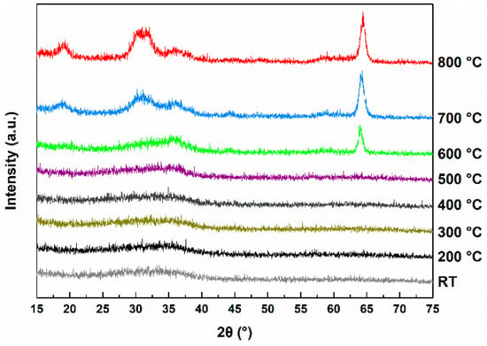
Figure 1.
XRD results at different post-annealing temperatures in the 100–800 °C range and without annealing (RT).
Figure 2 shows the XRD spectra as a function of the O2 flow ratio and post-annealing temperature. All samples annealed at temperatures above 600 °C exhibit β phase (403) peaks, with additional (-201), (002), and (400) peaks depending on the fabrication conditions. Figure 2a shows the XRD results of 600 °C annealed samples with varying Ar:O2 ratios. At 600 °C, other than the (403) peak, no distinct peaks can be observed. After the introduction of O2, there is a slight increase in the (400) and (002) peak positions; however, they are not clearly separated. In addition, increasing the O2 flow rate did not significantly change the diffraction peaks. Figure 2b shows XRD results of 700 °C annealed samples with varying Ar:O2 ratios. At 700 °C, the (403) peak is more intense than at 600 °C. Without O2 introduction (Ar only), as in the 600 °C condition, the (403) peak is the only prominent feature, but its intensity is noticeably stronger than at 600 °C. After the introduction of O2, distinct (-201), (400), and (002) peaks appear in addition to the (403) reflection. As the O2 flow rate increases, the intensity of the (403) peak gradually decreases. At 800 °C, the overall behavior is similar to that at 700 °C, but with two notable differences. First, after the O2 introduction, the (-201), (400), and (002) peaks exhibit lower intensities compared to the 700 °C case. Second, even without O2 flow, the (-201), (400), and (002) peaks are present, whereas at 700 °C these reflections appear distinct only after O2 introduction. In summary, the results indicate that both the O2 flow rate and the post-annealing temperature influence the structural characteristics of the Si-doped Ga2O3 thin films. Increasing the O2 flow rate reduces the intensity of the (403) reflection while enhancing the intensity of the other peaks. During deposition, the increasing O2 flow rate results in a decrease in the kinetic energy of the sputtered atoms, which leads to the low mobility of adatoms on the substrate. Low adatom mobility inhibits the migration of the adatom to its preferred position, leading to a change in the dominant peak [26]. In addition, an increase in the O2 flow rate results in a decrease in VO, providing sites for ion migration [27]. Increasing the post-annealing temperature leads to an overall increase in the peak intensities of the (-201), (400), (002), and (403) planes. This is likely because the higher temperature provides sufficient energy for the atoms in the film to migrate to the more stable lattice sites.
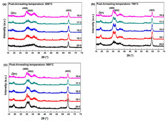
Figure 2.
XRD spectra at different Ar:O2 ratios and post-annealing temperatures: (a) 600 °C, (b) 700 °C, and (c) 800 °C.
Table 3 shows (403) peak information derived form XRD.

Table 3.
(403) peak information derived from XRD.
Because the (403) peak was distinctly present in all crystallized samples, Gaussian fitting was performed for the (403) peak. Based on this fitting, the full width at half maximum (FWHM) and the crystallite size were calculated. The crystallite size (D) was calculated using the Scherrer equation:
where K is the shape factor (0.9), λ is the X-ray wavelength (0.154 nm), β is the FWHM, and θ is the Bragg angle. Figure 3a–c shows that the FWHM and crystallite size vary with the post-annealing temperature and O2 flow rate. All samples have nanocrystalline structures with crystallite sizes ranging from 6.6 to 8.3 nm. The crystallite sizes exhibit different trends depending on the post-annealing temperature. For samples annealed at 600 °C and 800 °C, the crystallite size decreases as the O2 flow ratio increases from 0 to 2 sccm, then increases from 2 to 4 sccm. In contrast, for samples annealed at 700 °C, the crystallite size increases with the O2 flow ratio, except at 3 sccm. Figure 3d shows the strain induced by crystal imperfections and distortions in the samples as a function of the post-annealing temperature and O2 flow rate. Strain (ε) was calculated by following equation [28].
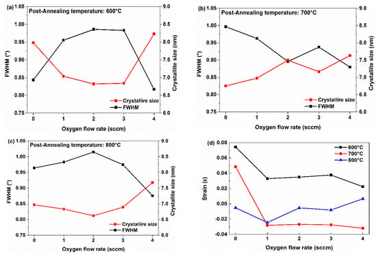
Figure 3.
FWHM and crystallite size calculated using XRD results at various temperatures: (a) 600 °C, (b) 700 °C, and (c) 800 °C. (d) Calculated strain.
Strain in thin films arises from a combination of multiple factors, including the film composition, crystal orientation, and lattice mismatch with the substrate [29,30]. Therefore, it is challenging to pinpoint the exact cause of strain based solely on XRD results. In Figure 3d, under the Ar-only condition (i.e., before O2 is introduced), the strain decreases as the annealing temperature increases, and the sample annealed at 800 °C shows a relatively small strain. This result aligns with the earlier explanation that a higher annealing temperature provides sufficient energy for atoms in the film to migrate to more stable sites, thereby reducing the overall strain. After post-annealing at 600 °C, the film appears to be in a tensile-strained state due to the presence of oxygen vacancies. Once O2 was introduced (from 0 to 1 sccm), the strain value decreased significantly. This implies that the reduction in VO at higher O2 flow rates helped relieve the tensile strain. This trend is attributed to the decreased VO formation energy with higher oxygen flow rates, leading to reduced VO in the samples [20,31]. At 700 °C, a similar trend is observed; however, the strain is negative, indicating compressive strain in the film. With the introduction of O2, the tensile strain transitioned to compressive strain. In other words, although annealing at 700 °C enables higher atomic mobility than that at 600 °C, it does not fully stabilize the crystal structure, making it an intermediate temperature at which compressive strain emerges in the film [32,33].
3.1.2. SEM Results
Figure 4 and Figure 5 shows the SEM results of Ar:O2 = 20:0 samples post-annealed at temperatures ranging from RT to 800 °C. Samples annealed at temperatures of 600 °C and above, where crystallization occurs, exhibit cracks. These cracks appear to be due to the lattice mismatch between β-Ga2O3 and Si. β-Ga2O3 has a monoclinic C2/m structure with lattice constants a = 12.23 Å, b = 3.04 Å, c = 5.8 Å, α = γ = 90°, and β = 103.7° [34], while Si has a cubic Fd3m structure with a lattice constant of 5.43 Å [35,36], leading to a significant lattice mismatch with β-Ga2O3. Therefore, at the crystallization temperature, lattice mismatch induces stress, leading to the formation of cracks. However, as the post-annealing temperature is increased, crack formation and propagation are inhibited, and this behavior is consistent with the results shown in Figure 3d. This is likely due to the sufficient mobility of atoms within the thin film during post-annealing, which induces crystallization and minimizes cracks.
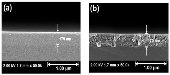
Figure 4.
SEM cross-sectional image of Ar:O2 = 20:0 samples: (a) without annealing, post-annealed at (b) 800 °C.
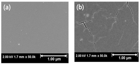
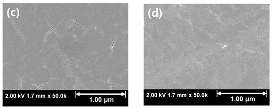
Figure 5.
SEM results for Ar:O2 = 20:0 samples with different post-annealing temperatures: (a) without annealing, annealed at (b) 600 °C, (c) 700 °C, and (d) 800 °C.
3.1.3. XPS Results
To elucidate the evolution of chemical states and defect structures in the Ga2O3 thin films, high-resolution XPS measurements were performed on samples subjected to different post-annealing temperatures. Because no depth profiling or sputter cleaning was applied, the reported XPS values correspond to the near-surface of the Ga2O3 films. XPS spectra were fitted in Origin using Gaussian peak functions
Figure 6 displays the O 1s and Ga 2p core-level spectra of the undoped Ga2O3, as-fabricated, and annealed samples (600, 700, 800 °C). After thermal annealing, the O/Ga atomic ratio exhibited a decreasing trend, which can be primarily attributed to the reduction of chemisorbed oxygen species on the film surface. These surface-adsorbed components (represented by the OIII peak at 531.96 eV) are known to desorb upon annealing, especially at elevated temperatures, thereby reducing the total oxygen signal detected by XPS. The O 1s peak was deconvoluted into three components to calculate oxygen vacancy concentration. Each peak was centered at 530.50 eV (OI), 531.03 eV (OII), and 531.96 eV (OIII), as shown in Figure 6 each component corresponds to a distinct chemical state of oxygen:
- •
- OI is attributed to lattice oxygen (O2−) bound in Ga–O–Ga networks.
- •
- OII is attributed to oxygen vacancies (VO), indicative of non-stoichiometric regions or local disorder.
- •
- OIII is attributed to chemisorbed species such as hydroxyl groups or adsorbed oxygen molecules on the film surface.
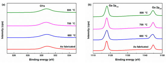
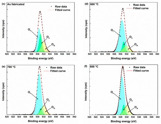
Figure 6.
XPS results (a) O 1s peak, (b) Ga 2p peak, peak deconvolution of (c) As fabricated sample, (d) 600 °C annealed sample, (e) 700 °C annealed sample, (f) 800 °C annealed sample.
The oxygen vacancy concentration at surface was evaluated using the area ratio OI/(OI + OII) obtained from the O 1s fitting results, as summarized in Table 4. This ratio serves as an indicator of the degree of lattice oxygen preservation versus vacancy-related oxygen species. With increasing annealing temperature VO concentration, drop from 41.54% in the as-fabricated sample to 9.05% after 700 °C annealing (Table 4). Notably, the 800 °C sample shows a slight increase in VO content (13.60%), possibly due to re-evaporation or the onset of defect formation from high temperature.

Table 4.
Summary of O/Ga Stoichiometry and VO Fraction from XPS.
3.2. Electrical Properties
Ga2O3 exhibits properties suitable for its use as an n-type material due to two main reasons. First, the 4s orbital of Ga has a wide spatial distribution, and its wave functions overlap with each other, providing a facile pathway for electron conduction. Second, because of the contraction of the Ga 3d orbitals, the Ga 4s orbitals have lower energies than those of other pre-transition metals. This results in a relatively high electron affinity, which facilitates n-type doping [37]. When Si is used as a dopant, Ga3+ ions are replaced by Si4+ ions, contributing to n-type conductivity [38].
Figure 7 shows the electrical properties of the Ga2O3 thin films determined from Hall effect measurements. All samples exhibited carrier concentrations above 1022 cm−3, mobilities exceeding 50 cm2/V·s, and resistivities on the order of 10−6 Ω·cm, demonstrating their high conductivity. Comparable values have also been reported in previous studies on sputtered Sn-doped Ga2O3 thin films at similar doping concentrations [39]. Figure 7a shows the carrier concentration as a function of the Ar:O2 ratio and post-annealing temperature. Several n-type oxide semiconductors obtain free electrons through oxygen vacancies [40,41]. However, in the case of gallium oxide, a comparison between the measured carrier concentration and the oxygen vacancy ratio calculated from XPS revealed that an increase in oxygen vacancy concentration does not correspond to an increase in carrier concentration. This different behavior of Ga2O3 toward oxygen vacancies is attributed to the fact that, in Ga2O3, oxygen vacancies act as deep donors rather than shallow donors. Numerous previous studies have reported that oxygen vacancies in Ga2O3 indeed exist as deep donors [25,42,43,44]. The carrier concentration exhibits a trend similar to that of the strain shown in Figure 3d. For samples post-annealed at 600 °C and 700 °C, the carrier concentration decreases with increasing O2 flow rate, with the most significant decrease occurring from 0 sccm to 1 sccm. Samples post-annealed at 800 °C maintain relatively low carrier concentrations, mirroring the trend seen in Figure 3d. It is considered that the strain relaxation or modification caused by thermal annealing may have affected the carrier concentration, possibly by altering the band structure, defect formation energy, or trap state distribution within the film. Figure 7b shows the variation in mobility as a function of the O2 flow ratio and post-annealing temperature. The characteristics of oxide semiconductors can be inferred from the mobility data. In the case of non-oxide semiconductors such as Si, the sp3 orbital characteristics result in increased disorder and significantly reduced mobility when the material is amorphous. However, for Ga2O3, the Ga 4s orbital, with its wide distribution and overlapping wave functions, provides a facile pathway for electrons that are not significantly affected by direction [45]. Therefore, Ga2O3 does not exhibit a substantial decrease in mobility. All fabricated samples exhibit high mobility above 50 cm2/Vs. Among the samples annealed in Ar, the one treated at 800 °C exhibited the highest mobility, which is likely due to the most significant crack mitigation. Figure 7c,d shows the variation in resistivity and sheet resistance as a function of the O2 flow ratio and post-annealing temperature. All the samples exhibited resistivities ranging from 9 × 10⁻⁷ to 1.3 × 10⁻⁶ Ω⋅cm and sheet resistance ranging from 0.05247 to 0.05412 Ω/sq. Although some changes in the resistivity and sheet resistance were observed depending on the conditions, the differences were not statistically significant.
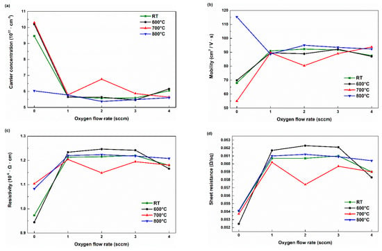
Figure 7.
Hall effect measurement results. (a) Carrier concentration, (b) mobility, (c) resistivity, (d) sheet resistance.
Table 5 shows electrical properties with different post-annealing temperatures.

Table 5.
Electrical properties with different post-annealing temperatures.
4. Conclusions
In this study, we investigated the effects of deposition conditions on the structural and electrical properties of β-Ga2O3 thin films. Our experimental results demonstrated that both the post-annealing temperature and the O2 flow rate during deposition significantly influence the properties of β-Ga2O3 thin films. The X-ray diffraction (XRD) analysis revealed that β-Ga2O3 films have distinct β-phase peaks at post-annealing temperatures of 600 °C and above, confirming the formation of the β-Ga2O3 phase. Structural characterization showed that increasing the O2 flow rate shifts the XRD peaks and changes in the strain, indicating variations in the crystallinity of the film and the density of oxygen vacancies. The oxygen vacancy ratio at the surface of the film was determined by XPS, while changes in crack formation with post-annealing temperature were examined using SEM. At 700 and 800 °C, the films exhibited relatively higher crystallinity. Under Ar-only annealing, increasing the post-anneal temperature reduced the (apparent) strain and alleviated crack formation. The results confirm that excellent electrical properties can be achieved by optimizing the deposition parameters. The β-Ga2O3 thin films exhibited carrier concentrations exceeding 5 × 1022 cm−3, mobilities in the range of 50 to 115 cm2/Vs, and resistivities around 1 × 10⁻⁶ Ω⋅cm. The observed electrical characteristics are closely linked to the structural characteristics of the films. The study underscores the interplay between the structural features and electrical performance of β-Ga2O3 thin films. Overall, our findings highlight that the properties of β-Ga2O3 thin films can be engineered through careful control of sputtering and post-treatment conditions. The ability to fine-tune these properties is crucial for the development of the next generation of high-performance electronic and optoelectronic devices. In future work, we plan to investigate the effect of varying Si doping concentrations on the electrical and structural properties of β-Ga2O3 thin films. While this study focused on the general trends in electrical properties as influenced by annealing and doping conditions, the underlying physical mechanisms—such as carrier scattering and trap-related effects—remain to be fully understood. Future work will involve temperature-dependent measurements and advanced spectroscopic analysis to provide a deeper understanding of these mechanisms. Comparison table of Ga2O3 films (Table 6).

Table 6.
Comparison table of Ga2O3.
Author Contributions
Conceptualization, H.K. and J.H.; methodology, H.K. and J.H.; validation, H.K. and J.H.; formal analysis, H.K., Y.K., N.M. and G.L.; investigation, H.K., Y.K., N.M. and G.L.; writing—original draft preparation, H.K.; writing—review and editing, J.H. All authors have read and agreed to the published version of the manuscript.
Funding
This work was supported by the Technology Innovation Program (RS-2023-00227306, Development of ultrasensitive DUV sensor for arc detection with high reliability in a natural light environment) funded by the Ministry of Trade, Industry & Energy (MOTIE, Republic of Korea) and the Gachon University Research Fund of 2023 (GCU-202400650001).
Institutional Review Board Statement
Not applicable.
Informed Consent Statement
Not applicable.
Data Availability Statement
Data are contained within the article.
Conflicts of Interest
Author Gonjae Lee was employed by the company HL Mando Corporation. The remaining authors declare that the research was conducted in the absence of any commercial or financial relationships that could be construed as a potential conflict of interest.
References
- Millan, J.; Godignon, P.; Perpiñà, X.; Pérez-Tomás, A.; Rebollo, J. A survey of wide bandgap power semiconductor devices. IEEE Trans. Power Electron. 2013, 29, 2155–2163. [Google Scholar] [CrossRef]
- Wan, X.; Xu, Y.; Guo, H.; Shehzad, K.; Ali, A.; Liu, Y.; Yang, J.; Dai, D.; Lin, C.T.; Liu, L.; et al. A self-powered high-performance graphene/silicon ultraviolet photodetector with ultra-shallow junction: Breaking the limit of silicon? NPJ 2D Mater. Appl. 2017, 1, 4. [Google Scholar] [CrossRef]
- Zhuo, Y.; Chen, Z.; Tu, W.; Ma, X.; Pei, Y.; Wang, G. β-Ga2O3 versus ε-Ga2O3: Control of the crystal phase composition of gallium oxide thin film prepared by metal-organic chemical vapor deposition. Appl. Surf. Sci. 2017, 420, 802–807. [Google Scholar] [CrossRef]
- Hou, Y.; Wu, L.; Wang, X.; Ding, Z.; Li, Z.; Fu, X. Photocatalytic performance of α-, β-, and γ-Ga2O3 for the destruction of volatile aromatic pollutants in air. J. Catal. 2007, 250, 12–18. [Google Scholar] [CrossRef]
- Irmscher, K.; Galazka, Z.; Pietsch, M.; Uecker, R.; Fornari, R. Electrical properties of β-Ga2O3 single crystals grown by the Czochralski method. J. Appl. Phys. 2011, 110, 063720. [Google Scholar] [CrossRef]
- Higashiwaki, M.; Sasaki, K.; Murakami, H.; Kumagai, Y.; Koukitu, A.; Kuramata, A.; Masui, T.; Yamakoshi, S. Recent progress in Ga2O3 power devices. Semicond. Sci. Technol. 2016, 31, 034001. [Google Scholar] [CrossRef]
- Galazka, Z.; Uecker, R.; Klimm, D.; Irmscher, K.; Naumann, M.; Pietsch, M.; Kwasniewski, A.; Bertram, R.; Ganschow, S.; Bickermann, M. Scaling-up of bulk β-Ga2O3 single crystals by the Czochralski method. ECS J. Solid State Sci. Technol. 2017, 6, Q3007–Q3011. [Google Scholar] [CrossRef]
- Aida, H.; Nishiguchi, K.; Takeda, H.; Aota, N.; Sunakawa, K.; Yaguchi, Y. Growth of β-Ga2O3 single crystals by the edge-defined, film fed growth method. Jpn. J. Appl. Phys. 2008, 47, 8506. [Google Scholar] [CrossRef]
- Yang, J.; Ren, F.; Tadjer, M.; Pearton, S.J.; Kuramata, A. 2300V reverse breakdown voltage Ga2O3 Schottky rectifiers. ECS J. Solid State Sci. Technol. 2018, 7, Q92–Q96. [Google Scholar] [CrossRef]
- Gong, H.H.; Yu, X.X.; Xu, Y.; Chen, X.H.; Kuang, Y.; Lv, Y.J.; Yang, Y.; Ren, F.F.; Feng, Z.H.; Gu, S.L.; et al. β-Ga2O3 vertical heterojunction barrier Schottky diodes terminated with p-NiO field limiting rings. Appl. Phys. Lett. 2021, 118, 202102. [Google Scholar] [CrossRef]
- Yen, C.-C.; Singh, A.K.; Wu, P.-W.; Chou, H.-Y.; Wuu, D.-S. Interface engineering in epitaxial growth of sputtered β-Ga2O3 films on Si substrates via TiN (111) buffer layer for Schottky barrier diodes. Mater. Today Adv. 2023, 17, 100348. [Google Scholar] [CrossRef]
- Guo, D.; Guo, Q.; Chen, Z.; Wu, Z.; Li, P.; Tang, W. Review of Ga2O3-based optoelectronic devices. Mater. Today Phys. 2019, 11, 100157. [Google Scholar] [CrossRef]
- Galazka, Z. β-Ga2O3 for wide-bandgap electronics and optoelectronics. Semicond. Sci. Technol. 2018, 33, 113001. [Google Scholar] [CrossRef]
- Nguyen, T.M.H.; Tran, M.H.; Bark, C.W. Growth of low-defect Si-doped Ga2O3 film on fluorine-doped tin oxide substrate for self-powered and high-performance ultraviolet photodetector. ACS Appl. Electron. Mater. 2023, 5, 6459–6468. [Google Scholar] [CrossRef]
- Zhang, Y.; Zhang, M.; Hu, W.; Hou, L.; Jiang, S.; Wang, Y.; Sun, J. Performance enhancement of solar-blind UV photodetector by doping silicon in β-Ga2O3 thin films prepared using radio frequency magnetron sputtering. Vacuum 2024, 227, 113399. [Google Scholar] [CrossRef]
- Wang, C.; Fan, W.H.; Cao, R.J.; Fan, H.C.; Xu, Y.H.; Kang, P.C.; Zhu, W.Z.; Kuo, H.-C.; Lien, S.-Y.; Zhu, W.-Z. Sputtered Sn-doped Ga2O3 films under balance controlled of energy supply and ion bombardment for solar-blind detection application. Vacuum 2024, 225, 113246. [Google Scholar] [CrossRef]
- Higashiwaki, M.; Murakami, H.; Kumagai, Y.; Kuramata, A. Current status of Ga2O3 power devices. Jpn. J. Appl. Phys. 2016, 55, 1202A1. [Google Scholar] [CrossRef]
- Li, K.-H.; Alfaraj, N.; Kang, C.H.; Braic, L.; Hedhili, M.N.; Guo, Z.; Ng, T.K.; Ooi, B.S. Deep-ultraviolet photodetection using single-crystalline β-Ga2O3/NiO heterojunctions. ACS Appl. Mater. Interfaces 2019, 11, 35095–35104. [Google Scholar] [CrossRef]
- Usseinov, A.; Platonenko, A.; Koishybayeva, Z.; Akilbekov, A.; Zdorovets, M.; Popov, A.I. Pair vacancy defects in β-Ga2O3 crystal: Ab initio study. Opt. Mater. X 2022, 16, 100200. [Google Scholar] [CrossRef]
- Dong, L.; Jia, R.; Xin, B.; Peng, B.; Zhang, Y. Effects of oxygen vacancies on the structural and optical properties of β-Ga2O3. Sci. Rep. 2017, 7, 40160. [Google Scholar] [CrossRef]
- Zhang, C.; Wu, X.; Xing, Y.; Zhou, L.; Zhou, H.; Li, S.; Xu, N. A first-principles study of hydrostatic strain engineering on the electronic properties of β-Ga2O3. Phys. B: Condens. Matter 2023, 660, 414851. [Google Scholar] [CrossRef]
- Zeng, H.; Ma, C.; Wu, M. High electron mobility in Si-doped two-dimensional β-Ga2O3 tuned using biaxial strain. Materials 2024, 17, 4008. [Google Scholar] [CrossRef]
- Chen, A.; Weigand, M.; Bi, Z.; Zhang, W.; Lü, X.; Dowden, P.; MacManus-Driscoll, J.L.; Wang, H.; Jia, Q. Evolution of microstructure, strain and physical properties in oxide nanocomposite films. Sci. Rep. 2014, 4, 5426. [Google Scholar] [CrossRef]
- Sun, Y.; Thompson, S.E.; Nishida, T. Physics of strain effects in semiconductors and metal–oxide–semiconductor field-effect transistors. J. Appl. Phys. 2007, 101, 104503. [Google Scholar] [CrossRef]
- Fu, B.; Jia, Z.; Mu, W.; Yin, Y.; Zhang, J.; Tao, X. A review of β-Ga2O3 single crystal defects, their effects on device performance and their formation mechanism. J. Semicond. 2019, 40, 011804. [Google Scholar] [CrossRef]
- Choi, C.G.; No, K.; Lee, W.J.; Kim, H.G.; Jung, S.O.; Lee, W.J.; Kim, W.S.; Kim, S.J.; Yoon, C. Effects of oxygen partial pressure on the microstructure and electrical properties of indium tin oxide film prepared by dc magnetron sputtering. Thin Solid Films 1995, 258, 274–278. [Google Scholar] [CrossRef]
- Reddy, A.M.; Reddy, A.S.; Lee, K.S.; Reddy, P.S. Effect of oxygen partial pressure on the structural, optical and electrical properties of sputtered NiO films. Ceram. Int. 2011, 37, 2837–2843. [Google Scholar] [CrossRef]
- Mote, V.; Purushotham, Y.; Dole, B. Williamson-Hall analysis in estimation of lattice strain in nanometer-sized ZnO particles. J. Theor. Appl. Phys. 2012, 6, 6. [Google Scholar] [CrossRef]
- Röll, K. Analysis of stress and strain distribution in thin films and substrates. J. Appl. Phys. 1976, 47, 3224–3229. [Google Scholar] [CrossRef]
- Janssen, G.C.A.M. Stress and strain in polycrystalline thin films. Thin Solid Films 2007, 515, 6654–6664. [Google Scholar] [CrossRef]
- Qu, L.; Ji, J.; Liu, X.; Shao, Z.; Cui, M.; Zhang, Y.; Fu, Z.; Huang, Y.; Yang, G.; Feng, W. Oxygen-vacancy-dependent high-performance α-Ga2O3 nanorods photoelectrochemical deep UV photodetectors. Nanotechnology 2023, 34, 225203. [Google Scholar] [CrossRef]
- An, Y.; Dai, L.; Wu, Y.; Wu, B.; Zhao, Y.; Liu, T.; Hao, H.; Li, Z.; Niu, G.; Zhang, J.; et al. Epitaxial growth of β-Ga2O3 thin films on Ga2O3 and Al2O3 substrates by using pulsed laser deposition. J. Adv. Dielect. 2019, 9, 1950032. [Google Scholar] [CrossRef]
- Kyrtsos, A.; Matsubara, M.; Bellotti, E. Migration mechanisms and diffusion barriers of vacancies in Ga2O3. Phys. Rev. B 2017, 95, 245202. [Google Scholar] [CrossRef]
- Geller, S. Crystal structure of β-Ga2O3. J. Chem. Phys. 1960, 33, 676–684. [Google Scholar] [CrossRef]
- Pishkenari, H.N.; Rezaei, S. Characterization of silicon surface elastic constants based on different interatomic potentials. Thin Solid Films 2017, 626, 104–109. [Google Scholar] [CrossRef]
- Aliev, R.; Rashidov, B.; Mirzaalimov, A.; Mirzaalimov, N.; Aliev, S.; Gulomova, I.; Gulomov, J. The effect of uniaxial mechanical stress on electronic and dynamic properties of silicon. Dig. J. Nanomater. Biostruct. 2024, 19, 1243–1253. [Google Scholar] [CrossRef]
- Zhang, J.; Shi, J.; Qi, D.C.; Chen, L.; Zhang, K.H.L. Recent progress on the electronic structure, defect, and doping properties of Ga2O3. APL Mater. 2020, 8, 020906. [Google Scholar] [CrossRef]
- Varley, J.B.; Weber, J.R.; Janotti, A.; Van de Walle, C.G. Oxygen vacancies and donor impurities in β-Ga2O3. Appl. Phys. Lett. 2010, 97, 142106. [Google Scholar] [CrossRef]
- Kim, J.; Kubota, Y.; Matsushita, N.; Lee, G.; Kyoung, S.; Kim, K.; Hong, J. Effect of Post-Annealing and Oxygen on the Properties of Sn-Doped β-Ga2O3 Thin Film. Trans. Electr. Electron. Mater. 2025, 26, 746–756. [Google Scholar] [CrossRef]
- Liu, L.; Mei, Z.; Tang, A.; Azarov, A.; Kuznetsov, A.; Xue, Q.K.; Du, X. Oxygen Vacancies: The Origin of n-Type Conductivity in ZnO. Phys. Rev. B 2016, 93, 235305. [Google Scholar] [CrossRef]
- Madkhali, O. A Review of Novel Methods to Improve the Optical and Electrical Properties of n-Type and p-Type Sulphides and Oxides: Leading the Frontiers of Semiconductor Technology. Phys. Scr. 2024, 99, 022004. [Google Scholar] [CrossRef]
- McCluskey, M.D. Point Defects in Ga2O3. J. Appl. Phys. 2020, 127, 101101. [Google Scholar] [CrossRef]
- Polyakov, A.Y.; Nikolaev, V.I.; Yakimov, E.B.; Ren, F.; Pearton, S.J.; Kim, J. Deep Level Defect States in β-, α-, and ɛ-Ga2O3 Crystals and Films: Impact on Device Performance. J. Vac. Sci. Technol. A 2022, 40, 020804. [Google Scholar] [CrossRef]
- Wang, Z.; Chen, X.; Ren, F.F.; Gu, S.; Ye, J. Deep-Level Defects in Gallium Oxide. J. Phys. D Appl. Phys. 2020, 54, 043002. [Google Scholar] [CrossRef]
- Hosono, H. Ionic amorphous oxide semiconductors: Material design, carrier transport, and device application. J. Non-Cryst. Solids 2006, 352, 851–858. [Google Scholar] [CrossRef]
- Leedy, K.D.; Chabak, K.D.; Vasilyev, V.; Look, D.C.; Boeckl, J.J.; Brown, J.L.; Jessen, G.H. Highly conductive homoepitaxial Si-doped Ga2O3 films on (010) β-Ga2O3 by pulsed laser deposition. Appl. Phys. Lett. 2017, 111, 012103. [Google Scholar] [CrossRef]
- Zhang, F.; Arita, M.; Wang, X.; Chen, Z.; Saito, K.; Tanaka, T.; Guo, Q. Toward controlling the carrier density of Si-doped Ga2O3 films by pulsed laser deposition. Appl. Phys. Lett. 2016, 109, 102105. [Google Scholar] [CrossRef]
- Juárez-Amador, L.I.; Galván-Arellano, M.; Andraca-Adame, J.A.; Romero-Paredes, G.; Kennedy-Magos, A.; Peña-Sierra, R. Electrical, optical and structural characteristics of gallium oxide thin films deposited by RF-sputtering. J. Mater. Sci. Mater. Electron. 2018, 29, 15726–15731. [Google Scholar] [CrossRef]
- Mandal, P.; Roy, S.; Singh, U.P. Optimization of RF sputtering parameters for improving the optical and electrical properties of β-gallium oxide thin films. Bull. Mater. Sci. 2023, 46, 64. [Google Scholar] [CrossRef]
Disclaimer/Publisher’s Note: The statements, opinions and data contained in all publications are solely those of the individual author(s) and contributor(s) and not of MDPI and/or the editor(s). MDPI and/or the editor(s) disclaim responsibility for any injury to people or property resulting from any ideas, methods, instructions or products referred to in the content. |
© 2025 by the authors. Licensee MDPI, Basel, Switzerland. This article is an open access article distributed under the terms and conditions of the Creative Commons Attribution (CC BY) license (https://creativecommons.org/licenses/by/4.0/).