Abstract
Transition metal dichalcogenides (TMDC) have been considered promising electronic materials in recent years. Annealing and chemical doping are two core processes used in manufacturing electronic devices to modify properties and improve device performance, where annealing enhances crystal quality, reduces defects, and enhances carrier mobility, while chemical doping modifies conductivity and introduces new energy levels within the bandgap. In this study, we investigate the annealing effects of various types of dopants, time, and ambient conditions on the diverse material properties of TMDCs, including crystal structure quality, defect density, carrier mobility, electronic properties, and energy levels within the bandgap.
1. Introduction
Transition metal dichalcogenides (TMDCs) have received considerable attention over the years. TMDC is a type of two-dimensional (2D) material similar to graphene [1,2,3,4], but rather than a single layer of carbon atoms in graphene, it consists of a single layer of transition metal atoms including molybdenum (Mo) [5,6,7,8], tungsten (W) [9,10,11], and platinum (Pt) [12,13,14,15] sandwiched between two layers of chalcogen. An atom includes sulfur (S) [16,17,18,19], selenium (Se) [20,21,22,23], and tellurium (Te) [24,25,26]. TMDCs offer various interesting properties, such as high electron mobility, strong optical-matter interactions, and mechanical flexibility. These properties make them promising candidates for a variety of applications in fields such as thin-film transistors [27,28,29,30], photosensors [31,32,33], gas detectors [34,35,36], neuromorphic devices [37,38,39,40], biosensors [41,42,43,44] and energy harvesting devices [45,46,47]. In recent years, significant efforts have been made to develop new methods for synthesizing TMDC and to explore its properties in more detail. This allowed a better understanding of the fundamental physics of TMDCs and opened new avenues for their use in a variety of applications.
Annealing is a simple yet effective method for controlling the properties of TMDCs [48,49,50,51]. This process involves heating the material to a specific temperature for a defined duration and slowly cooling it in a controlled environment. The outcome of annealing on TMDCs can be influenced by various factors, such as the annealing temperature [52,53,54,55], duration [56,57,58], and atmosphere [59,60,61,62]. One of the most significant advantages of annealing on TMDCs is the elimination of defects and impurities that can degrade their electronic and optical properties, thus enhancing device performance [63,64,65].
In addition, annealing can also affect the electronic and optical properties of TMDCs [66,67,68,69]. For instance, it can cause shifts in the bandgap energy [70,71], making it useful in optoelectronic devices [72,73,74]. Furthermore, annealing can improve electron mobility [75,76,77] and carrier concentration [78,79] and enhance electrical conductivity [80,81,82]. The effect of annealing on TMDC is also dependent on the atmosphere in which the process is carried out. For example, annealing in a controlled atmosphere can create sulfur or selenium voids that can alter the electronic and optical properties of the material [83,84]. Annealing in an oxidizing atmosphere can also generate an oxide layer on the material surface, which can impact electronic and optical properties [85,86,87].
In addition, the chemical doping method is considered to improve electrical properties of TMDC while minimizing lattice structure damage. Chemical dopant could modulate the distance between the Fermi level and the conduction band or valence band [88]. Therefore, doping the TMDC with an appropriate dopant reduces the height of the Schottky barrier and enhances the carrier density [89].
Here, we present the effects of annealing and chemical doping on the various TMDC—Based transistors. This review provides details on the TMDC transistor’s annealing process in different environments, including air, nitrogen, and vacuum. Additionally, we discuss changes in the electrical characteristics of TMDC transistors resulting from organic dopants such as dielectrics and SAM. Finally, we examine the potential for performance enhancement in electronic engineering based on TMDC materials and suggest future directions for research.
2. Synthesis of Transition Metal Dichalcogenides
TMDC materials possess unique electronic and optical properties, valuable for electronic and optoelectronic devices. High-quality TMDC monolayers or few-layer structures are crucial for these applications. Mechanical exfoliation, using Scotch tape or metal assistance, provides a simple and cost-effective method for obtaining single layers from bulk crystals [90,91,92]. Meanwhile, chemical vapor deposition (CVD) allows controlled growth of large-area monolayers with desired properties on different substrates [93,94]. Liquid-phase exfoliation is a low-cost, scalable method for mass production but faces challenges in obtaining single atomic layers with specific structures [95,96]. Ongoing research aims to optimize exfoliation processes for addressing this issue.
3. The Fundamental Processes Occurring during Annealing in the TMDC
Annealing is utilized in shaping the crystal structure, crystallinity, and defects of TMDC, exerting crucial control over the material’s electrical and optical properties [97,98,99,100,101]. Different from graphene, monolayer TMDC consists of sandwich structures with chalcogen atoms forming upper and lower layers and a transition metal ion plane in between. These TMDCs can be classified into 2H and 1T phases, each with distinct properties. The 2H phase exhibits excellent optical emission characteristics but limited electrical catalytic properties, while the 1T phase demonstrates superior catalytic properties but lacks light-absorbing capabilities due to its metallic nature. Through annealing, transitions between these crystal structures can be induced, enabling precise control to achieve desired characteristics.
Moreover, annealing influences the growth of crystalline domains, impacting crystal boundaries and thereby regulating charge transport and electrical properties. Additionally, the annealing process reduces defects and imperfections, leading to enhanced electrical and optical properties. In intentionally doped TMDC, annealing facilitates the diffusion of dopants into the crystal lattice, resulting in improved electronic properties and the ability to tailor specific functionalities. The outcomes of these annealing effects depend on various conditions such as temperature, time, and environment, allowing for fine tuning of TMDC properties for diverse applications.
4. Annealing Effects of TMDC—Based Transistors
4.1. Annealing Effects of MoS2—Based Transistors
The n-doping effect of molybdenum disulfide (MoS2) FET was demonstrated through a simple annealing process. This study performed annealing for 2 h in a nitrogen atmosphere [102]. Figure 1a shows the transfer curve of a MoS2 FET with the effect of vacuum annealing, where the pristine MoS2 FET exhibits a low on/off-current ratio of 100 A/A due to its high off current of 10−5 A. The off current of the MoS2 FET annealed at 200 °C was below 10−11 A at negative gate voltage, indicating the n-type doping effect. The off current of the MoS2 FET annealed at 300 °C shows a slight increase compared to that at 200 °C. The decrease in the off current is due to the rearranged surface of the MoS2 channel and the removal of residual material through heat. On the other hand, increasing the annealing temperature to 400 °C resulted in a decrease in the on current and an increase in the off current, with a drain current of 10−5 A and an ambiguous boundary between the on/off currents. The high off current of the MoS2 FET is attributed to the phase transformation to Mo2S5 caused by high-temperature energy. Moreover, when the electrical characteristics are measured in atmospheric environments, the adsorption of water and oxygen molecules on the annealing-treated MoS2 channel region leads to an increase in the off current. Figure 1b shows the on/off current of the MoS2 FET as a function of annealing temperature. The on current continues to decrease as the annealing temperature current becomes the initial drain current value. Figure 1c shows the extracted charge carrier mobility of the MoS2 FET with annealing temperature. The electron mobility of a pristine MoS2 FET is 8.5 cm2 V−1 s−1, but the highest electron mobility of 20.7 cm2 V−1 s−1 appears at the lowest off-state current under annealing conditions of 200 °C, and as the annealing temperature increases above 200 °C, the electron mobility decreases.
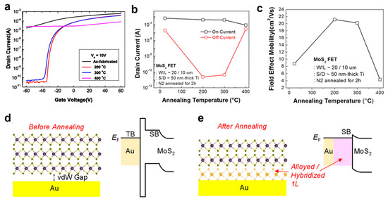
Figure 1.
(a) Transfer curve of MoS2 FET according to annealing temperature; (b) The plotted on- and off-current values of MoS2 FET; (c) The extracted field effect mobility of MoS2 FET according to annealing temperature (adapted from [102] with permission from the Springer Science and Business Media); Band structure of the Au contact electrode and MoS2 channel (d) before annealing and, (e) after annealing (adapted from [103] with permission from the AIP Publishing LLC).
As another example, the induced n-doping effect in MoS2 FET through a vacuum annealing process was reported by Islam et al. [103]. The pristine MoS2 FET was mounted on a furnace and annealed at 250 °C under a vacuum of 15 mTorr for 1 h. The contact and channel resistances of the pristine MoS2 FET were 4 MΩ and 112 kΩ, respectively, while the annealed MoS2 FET had a contact resistance of 2 kΩ and a channel resistance of 171 kΩ. Figure 1d shows the band structure of the pristine MoS2 FET. A vacuum annealing process reduced the contact and channel resistances of the device, despite the presence of a high contact resistance caused by the tunneling barrier between the Au contact electrode and the MoS2 channel due to the Van der Waals gap. The vacuum-annealed interface between the Au contact electrode and MoS2 channel is alloyed, eliminating the Van der Waals gap and tunneling barrier (Figure 1e). Additionally, the alloyed Au contact electrode and MoS2 channel had reduced work function, leading to a decreased Schottky barrier, and consequently lowering the contact resistance. This vacuum annealing process increases the mobility of MoS2 FET from 0.1 to 8 cm2 V−1 s−1 and enhances the on/off ratio 10 fold.
4.2. Annealing Effects of MoTe2—Based Transistors
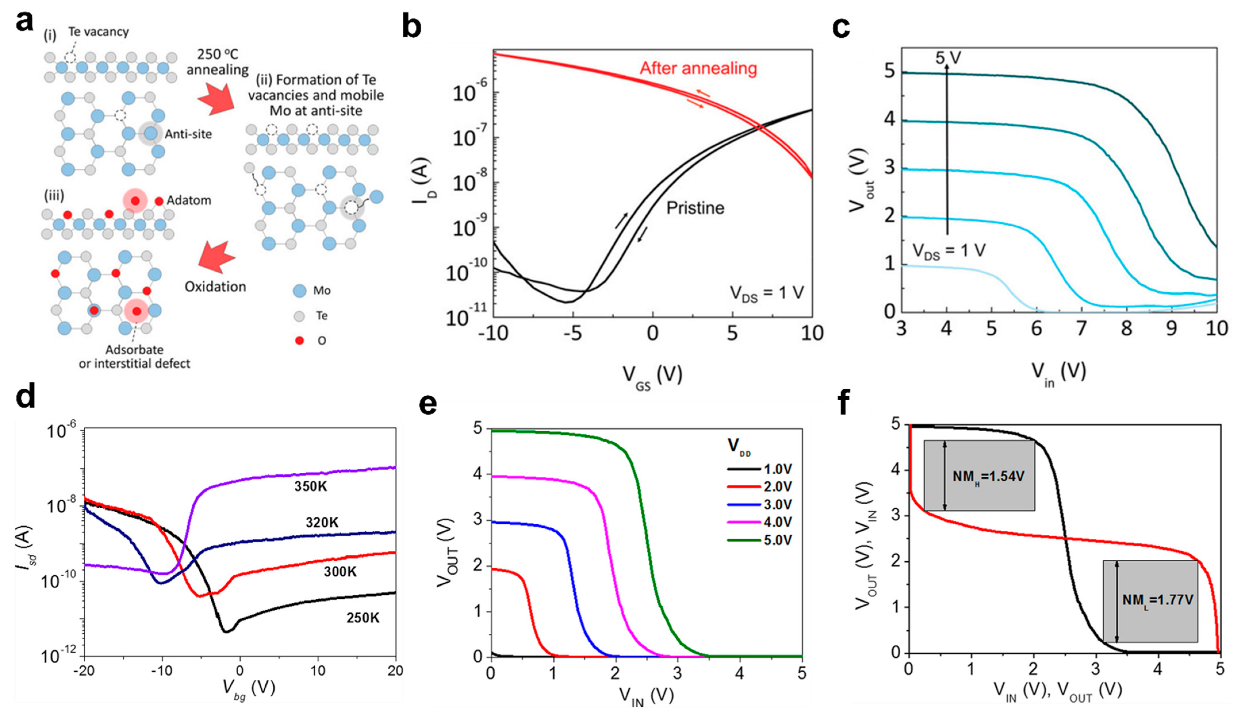
To change the electrical characteristics of n-type molybdenum ditelluride (MoTe2) FETs, a p-type doping method through an annealing process was reported [104]. This annealing process led to a MoTe2—Based complementary metal-oxide semiconductor (CMOS) inverter using a p-type MoTe2 FET with an annealing process and an n-type MoTe2 FET with electron beam irradiation. To manufacture a p-type MoTe2 FET, a rapid thermal annealing (RTA) process was performed at 250 °C for 3 h. Figure 2a shows the molecular structure of oxidized MoTe2 resulting from the annealing process. MoTe2 has bonds such as Te vacancy and antisites. Upon high-temperature annealing treatment, the Te vacancy was increased and induced the absorption of oxygen molecules. As a result, oxygen molecules with high electronegativity are adsorbed onto the Te vacancy in oxidized MoTe2, acting as electron acceptors and inducing a p-type doping effect on MoTe2 FET. Figure 2b shows the electrical properties of the pristine MoTe2 FET and the annealed MoTe2 FET. After the annealing process, the MoTe2 FET enhanced p-type behavior, and the hysteresis was reduced. Also, the doping effect of p-type MoTe2 FET induced by high-temperature annealing lasted for 2 weeks. Figure 2c shows the voltage transfer characteristics (VTC) of a CMOS inverter implemented using an annealed treated p-type MoTe2 FET and an n-type MoTe2 FET fabricated by electron beam irradiation. The CMOS inverter exhibits full-swing operation over a drain voltage range of 1 V to 5 V.

Figure 2.
(a) Schematic of MoTe2 structure with annealing and oxidation; (b) Transfer curve of pristine MoTe2 FET and annealed MoTe2 FET; (c) Voltage transfer characteristics of MoTe2 based CMOS inverter (VDS was applied from 1 V to 5 V at 1 V interval). (adapted from [104] with permission from the John Wiley and Sons); (d) Transfer curve of MoTe2 FET according to vacuum annealing temperature; (e) Voltage transfer characteristics of MoTe2 inverter; (f) Voltage transfer characteristics (black lines) and their mirrors (red lines) of MoTe2 inverter at VDD = 5 V (adapted from [105] with permission from the Springer Science and Business Media).
When oxygen or water molecules in the air are adsorbed onto the MoTe2 channel, it operates as a p-type transistor. However, the vacuum annealing process removes the adsorbed molecules from the MoTe2 channel. Consequently, Te vacancies are generated in the MoTe2 channel due to the removed adsorbates, resulting in the acquisition of n-type conductivity [105]. Figure 2d shows the transfer curves of the n-type MoTe2 FET through the vacuum annealing process. The pristine MoTe2 FET operates as a p-type due to the incomplete removal of adsorbates from the MoTe2 channel. In contrast, when the temperature is increased to 76.85 °C, the drain current at both positive and negative gate voltages decreases and increases, respectively. The n-type MoTe2 FET has on/off ratio of 3.8 × 10² A/A, an S.S of 1.1 V/dec, and electron mobility of 2 cm2 V−1 s−1. In addition, the inverter was demonstrated using unipolar p-type and n-type MoTe2 FETs. Figure 2e shows the VTC characteristics of the MoTe2 inverter. The transition voltage was half of VDD due to the transfer curve of p- and n-type of MoTe2 FET being symmetrical. Figure 2f shows the noise margin and VTC curve of the MoTe2 inverter when VDD is 5 V. The low-level noise margin (NML) is 1.54 V, while the high-level noise margin (NMH) is 1.77 V.
4.3. Annealing Effects of WSe2—Based Transistors
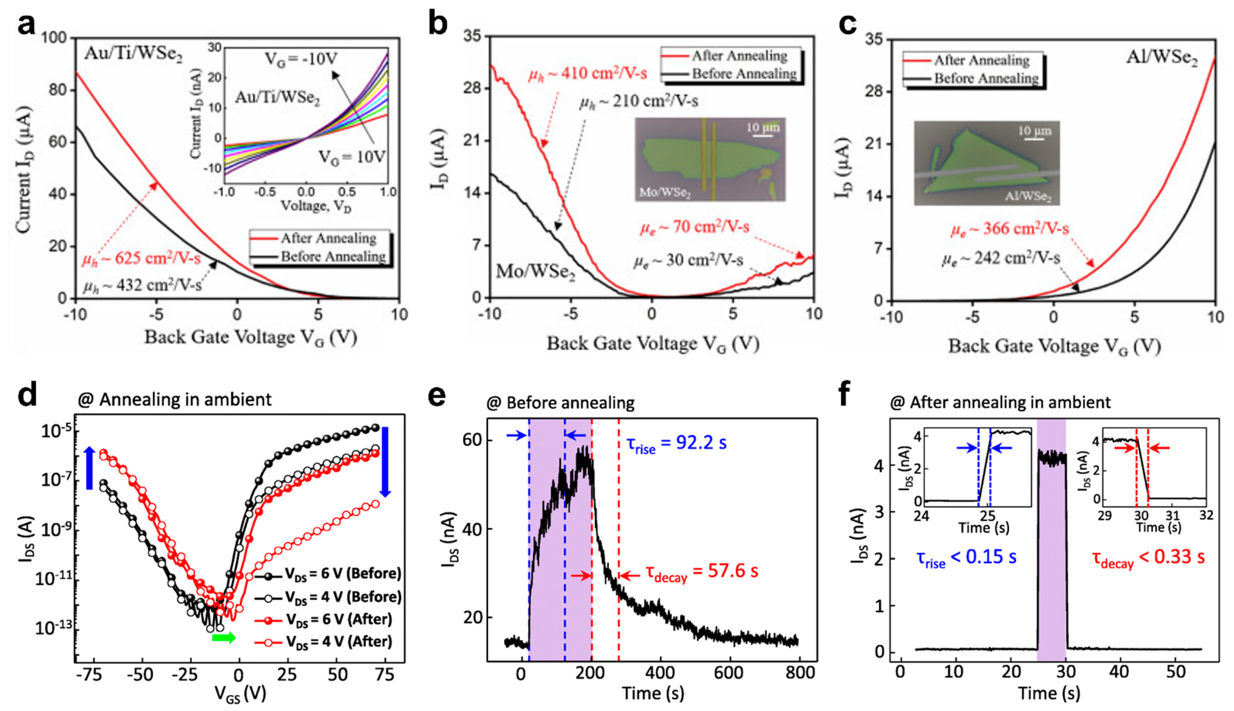
The work function of the electrode and the subsequent annealing process changed the electrical characteristics of the tungsten diselenide (WSe2) FET. Bandyopadhyay et al. fabricated WSe2 FET using various metal electrodes with different work functions, such as gold (Au, ϕm = ~5.4 eV), molybdenum (Mo, ϕm = ~4.53 eV), and aluminum (Al, ϕm = ~4.08 eV) [106]. The WSe2 FET with metal electrodes of different work functions operates as both n-type and p-type transistors. Furthermore, the field effect mobility and on current were increased by 300 °C vacuum, annealing for 3 h. Figure 3a shows the transfer curve of a WSe2 FET with Au/Ti electrodes. The hole mobility of the pristine Au/Ti/ WSe2 FET was 432 cm2 V−1 s−1, but it increased by 150% to 625 cm2 V−1 s−1 after the annealing process with enhancing p-type operation. This indicates the interface properties between the WSe2 channel and gate dielectric are enhanced by annealing effects. Figure 3b shows the transfer curve of WSe2 FETs with Mo electrodes. The pristine Mo/WSe2 FET had ambipolar behavior with p-type dominance, and the hole and electron mobilities were 210 and 30 cm2 V−1 s−1, respectively. The additional annealing process further improved the ambipolar conduction of the Mo/WSe2 FET. The annealed Mo/WSe2 FET had a hole mobility of 410 cm2 V−1 s−1 and an electron mobility of 70 cm2 V−1 s−1. On the other hand, WSe2 FET with Al electrodes resulted in an n-type operation (Figure 3c). The electron mobility of the Al/WSe2 FET before and after annealing was 242 and 366 cm2 V−1 s−1, respectively. In summary, the conductivity of WSe2 FETs with dissimilar electrode work functions can be controlled as either n-type or p-type, and additional vacuum annealing shows the annealing effects of the device, inducing high mobility.
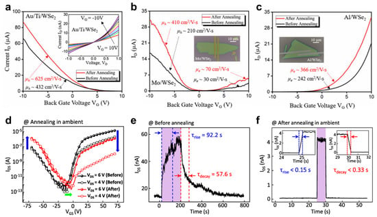
Figure 3.
Transfer curve of WSe2 FETs with various metal electrodes such as (a) gold/titanium, (b) molybdenum, and (c) aluminum (adapted from [106] with permission from the Elsevier B.V.); (d) Transfer curve of pristine WSe2 FET and annealed WSe2 FET under air ambient; Photo-switching behavior of (e) pristine WSe2 FET and, (f) WSe2 FET annealing at air ambient (adapted from [107] with permission from the Springer Science and Business Media).
The annealing process performed in ambient air causes the formation of an oxide layer (WO3) due to the interaction between the WSe2 surface and oxygen molecules. The p-doping effect on ambipolar WSe2 FET using an annealing process in ambient environment was observed [107]. The work function of WO3 (~6.7 eV) formed on the WSe2 surface under this condition is lower than that of WSe2 (~4.4 eV), resulting in a WSe2 FET operating as a p-type transistor. Figure 3d shows the modified transfer curves of the ambipolar WSe2 FET after annealing in air ambient. The WSe2 FET was annealed at 200 °C on a hot plate for 1 h. After annealing, the n-type current (VG = 70 V) of the ambipolar WSe2 FET decreased at all drain voltages (VD = 4 V, 6 V), and the p-type current increased (VG = −70 V). Also, the hole and electron mobility before annealing are 0.13 and 5.5 cm2 V−1 s−1, respectively. In contrast, when WSe2 FET was annealed, the extracted hole mobility increased up to 1.3 cm2 V−1 s−1, while the electron mobility decreased to 0.69 cm2 V−1 s−1. Figure 3e,f show the photo-switching characteristics of the pristine WSe2 FET and the annealed WSe2 FET. A 405 nm laser with a power density of 11 mW/cm2 was applied. In the switching operation, the rise time and decay time of the pristine WSe2 FET were 92.3 s and 57.6 s, respectively. In contrast, the rise time of the annealed WSe2 FET decreased significantly by 610 times to 0.15 s. Also, the decay time decreased to less than 0.33 s with a 170 times difference. The improved optical switching behavior is attributed to the lattice mismatch between WSe2 and WO3 generated by the proposed annealing process, and the recombination of photo-generated electron-hole pairs is facilitated by the trap regions resulting from the lattice mismatch.
4.4. Annealing Effects of WS2—Based Transistors
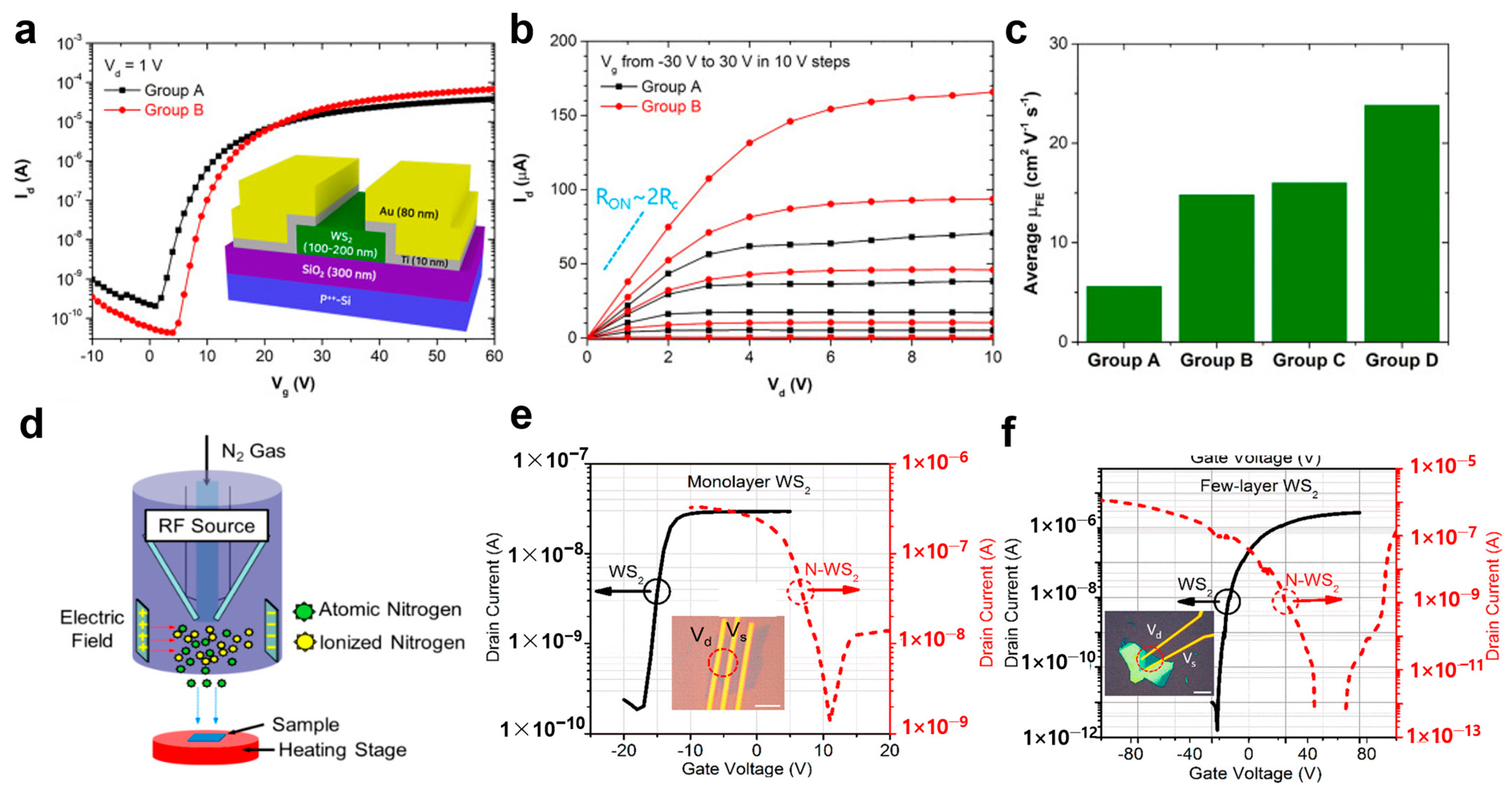
The n-type behavior of multilayer tungsten disulfide (WS2) FET through a double annealing process, performed both before and after electrode deposition, was demonstrated by Ji et al. in 2022 [108]. The first annealing process was carried out for 2 h at 200 °C on a WS2 transferred substrate mounted in a vacuum tube furnace. The first annealing process removed the organic residue and improved the WS2/electrode interface by desorbing the surface adsorbent. The second annealing process was also performed in a vacuum tube furnace at 200 °C after electrode deposition. Figure 4a shows the transfer curve of pristine WS2 FET (Group A) and annealed after electrode deposition WS2 FET (Group B). The on/off ratio and field effect mobility of pristine WS2 FET were 1.9 × 10⁵ A/A and 11.1 cm2 V−1 s−1, respectively. In contrast, the WS2 FET performed by annealing process after electrode deposition had 1.6 × 10⁶ A/A of on/off ratio and 20.8 cm2 V−1 s−1 of field effect mobility. Also, the output curves of WS2 FET from groups A and B showed a decrease in contact resistance from ~6.7 × 10² kΩ∙μm to ~3.8 × 10² kΩ∙μm (Figure 4b). Statistical analysis of the field effect mobility for 50 WS2 FET in each group was also performed (Figure 4c). Group C performed with an annealing process after the WS2 flake transfer, while Group D comprised WS2 FETs that carried out a double annealing process. The average field effect mobility of pristine WS2 FET was the lowest at 5.6 cm2 V−1 s−1. The average field effect mobility with the first and second annealing processes was 14.8 and 16.0 cm2 V−1 s−1, respectively. In contrast, the average field effect mobility of WS2 FET performed double annealing process was the highest at 23.8 cm2 V−1 s−1. Thus, the mobility and contact resistance of the WS2 FET were improved through double annealing processing.

Figure 4.
Electrical characteristics comparison between the pristine WS2 FET and the annealed after electrode deposition WS2 FET using (a) Transfer curves and, (b) Output curves; (c) Statistical analysis of 50 WS2 FET with A to D groups (adapted from [108] with permission from the Elsevier B.V.); (d) 3D schematic of the WS2 nitrogen substitutional doping and annealing process; Transfer curves of pristine WS2 FET and nitrogen doping WS2 FET with (e) monolayer WS2 and, (f) few layer WS2 (adapted from [109] with permission from the American Chemical Society).
WS2 typically exhibits n-type conductivity in both exfoliated flakes and chemical vapor deposition (CVD) growth. Nitrogen substitution doping and annealing manifest p-doping effects on WS2 FETs through Fermi-level pinning, which is a technological achievement for implementing TMDC—Based CMOS FETs [109]. The WS2 films were grown using radio frequency (RF) magnetron sputtering, followed by nitrogen annealing at 300 °C under a pressure of 7.0 × 10⁻⁵ mbar. The nitrogen radicals composed of ionized nitrogen and atomic nitrogen were effused into WS2 samples mounted on the main chamber and created W–N bonds (Figure 4d). The W–N bonds created by substituting S atoms in WS2 with N atoms result in an acceptor level 0.24 eV lower than the conduction band edge of WS2, enabling p-type doping. Figure 4e shows the transfer curves of a monolayer n-type WS2 and a p-type WS2 FET after nitrogen treatment. The hole mobility and the threshold voltage of the n-type WS2 FET are 0.53 cm2 V−1 s−1 and 9 V, respectively. However, a p-type WS2 FET with nitrogen substitutional doping had 1.70 cm2 V−1 s−1 of hole mobility and −12 V of the threshold voltage. Similarly, nitrogen annealing also enables the p-type operation of multilayer WS2 FET (Figure 4f). The p-type doping effect of WS2 FET by nitrogen substitutional doping and the annealing process is due to Fermi-level pinning.
The electrical properties of TMDCs can be changed depending on the annealing temperature and the environment (Table 1). Thus, depending on the intended application, the appropriate type of TMDC should be selected, and the required electrical properties should be achieved with suitable processing methods. Table 1 summarizes the characteristics of TMDC—Based transistors depending on the annealing conditions.

Table 1.
The influence of annealing on the characteristics of TMDC—Based transistors.
5. Annealing and Chemical Doping Effects in TMDC—Based Transistors
5.1. Annealing and Chemical Doping Effects in MoS2—Based Transistors
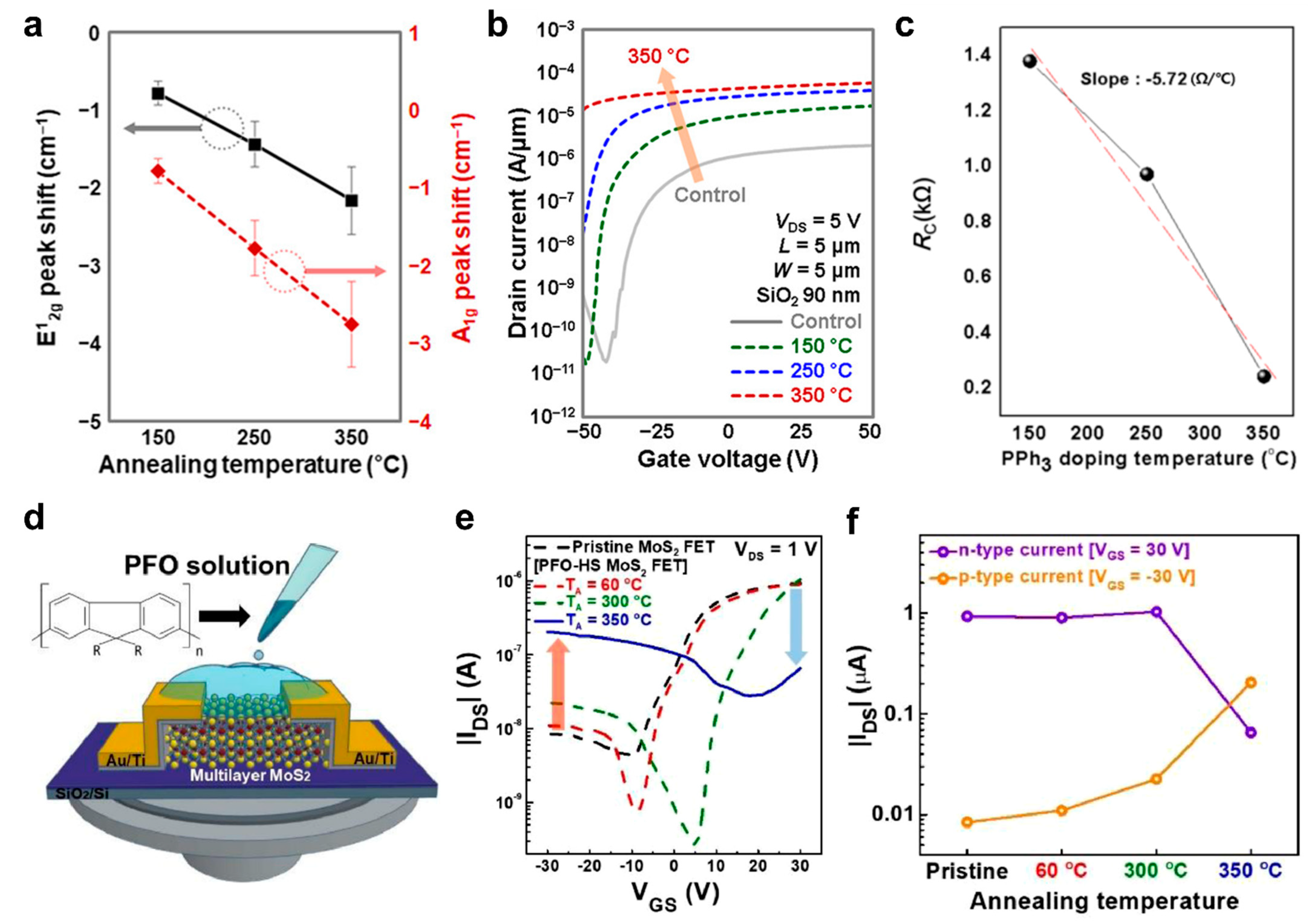
The formation of a triphenylphosphine (PPh3) layer can be controlled by annealing temperature. The use of PPh3 provided the n-doping effect of MoS2 FET through continuous annealing at three different temperatures (150, 250, and 350 °C) after spin coating a 7.5 wt% PPh3 solution on the surface of transistor [110]. The coated phosphorus atoms of PPh3 transfer electrons to the MoS2 surface, inducing an n-doping effect. Also, the PPh3 layers increase the number of electrons moving to the MoS2 channel as the annealing temperature increases. Raman spectroscopy was performed to analyze the n-doping effect of MoS2. Figure 5a shows the redshift values of the E2g1 peak and the A1g peak of MoS2 according to the annealing temperature. At 150 °C annealing conditions, both the E2g1 peak and the A1g peak are redshifted by −0.78 cm−1. As the annealing temperature increases to 350 °C, the E2g1 peak and the A1g peak are redshifted by −2.16 cm−1 and −2.75 cm−1, respectively. This indicates that PPh3 formation at higher annealing temperatures results in an enhanced n-doping effect. Figure 5b shows the transfer curve of pristine MoS2 and PPh3-doped MoS2 FET with annealed from 150 °C to 350 °C. As the annealing temperature increases, the on current of the PPh3-doped MoS2 FET increases, and the threshold voltage shifts towards negative gate voltages. Furthermore, the energy barrier height of PPh3 decreases, resulting in a decrease in contact resistance from 2.82 kΩ to 0.24 kΩ (Figure 5c). In addition, the on/off-current ratio and carrier mobility of PPh3-doped MoS2 FET improved to 8.70 × 10⁵ A/A and 241 cm2 V−1 s−1, respectively, from their initial values of 8.72 × 10⁴ A/A and 12.1 cm2 V−1 s−1.
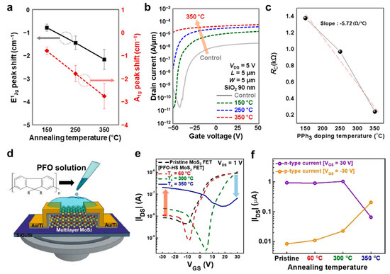
Figure 5.
(a) Raman peak shift values against the formation temperatures of PPh3 (black line: E2g1 peak, red line: A1g peak); (b) Transfer curve of pristine MoS2 FET and PPh3-doped MoS2 FET annealing at 3 different temperatures (150, 250, and 350 °C); (c) Contact resistance of PPh3-doped MoS2 FET measured at various annealing temperatures (black line: 150, 250, and 350 °C, red line: line profile of contact resistance); (adapted from [110] with permission from the American Chemical Society); (d) 3D schematic of PFO-doped MoS2 FET, where red spheres represent Mo atoms, and yellow spheres represent S atoms. The inset shows the chemical structure of poly(9,9-di-n-octylfluorenyl-2,7-diyl) (PFO); Electrical characteristics of the pristine MoS2 FET and PFO-doped MoS2 FET annealed at various temperature (60, 300, and 350 °C); (e) Transfer curve; (f) Extracted n- and p-type current variation (adapted from [111] with permission from the Elsevier B.V.).
In the demonstration, an ambipolar MoS2 FET with strong p-type conductivity was achieved through chemical doping and annealing effects. In 2021, Lee et al. spin-coated a 10 mg mL−1 solution of poly(9,9-di-n-octylfluorenyl-2,7-diyl) (PFO) onto the device and annealed it on a hotplate at various temperatures of 60, 300, and 350 °C for 10 min [111]. Figure 5d illustrates the 3D schematic diagram of the doping process of a PFO-doped MoS2 FET. Additionally, the electrical characteristics of a PFO-doped MoS2 FET were measured at various annealing temperatures (Figure 5e). The pristine MoS2 FET shows conventional n-type behavior and has 0.93 μA of on current at VG = 30 V and 102 A/A of on/off ratio. However, as the annealing temperature was increased, the PFO-doped MoS2 FET exhibited ambipolar behavior due to the enhanced p-type conductivity. Also, at an annealing temperature of 350 °C, the reduced n-type current and increased p-type current suggest ambipolar behavior of MoS2 FETs by PFO doping. Figure 5f shows the variation of n-type and p-type currents with pristine MoS2 FET and PFO-doped MoS2 FET. As PFO doping was performed and the annealing temperature increases, the p-type current gradually increases. Also, the p-type current of 350 °C annealed PFO-doped MoS2 FET was 0.20 μA with 24 times increase compared to the pristine MoS2 FET. On the other hand, the on current decreased 14 times from 0.93 μA to 0.06 μA.
5.2. Annealing and Chemical Doping Effects in MoTe2—Based Transistors
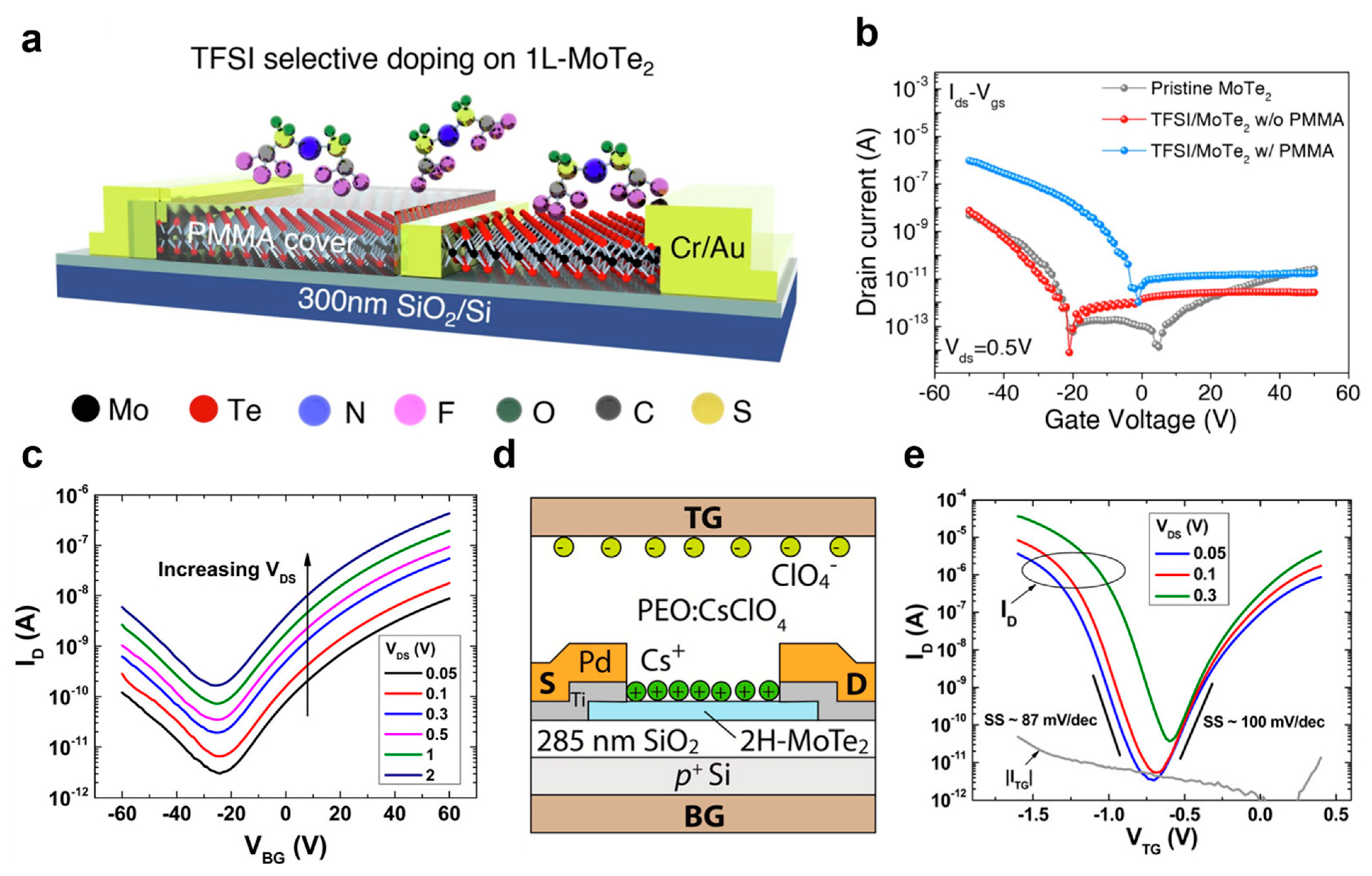
MoTe2 exhibits instability in the surrounding environment due to oxidation. The oxidation achieved p-type doping of the device and improved stability in the surrounding environment through bis(trifluoromethane)sulfonamide (TFSI) doping and PMMA encapsulation [112]. The mechanically exfoliated MoTe2 flakes were transferred onto a substrate and coated with PMMA, followed by annealing at 100 °C. The flakes and half of the electrodes were etched to expose the PMMA-coated device and the uncoated device. Subsequently, both samples were immersed in a nonreactive atmosphere for a 5 min period in a chlorobenzene (CB) solvent solution containing TFSI. Figure 6a illustrates a schematic diagram of the device. Chlorobenzene (CB), a chlorine—Based solvent containing lone electron pairs, can act as an electron donor to MoTe2, resulting in an n-type doping effect. However, the electron-donating effect is nullified by the electron-withdrawing effect of TFSI. Figure 6b illustrates the transfer characteristics of TSFI-MoTe2 FETs with and without a PMMA layer, compared to the pristine MoTe2 FET. After TSFI doping, the device without a PMMA layer exhibited unipolar p-type behavior with an on/off ratio exceeding 103 A/A and a maximum mobility of 0.58 cm2 V−1 s−1. The decrease in current in the n-branch indicates that TSFI induces p-type doping. The significant shift of the threshold voltage to 0 V after PMMA coating reflects the improved efficiency of TSFI doping for achieving p-type operation in the device. Conclusively, the device doped with TSFI along with a PMMA layer exhibited unipolar p-type behavior with an on/off ratio exceeding 106 A/A and a maximum mobility of 30 cm2 V−1 s−1, demonstrating a 250-fold improvement compared to the pristine device. This demonstrates superior on/off ratio and mobility enhancement characteristics compared to other doped TMD FETs.
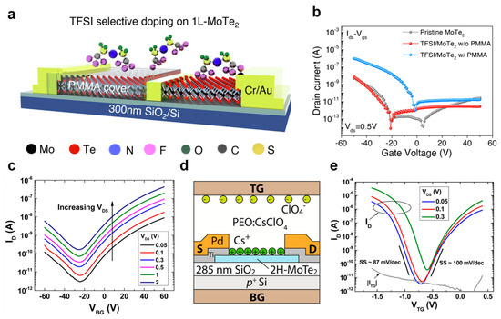
Figure 6.
(a) Structure of TFSI-MoTe2 with areas encapsulated by PMMA and those without encapsulation; (b) Transfer characteristics of pristine MoTe2 device compared to TFSI-MoTe2 with areas encapsulated by PMMA and those without encapsulation (adapted from [112] with permission from the Applied Surface Science); (c) Transfer curve of pristine MoTe2 FET with back-gate structure; (d) Cross section of ion gate MoTe2 FET; (e) Transfer curve of ion gate MoTe2 FET with various supply voltage (adapted from [113] with permission from the American Chemical Society).
The ambipolar MoTe2 FET doped with poly(ethylene oxide) (PEO) and CsClO4 as the top-gate dielectric exhibited both n-doping and p-doping effects [113]. The PEO:CsClO4 solution was drop cast on the pristine MoTe2 FET with back-gated structure and was annealed at 90 °C for 3 min. Figure 6c shows the transfer curve of a pristine MoTe2 FET. The pristine MoTe2 FET shows ambipolar behavior at various drain-source voltages (0.05 V to 2 V). Figure 6d shows a cross-section of a MoTe2 FET doped with a top-gate dielectric of PEO:CsClO4. To construct the ion gate, the PEO:CsClO4 with gate dielectric and palladium (Pd) top gate electrodes were sequentially deposited on the MoTe2 channel. A positive or negative gate voltage applied to the top gate electrode induces n-type and p-type doping, respectively. The positive gate voltage applied to the top gate electrode induces electrons in the channel due to Cs+ ions, resulting in n-type doping effect. On the other hand, a negative gate voltage results in p-type doping of MoTe2 due to ClO4− ions. Figure 6e shows the transfer curve of an ion-gate MoTe2 FET. Compared to pristine MoTe2 FETs, the on/off ratio and on current of ion-gate MoTe2 FET increased 20 times and 40 times in the n-branch and p-branch, respectively (VDS = 0.05 V).
5.3. Annealing and Chemical Doping Effects in WSe2—Based Transistors
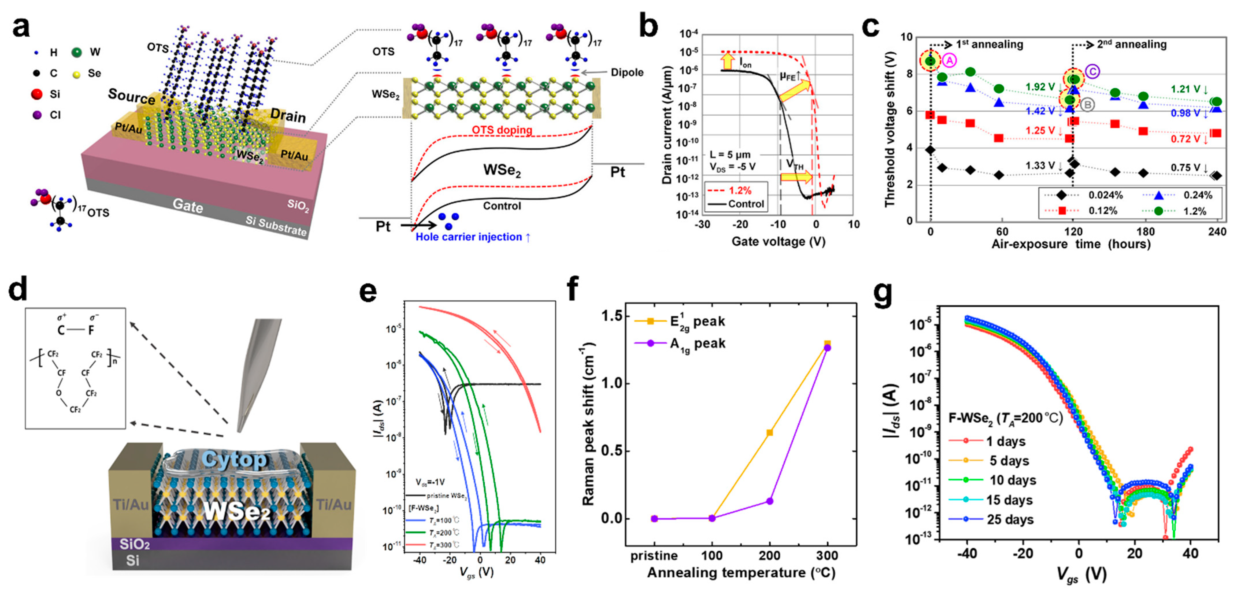
Using self-assembled monolayers (SAM) and a double annealing process, the changes in the characteristics of WSe2 FET was observed. The device was immersed in an octadecyl-trichlorosilane (OTS) solution, which served as the material for SAM, and annealed at 120 °C for 20 min [114]. Figure 7a shows the 3D schematic and energy band diagram of the OTS-doped WSe2 FET. The methyl groups of OTS doping on the WSe2 surface possess positive poles, and the electrons accumulate on the WSe2 surface due to the dipolar effect of OTS, resulting in the occurrence of a p-type doping effect. Also, as the concentration of OTS solution was increased, the p-type doping effect on WSe2 FET was enhanced. The OTS doping effect on WSe2 FETs reduces the Schottky barrier height. The upward valence band of the OTS-doped WSe2 FET enhances the hole injection by the narrowed tunneling barrier. Figure 7b shows the transfer curves of a pristine WSe2 FET and a WSe2 FET doped with OTS at a concentration of 1.2%. The pristine WSe2 FET has a threshold voltage of −9.1 V and on current of 1.64 × 10⁻⁶ A/μm. On the other hand, threshold voltage and on current of WSe2 FET doped with 1.2% OTS were −0.45 V and 1.42 × 10⁻⁵ A/μm, respectively. In addition, the mobility increased from 30 ± 4 cm2 V−1 s−1 (before doping) to 192 cm2 V−1 s−1 for the device doped with 0.024% OTS (~105 cm2 V−1 s−1 in the 1.2% OTS-doped device). Figure 7c shows the extracted threshold voltage of OTS-doped WSe2 FETs according to time in an air ambient. The threshold voltage of WSe2 FETs doped with various OTS concentrations (0.024, 0.24, 0.12, 1.2%) is shifted towards a negative gate voltage due to moisture in the air. However, an additional annealing process at 120 °C confirmed that shifts in the threshold voltage back to positive values restores the p-doping effect. The additional annealing process reduces the Si–O–Si bonds of OTS formed in an air exposure and increases the Si–OH bonds that enhance the p-doping effect.
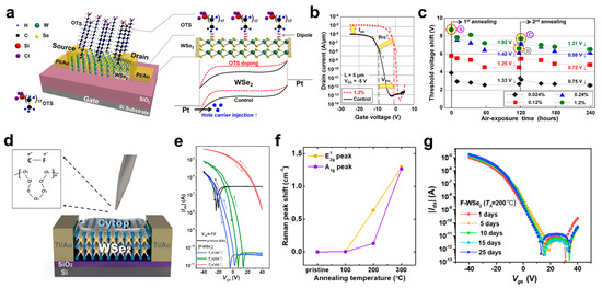
Figure 7.
(a) 3D structure and energy band diagram of OTS-doped WSe2 FET; (b) Transfer curve of pristine WSe2 FET and OTS-doped WSe2 FET; (c) Extracted threshold voltage of OTS-doped WSe2 FET according to air exposure time (adapted from [114] with permission from the American Chemical Society); (d) 3D schematic of CYTOP-doped WSe2 FET and inset shows the chemical structure of CYTOP; (e) Transfer curve of pristine WSe2 FET and CYTOP-doped WSe2 FET with various annealing temperature (100, 200, and 300 °C); (f) Raman peak shift of pristine WSe2 FET and CYTOP-doped WSe2 FET; (g) Electrical stability of CYTOP-doped WSe2 FET over 25 days in air condition (adapted from [115] with permission from the MDPI).
Meanwhile, In 2021, the p-doping effect of WSe2 FET was reported by means of the fluoropolymer CYTOP as a p-type dopant [115]. The pristine WSe2 FETs were coated with CYTOP solution and annealed at various temperatures (100, 200, and 300 °C). Figure 7d shows a 3D schematic of the CYTOP-doped WSe2 FET. The C–F bond of CYTOP coated on the WSe2 surface enhances hole accumulation, resulting in the increased p-type current. Figure 7e shows the transfer curves of pristine WSe2 FET and CYTOP-doped WSe2 FETs. The on and off currents of the pristine WSe2 FET are 2.30 × 10⁻⁶ A and 1.26 × 10⁻⁸ A, respectively. However, as CYTOP is doped and the annealing temperature increases, the p-type current increases and the n-type current significantly decreases. The off current of the CYTOP-doped WSe2 FET annealed at 100 °C is reduced to 8.46 × 10⁻¹² A. Subsequently, at the annealing temperature of 200 °C, the on current increases to 8.52 × 10⁻⁶ A. In particular, the CYTOP-doped WSe2 FET with 300 °C annealing processed has an on current of 4.10 × 10⁻⁵ A, which is 6 times higher than the initial value, and off current of 3.15 × 10⁻⁶ A. In addition, CYTOP coating and additional annealing treatments remove impurities on the surface of WSe2 and reduce hysteresis due to reduced traps. Also, the p-doping effect of CYTOP was investigated by Raman analysis (Figure 7f). The A1g and E2g1 peaks of CYTOP-coated WSe2 become blue shifted, and their values increase as the annealing temperature increases. At last, the electrical characteristics of a CYTOP-doped WSe2 FET annealed at 100 °C were stable for 25 days in air exposure (Figure 7g).
5.4. Annealing and Chemical Doping Effects in MoSe2 and WS2—Based Transistor
The molecular arrangement of poly-(diketopyrrolopyrrole terthiophene) (PDPP3T) can be controlled through the adjustment of annealing temperature. Yoo et al. demonstrated the n-doping effect in multilayer molybdenum diselenide (MoSe2) FET by doping PDPP3T [116]. In particular, at annealing temperatures above 200 °C, the molecular structure of PDPP3T changed edge-on state with molecules oriented vertically. As a result, the edge-on PDPP3T induced an enhanced charge transport effect to MoSe2 FET due to the superimposed molecular dipole moment. Figure 8a shows the 3D schematic of the PDPP3T-doped MoSe2 FET. The coated PDPP3T was annealed at various temperatures (100, 200, and 300 °C). Figure 8b shows the transfer curves of pristine MoSe2 FET and PDPP3T-doped MoSe2 FET according to the annealing temperature. The pristine MoSe2 FET had ambipolar behavior with enhanced p-type conductivity with 104 A/A of on/off ratio. Annealing temperatures of 100 °C and 200 °C slightly increase the n-type current and p-type current of the PDPP3T-doped MoSe2 FET. However, the annealing process at 300 °C increased the n-type current rapidly and decreased the p-type current. In particular, the n-type current of 1.5 × 10⁻⁶ A has improved 2000 times compared to the initial value of 7 × 10⁻¹⁰ A. Also, the PDPP3T-doped MoSe2 FET has enhanced photoresponsivity compared to the pristine device at different wavelengths of light (832, 638, and 405 nm) (Figure 8c). Also, a maximum photoresponsivity of 91.2 AW−1 was obtained when light with a wavelength of 638 nm is applied at an intensity of 20 mW/cm2.
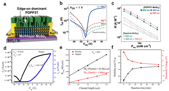
Figure 8.
(a) 3D schematic of PDPP3T-doped MoSe2 FET; (b) Transfer curve of pristine MoSe2 FET and PDPP3T-doped MoSe2 FET with various annealing temperatures (100, 200, and 300 °C); (c) comparison photoresponsivity under various light irradiation (832, 638, and 405 nm) (adapted from [116] with permission from the John Wiley and Sons); (d) Transfer curve of LiF-doped WS2 FET with log and linear scale; (e) Channel and contact resistance of pristine WS2 FET and LiF-doped WS2 FET according to channel length; (f) Extracted mobility and threshold voltage of LiF-doped WS2 FET with Lif immersing time (adapted from [117] with permission from the American Chemical Society).
The n-doping effect in WS2 FETs has been reported using lithium fluoride (LiF) as a dopant [117]. The pristine WS2 FET is immersed in 0.01 M of dopant solution and then annealed at 80 °C for 2 min to achieve the n-doping effect. Figure 8d shows the transfer curve of the n-type doped WS2 FET using LiF dopant. The on/off ratio and the threshold voltage of the pristine WS2 FET are 4.83 × 10⁵ A/A and 14 V, respectively. However, the LiF-doped WS2 FET has an on/off ratio of 1.05 × 10⁶ A/A and a threshold voltage of −6 V due to the negative shifted gate voltage. Also, the contact resistance was extracted using the transfer length method (TLM). Figure 8e shows the TLM resistance of the WS2 FET before and after doping according to the channel length. The doping effect of the WS2 FET on the LiF significantly reduces the channel and contact resistance, especially leading to the lowest contact resistance of 0.9 kΩ·μm. Figure 8f shows the changed mobility and threshold voltage according to LiF immersing time. As the immersion time in the LiF solution increases, the mobility increases, and the threshold voltage shifts towards the negative gate voltage. Also, the LiF immersing time of 120 min improves the mobility of the WS2 FET from 13.2 to 34.7 cm2 V−1 s−1.
Chemically doped TMDC FETs exhibit changes in electrical properties as both the TMDC and the chemical dopant are affected by the annealing process. Hence, to achieve the target electrical properties, optimized annealing conditions and appropriate chemical doping should be employed. Table 2 summarizes the post-annealing characteristics of chemically doped TMDC—Based transistors.

Table 2.
The annealing effect on the characteristics of TMDC—Based transistors doped with chemical dopants.
6. Conclusions and Future Aspect
This review discusses diverse techniques aimed at enhancing the electrical characteristics of transistors using TMDCs. The methods explored include annealing processes and chemical doping, which serve as effective means for engineering the electrical properties of TMDC transistors. Studies have examined the impact of annealing processes performed in various atmospheres, such as air, vacuum, and nitrogen, on the performance of TMDC—Based transistors. Additionally, the bandgap structure and Schottky barrier of TMDC can be controlled through functionalization with chemical dopants, such as polymers, SAMs, organic molecules, and inorganic compounds. Optimized annealing processes can further enhance the doping effect of TMDC—Based transistors.
However, several technological barriers remain to be addressed for the development and industrialization of annealing processing and chemical doping techniques for TMDC. Precise control of temperature, humidity, and ambient conditions during the TMDC annealing process is essential to achieve consistent experimental results. Ensuring uniform functionalization of dopants on the TMDC surface is crucial for accurately identifying the doping mechanism. Moreover, the thermal and chemical stability of the dopants should be considered to improve compatibility with subsequent processes. Efforts are ongoing to overcome these barriers through various technological advancements and research initiatives. Continuous optimization of research has significantly expanded the applicability of TMDC—Based devices in diverse fields, including photodetectors, neuromorphic sensors, and logic circuits. Innovative approaches, such as advanced annealing processes, chemical doping methods, integration with other materials, and the development of new device architectures, are actively being explored. As a result of these efforts, TMDC—Based FETs demonstrate great potential as semiconductor devices and are poised for success in industrialization. With the ongoing improvements and innovations, TMDC—Based FETs are expected to play a crucial role in various technological applications.
Author Contributions
Conceptualization: H.Y.; Literature survey: R.K. and D.H.L.; Writing draft: R.K. and D.H.L.; review and editing, R.K., D.H.L. and H.Y. All authors have read and agreed to the published version of the manuscript.
Funding
This work was supported by the Technology Innovation Program (00144300, Interface Technology of 3D Stacked Heterogeous System for SCM—Based Process-in-Memory) funded by the Ministry of Trade, Industry & Energy (MOTIE, Korea). This work was supported in part by the Gachon University Research Fund of 2021 (GCU-202106380001).
Institutional Review Board Statement
Not applicable.
Informed Consent Statement
Not applicable.
Data Availability Statement
Not applicable.
Conflicts of Interest
The authors declare no conflict of interest.
References
- Stankovich, S.; Dikin, D.A.; Dommett, G.H.; Kohlhaas, K.M.; Zimney, E.J.; Stach, E.A.; Piner, R.D.; Nguyen, S.T.; Ruoff, R.S. Graphene—Based composite materials. Nature 2006, 442, 282–286. [Google Scholar] [CrossRef] [PubMed]
- Tiwari, S.K.; Mishra, R.K.; Ha, S.K.; Huczko, A. Evolution of graphene oxide and graphene: From imagination to industrialization. ChemNanoMat 2018, 4, 598–620. [Google Scholar] [CrossRef]
- Hughes, Z.E.; Walsh, T.R. Computational chemistry for graphene—Based energy applications: Progress and challenges. Nanoscale 2015, 7, 6883–6908. [Google Scholar] [CrossRef] [PubMed]
- Tiwari, S.K.; Sahoo, S.; Wang, N.; Huczko, A. Graphene research and their outputs: Status and prospect. J. Sci. Adv. Mater. Dev. 2020, 5, 10–29. [Google Scholar]
- Chen, Y.; Wang, X.; Wang, P.; Huang, H.; Wu, G.; Tian, B.; Hong, Z.; Wang, Y.; Sun, S.; Shen, H. Optoelectronic properties of few-layer MoS2 FET gated by ferroelectric relaxor polymer. ACS Appl. Mater. Interfaces 2016, 8, 32083–32088. [Google Scholar] [CrossRef]
- Ghatak, S.; Pal, A.N.; Ghosh, A. Nature of electronic states in atomically thin MoS2 field-effect transistors. ACS Nano 2011, 5, 7707–7712. [Google Scholar] [CrossRef] [PubMed]
- Wang, Q.H.; Kalantar-Zadeh, K.; Kis, A.; Coleman, J.N.; Strano, M.S. Electronics and optoelectronics of two-dimensional transition metal dichalcogenides. Nat. Nanotechnol. 2012, 7, 699–712. [Google Scholar] [CrossRef]
- Cao, L. Two-dimensional transition-metal dichalcogenide materials: Toward an age of atomic-scale photonics. MRS Bull. 2015, 40, 592–599. [Google Scholar] [CrossRef]
- Movva, H.C.; Rai, A.; Kang, S.; Kim, K.; Fallahazad, B.; Taniguchi, T.; Watanabe, K.; Tutuc, E.; Banerjee, S.K. High-mobility holes in dual-gated WSe2 field-effect transistors. ACS Nano 2015, 9, 10402–10410. [Google Scholar] [CrossRef]
- Tang, H.; Shi, B.; Pan, Y.; Li, J.; Zhang, X.; Yan, J.; Liu, S.; Yang, J.; Xu, L.; Yang, J. Schottky contact in monolayer WS2 field-effect transistors. Adv. Theory Simul. 2019, 2, 1900001. [Google Scholar] [CrossRef]
- Iqbal, M.W.; Iqbal, M.Z.; Khan, M.F.; Shehzad, M.A.; Seo, Y.; Park, J.H.; Hwang, C.; Eom, J. High-mobility and air-stable single-layer WS2 field-effect transistors sandwiched between chemical vapor deposition-grown hexagonal BN films. Sci. Rep. 2015, 5, 10699. [Google Scholar] [CrossRef]
- Sajjad, M.; Singh, N.; Schwingenschlögl, U. Strongly bound excitons in monolayer PtS2 and PtSe2. Appl. Phys. Lett. 2018, 112, 043101. [Google Scholar] [CrossRef]
- Lu, J.; Zhang, X.; Su, G.; Yang, W.; Han, K.; Yu, X.; Wan, Y.; Wang, X.; Yang, P. Large-area uniform few-layer PtS2: Synthesis, structure and physical properties. Mater. Today Phys. 2021, 18, 100376. [Google Scholar] [CrossRef]
- Sato, Y.; Nishimura, T.; Duanfei, D.; Ueno, K.; Shinokita, K.; Matsuda, K.; Nagashio, K. Intrinsic electronic transport properties and carrier densities in PtS2 and SnSe2: Exploration of n+-Source for 2D tunnel FETs. Adv. Electron. Mater. 2021, 7, 2100292. [Google Scholar] [CrossRef]
- Yin, S.; Luo, Q.; Wei, D.; Guo, G.; Sun, X.; Tang, Y.; Dai, X. A type-II PtS2/MoTe2 van der Waals heterostructure with adjustable electronic and optical properties. Results Phys. 2022, 33, 105172. [Google Scholar] [CrossRef]
- Zhang, Y.; Feng, Q.; Hao, R.; Zhang, M. Fabrication of Large-Area Short-Wave Infrared Array Photodetectors under High Operating Temperature by High Quality PtS2 Continuous Films. Electronics 2022, 11, 838. [Google Scholar] [CrossRef]
- Bertolazzi, S.; Brivio, J.; Kis, A. Stretching and breaking of ultrathin MoS2. ACS Nano 2011, 5, 9703–9709. [Google Scholar] [CrossRef]
- Park, J.; Woo, H.; Jeon, S. Impact of fast transient charging and ambient on mobility of WS2 field-effect transistor. J. Vac. Sci. Technol. B 2017, 35, 050601. [Google Scholar] [CrossRef]
- Zeng, H.; Liu, G.-B.; Dai, J.; Yan, Y.; Zhu, B.; He, R.; Xie, L.; Xu, S.; Chen, X.; Yao, W.. Optical signature of symmetry variations and spin-valley coupling in atomically thin tungsten dichalcogenides. Sci. Rep. 2013, 3, 1608. [Google Scholar] [CrossRef]
- Wang, Z.; Li, Q.; Besenbacher, F.; Dong, M. Facile synthesis of single crystal PtSe2 nanosheets for nanoscale electronics. Adv. Mater. 2016, 28, 10224–10229. [Google Scholar] [CrossRef]
- AlMutairi, A.; Yin, D.; Yoon, Y. PtSe2 field-effect transistors: New opportunities for electronic devices. IEEE Electron Device Lett. 2017, 39, 151–154. [Google Scholar] [CrossRef]
- Pudasaini, P.R.; Oyedele, A.; Zhang, C.; Stanford, M.G.; Cross, N.; Wong, A.T.; Hoffman, A.N.; Xiao, K.; Duscher, G.; Mandrus, D.G. High-performance multilayer WSe2 field-effect transistors with carrier type control. Nano Res. 2018, 11, 722–730. [Google Scholar] [CrossRef]
- Lu, X.; Utama, M.I.B.; Lin, J.; Gong, X.; Zhang, J.; Zhao, Y.; Pantelides, S.T.; Wang, J.; Dong, Z.; Liu, Z. Large-area synthesis of monolayer and few-layer MoSe2 films on SiO2 substrates. Nano Lett. 2014, 14, 2419–2425. [Google Scholar] [CrossRef] [PubMed]
- Liu, X.; Yang, Y.; Hu, T.; Zhao, G.; Chen, C.; Ren, W. Vertical ferroelectric switching by in-plane sliding of two-dimensional bilayer WTe2. Nanoscale 2019, 11, 18575–18581. [Google Scholar] [CrossRef] [PubMed]
- Zhang, E.; Chen, R.; Huang, C.; Yu, J.; Zhang, K.; Wang, W.; Liu, S.; Ling, J.; Wan, X.; Lu, H.-Z. Tunable positive to negative magnetoresistance in atomically thin WTe2. Nano Lett. 2017, 17, 878–885. [Google Scholar] [CrossRef]
- Qu, D.; Liu, X.; Huang, M.; Lee, C.; Ahmed, F.; Kim, H.; Ruoff, R.S.; Hone, J.; Yoo, W.J. Carrier-type modulation and mobility improvement of thin MoTe2. Adv. Mater. 2017, 29, 1606433. [Google Scholar] [CrossRef]
- Choi, W.; Yin, D.; Choo, S.; Jeong, S.-H.; Kwon, H.-J.; Yoon, Y.; Kim, S. Low-temperature behaviors of multilayer MoS2 transistors with ohmic and Schottky contacts. Appl. Phys. Lett. 2019, 115, 033501. [Google Scholar] [CrossRef]
- Zou, T.; Kim, H.J.; Kim, S.; Liu, A.; Choi, M.Y.; Jung, H.; Zhu, H.; You, I.; Reo, Y.; Lee, W.J. High-Performance Solution-Processed 2D P-Type WSe2 Transistors and Circuits through Molecular Doping. Adv. Mater. 2023, 35, 2208934. [Google Scholar] [CrossRef] [PubMed]
- Fathipour, S.; Ma, N.; Hwang, W.; Protasenko, V.; Vishwanath, S.; Xing, H.; Xu, H.; Jena, D.; Appenzeller, J.; Seabaugh, A. Exfoliated multilayer MoTe2 field-effect transistors. Appl. Phys. Lett. 2014, 105, 192101. [Google Scholar] [CrossRef]
- Park, G.H.; Nielsch, K.; Thomas, A. 2D transition metal dichalcogenide thin films obtained by chemical gas phase deposition techniques. Adv. Mater. Interfaces 2019, 6, 1800688. [Google Scholar] [CrossRef]
- Patel, A.B.; Chauhan, P.; Machhi, H.K.; Narayan, S.; Sumesh, C.; Patel, K.; Soni, S.S.; Jha, P.; Solanki, G.; Pathak, V. Transferrable thin film of ultrasonically exfoliated MoSe2 nanocrystals for efficient visible-light photodetector. Phys. E Low Dimens. Syst. Nanostruct. 2020, 119, 114019. [Google Scholar] [CrossRef]
- Seo, S.G.; Ryu, J.H.; Lee, W.Y.; Jin, S.H. Visible Light Illumination Effects on Instability of MoS2 Thin-Film Transistors for Optical Sensor Application. Phys. Status Solidi A 2022, 219, 2200052. [Google Scholar] [CrossRef]
- Yang, Y.; Li, J.; Choi, S.; Jeon, S.; Cho, J.H.; Lee, B.H.; Lee, S. High-responsivity PtSe2 photodetector enhanced by photogating effect. Appl. Phys. Lett. 2021, 118, 013103. [Google Scholar] [CrossRef]
- Pham, T.; Li, G.; Bekyarova, E.; Itkis, M.E.; Mulchandani, A. MoS2—Based optoelectronic gas sensor with sub-parts-per-billion limit of NO2 gas detection. ACS Nano 2019, 13, 3196–3205. [Google Scholar] [CrossRef]
- Zong, B.; Li, Q.; Chen, X.; Liu, C.; Li, L.; Ruan, J.; Mao, S. Highly enhanced gas sensing performance using a 1T/2H Heterophase MoS2 field-effect transistor at room temperature. ACS Appl. Mater. Interfaces 2020, 12, 50610–50618. [Google Scholar] [CrossRef]
- Zheng, W.; Liu, X.; Xie, J.; Lu, G.; Zhang, J. Emerging van der Waals junctions based on TMDs materials for advanced gas sensors. Coord. Chem. Rev. 2021, 447, 214151. [Google Scholar] [CrossRef]
- Li, D. Nanofabrication Technologies for Making Neuromorphic Devices Based on Two-Dimensional MoS2. Ph.D. Thesis, University of Michigan, Ann Arbor, MI, USA, 2020. [Google Scholar]
- Sangwan, V.K.; Jariwala, D.; Kim, I.S.; Chen, K.-S.; Marks, T.J.; Lauhon, L.J.; Hersam, M.C. Gate-tunable memristive phenomena mediated by grain boundaries in single-layer MoS2. Nat. Nanotechnol. 2015, 10, 403–406. [Google Scholar] [CrossRef]
- Chen, S.; Mahmoodi, M.R.; Shi, Y.; Mahata, C.; Yuan, B.; Liang, X.; Wen, C.; Hui, F.; Akinwande, D.; Strukov, D.B. Wafer-scale integration of two-dimensional materials in high-density memristive crossbar arrays for artificial neural networks. Nat. Electron. 2020, 3, 638–645. [Google Scholar] [CrossRef]
- Bian, H.; Goh, Y.Y.; Liu, Y.; Ling, H.; Xie, L.; Liu, X. Stimuli-Responsive Memristive Materials for Artificial Synapses and Neuromorphic Computing. Adv. Mater. 2021, 33, 2006469. [Google Scholar] [CrossRef]
- Lee, H.W.; Kang, D.-H.; Cho, J.H.; Lee, S.; Jun, D.-H.; Park, J.-H. Highly sensitive and reusable membraneless field-effect transistor (FET)-type tungsten diselenide (WSe2) biosensors. ACS Appl. Mater. Interfaces 2018, 10, 17639–17645. [Google Scholar] [CrossRef]
- Park, H.; Han, G.; Lee, S.W.; Lee, H.; Jeong, S.H.; Naqi, M.; AlMutairi, A.; Kim, Y.J.; Lee, J.; Kim, W.-J. Label-free and recalibrated multilayer MoS2 biosensor for point-of-care diagnostics. ACS Appl. Mater. Interfaces 2017, 9, 43490–43497. [Google Scholar] [CrossRef] [PubMed]
- Ryu, B.; Nam, H.; Oh, B.-R.; Song, Y.; Chen, P.; Park, Y.; Wan, W.; Kurabayashi, K.; Liang, X. Cyclewise operation of printed MoS2 transistor biosensors for rapid biomolecule quantification at femtomolar levels. ACS Sens. 2017, 2, 274–281. [Google Scholar] [CrossRef] [PubMed]
- Fathi-Hafshejani, P.; Azam, N.; Wang, L.; Kuroda, M.A.; Hamilton, M.C.; Hasim, S.; Mahjouri-Samani, M. Two-dimensional-material—Based field-effect transistor biosensor for detecting COVID-19 virus (SARS-CoV-2). ACS Nano 2021, 15, 11461–11469. [Google Scholar] [CrossRef]
- Jeong, Y.; Shin, D.; Park, J.H.; Park, J.; Yi, Y.; Im, S. Integrated advantages from perovskite photovoltaic cell and 2D MoTe2 transistor towards self-power energy harvesting and photosensing. Nano Energy 2019, 63, 103833. [Google Scholar] [CrossRef]
- Lee, M.H.; Wu, W. 2D Materials for Wearable Energy Harvesting. Adv. Mater. Technol. 2022, 7, 2101623. [Google Scholar] [CrossRef]
- Tahir, M.B.; Fatima, U. Recent trends and emerging challenges in two-dimensional materials for energy harvesting and storage applications. Energy Storage 2022, 4, e244. [Google Scholar] [CrossRef]
- Taube, A.; Judek, J.; Łapińska, A.; Zdrojek, M. Temperature-dependent thermal properties of supported MoS2 monolayers. ACS Appl. Mater. Interfaces 2015, 7, 5061–5065. [Google Scholar] [CrossRef]
- Ahmed, S.; Viboon, P.; Ding, X.; Bao, N.; Du, Y.; Herng, T.; Ding, J.; Yi, J. Annealing effect on the ferromagnetism of MoS2 nanoparticles. J. Alloys Compd. 2018, 746, 399–404. [Google Scholar] [CrossRef]
- Kim, H.J.; Kim, D.; Jung, S.; Bae, M.H.; Yun, Y.J.; Yi, S.N.; Yu, J.S.; Kim, J.H.; Ha, D.H. Changes in the Raman spectra of monolayer MoS2 upon thermal annealing. J. Raman Spectrosc. 2018, 49, 1938–1944. [Google Scholar] [CrossRef]
- Lin, J.; Pantelides, S.T.; Zhou, W. Vacancy-induced formation and growth of inversion domains in transition-metal dichalcogenide monolayer. ACS Nano 2015, 9, 5189–5197. [Google Scholar] [CrossRef]
- Kim, S.; Hong, S.; Yoo, H. Control of Charge Transport Properties in Molybdenum Diselenide Field-Effect Transistors for Enhanced Noise-Margin and Inverter Characteristics. IEEE Trans. Nanotechnol. 2022, 21, 266–270. [Google Scholar] [CrossRef]
- Khan, M.A.; Mehmood, M.Q.; Massoud, Y. High-Temperature Annealing Effects on Atomically Thin Tungsten Diselenide Field-Effect Transistor. Appl. Sci. 2022, 12, 8119. [Google Scholar] [CrossRef]
- Xu, S.; Wu, Z.; Lu, H.; Han, Y.; Long, G.; Chen, X.; Han, T.; Ye, W.; Wu, Y.; Lin, J. Universal low-temperature Ohmic contacts for quantum transport in transition metal dichalcogenides. 2D Mater. 2016, 3, 021007. [Google Scholar] [CrossRef]
- Choi, Y.; Park, H.; Lee, N.; Kim, B.; Lee, J.; Lee, G.; Jeon, H. Deposition of the tin sulfide thin films using ALD and a vacuum annealing process for tuning the phase transition. J. Alloys Compd. 2022, 896, 162806. [Google Scholar] [CrossRef]
- Liu, X.; Islam, A.; Guo, J.; Feng, P.X.-L. Controlling polarity of MoTe2 transistors for monolithic complementary logic via Schottky contact engineering. ACS Nano 2020, 14, 1457–1467. [Google Scholar] [CrossRef]
- Wang, X.; Feng, H.; Wu, Y.; Jiao, L. Controlled synthesis of highly crystalline MoS2 flakes by chemical vapor deposition. J. Am. Chem. Soc. 2013, 135, 5304–5307. [Google Scholar] [CrossRef]
- Tongay, S.; Zhou, J.; Ataca, C.; Liu, J.; Kang, J.S.; Matthews, T.S.; You, L.; Li, J.; Grossman, J.C.; Wu, J. Broad-range modulation of light emission in two-dimensional semiconductors by molecular physisorption gating. Nano Lett. 2013, 13, 2831–2836. [Google Scholar] [CrossRef]
- Ueno, K.; Fukushima, K. Changes in structure and chemical composition of α-MoTe2 and β-MoTe2 during heating in vacuum conditions. Appl. Phys. Express 2015, 8, 095201. [Google Scholar] [CrossRef]
- Kim, Y.J.; Park, W.; Yang, J.H.; Kim, Y.; Lee, B.H. Contact resistance reduction of WS2 FETs using high-pressure hydrogen annealing. IEEE J. Electron Devices Soc. 2017, 6, 164–168. [Google Scholar] [CrossRef]
- Park, H.; Son, J.; Kim, J. Reducing the contact and channel resistances of black phosphorus via low-temperature vacuum annealing. J. Mater. Chem. C 2018, 6, 1567–1572. [Google Scholar] [CrossRef]
- Chow, W.L.; Yu, P.; Liu, F.; Hong, J.; Wang, X.; Zeng, Q.; Hsu, C.H.; Zhu, C.; Zhou, J.; Wang, X. High mobility 2D palladium diselenide field-effect transistors with tunable ambipolar characteristics. Adv. Mater. 2017, 29, 1602969. [Google Scholar] [CrossRef]
- Yang, C.-M.; Chen, T.-C.; Yang, Y.-C.; Meyyappan, M. Annealing effect on UV-illuminated recovery in gas response of graphene—Based NO2 sensors. RSC Adv. 2019, 9, 23343–23351. [Google Scholar] [CrossRef] [PubMed]
- Chen, W.-H.; Kawakami, N.; Hsueh, J.-W.; Kuo, L.-H.; Chen, J.-Y.; Liao, T.-W.; Kuo, C.-N.; Lue, C.-S.; Lai, Y.-L.; Hsu, Y.-J. Toward Perfect Surfaces of Transition Metal Dichalcogenides with Ion Bombardment and Annealing Treatment. ACS Appl. Mater. Interfaces 2023, 15, 16153–16161. [Google Scholar] [CrossRef] [PubMed]
- Merve, A.; ERTUGRUL, M. Investigation of the dependence of ambipolarity on channel thickness for TMDC based field effect transistors. Erzincan Univ. J. Sci. Technol. 2021, 14, 825–836. [Google Scholar]
- Kim, I.S.; Sangwan, V.K.; Jariwala, D.; Wood, J.D.; Park, S.; Chen, K.-S.; Shi, F.; Ruiz-Zepeda, F.; Ponce, A.; Jose-Yacaman, M. Influence of stoichiometry on the optical and electrical properties of chemical vapor deposition derived MoS2. ACS Nano 2014, 8, 10551–10558. [Google Scholar] [CrossRef]
- Golovynskyi, S.; Irfan, I.; Bosi, M.; Seravalli, L.; Datsenko, O.I.; Golovynska, I.; Li, B.; Lin, D.; Qu, J. Exciton and trion in few-layer MoS2: Thickness-and temperature-dependent photoluminescence. Appl. Surf. Sci. 2020, 515, 146033. [Google Scholar] [CrossRef]
- Si, K.; Ma, J.; Guo, Y.; Zhou, Y.; Lu, C.; Xu, X.; Xu, X. Improving photoelectric performance of MoS2 photoelectrodes by annealing. Ceram. Int. 2018, 44, 21153–21158. [Google Scholar] [CrossRef]
- Choi, J.; Zhang, H.; Choi, J.H. Modulating optoelectronic properties of two-dimensional transition metal dichalcogenide semiconductors by photoinduced charge transfer. ACS Nano 2016, 10, 1671–1680. [Google Scholar] [CrossRef]
- Kufer, D.; Konstantatos, G. Highly sensitive, encapsulated MoS2 photodetector with gate controllable gain and speed. Nano Lett. 2015, 15, 7307–7313. [Google Scholar] [CrossRef]
- Chaves, A.; Azadani, J.G.; Alsalman, H.; Da Costa, D.; Frisenda, R.; Chaves, A.; Song, S.H.; Kim, Y.D.; He, D.; Zhou, J. Bandgap engineering of two-dimensional semiconductor materials. NPJ 2D Mater. Appl. 2020, 4, 29. [Google Scholar] [CrossRef]
- Iacovella, F.; Koroleva, A.; Rybkin, A.G.; Fouskaki, M.; Chaniotakis, N.; Savvidis, P.; Deligeorgis, G. Impact of thermal annealing in forming gas on the optical and electrical properties of MoS2 monolayer. J. Phys. Condens. Matter 2020, 33, 035001. [Google Scholar] [CrossRef] [PubMed]
- Frisenda, R.; Drüppel, M.; Schmidt, R.; Michaelis de Vasconcellos, S.; Perez de Lara, D.; Bratschitsch, R.; Rohlfing, M.; Castellanos-Gomez, A. Biaxial strain tuning of the optical properties of single-layer transition metal dichalcogenides. NPJ 2D Mater. Appl. 2017, 1, 10. [Google Scholar] [CrossRef]
- Chee, S.-S.; Oh, C.; Son, M.; Son, G.-C.; Jang, H.; Yoo, T.J.; Lee, S.; Lee, W.; Hwang, J.Y.; Choi, H. Sulfur vacancy-induced reversible doping of transition metal disulfides via hydrazine treatment. Nanoscale 2017, 9, 9333–9339. [Google Scholar] [CrossRef] [PubMed]
- Eda, G.; Yamaguchi, H.; Voiry, D.; Fujita, T.; Chen, M.; Chhowalla, M. Photoluminescence from chemically exfoliated MoS2. Nano Lett. 2011, 11, 5111–5116. [Google Scholar] [CrossRef] [PubMed]
- Allain, A.; Kis, A. Electron and hole mobilities in single-layer WSe2. ACS Nano 2014, 8, 7180–7185. [Google Scholar] [CrossRef] [PubMed]
- Baugher, B.W.; Churchill, H.O.; Yang, Y.; Jarillo-Herrero, P. Intrinsic electronic transport properties of high-quality monolayer and bilayer MoS2. Nano Lett. 2013, 13, 4212–4216. [Google Scholar] [CrossRef] [PubMed]
- Shahbazi, M.; Khanlary, M.R. Study of optical, electrochemical, and morphological properties of MoS2 thin films prepared by thermal evaporation. Braz. J. Phys. 2021, 51, 1182–1190. [Google Scholar] [CrossRef]
- Yang, R.; Zheng, X.; Wang, Z.; Miller, C.J.; Feng, P.X.-L. Multilayer MoS2 transistors enabled by a facile dry-transfer technique and thermal annealing. J. Vac. Sci. Technol. B 2014, 32, 061203. [Google Scholar] [CrossRef]
- Klots, A.; Newaz, A.; Wang, B.; Prasai, D.; Krzyzanowska, H.; Lin, J.; Caudel, D.; Ghimire, N.; Yan, J.; Ivanov, B. Probing excitonic states in suspended two-dimensional semiconductors by photocurrent spectroscopy. Sci. Rep. 2014, 4, 6608. [Google Scholar] [CrossRef]
- Islam, Z.; Kozhakhmetov, A.; Robinson, J.; Haque, A. Enhancement of WSe2 FET Performance Using Low-Temperature Annealing. J. Electron. Mater. 2020, 49, 3770–3779. [Google Scholar] [CrossRef]
- Zhang, S.; Li, R.; Yao, Z.; Liao, P.; Li, Y.; Tian, H.; Wang, J.; Liu, P.; Guo, J.; Liu, K. Laser annealing towards high-performance monolayer MoS2 and WSe2 field effect transistors. Nanotechnology 2020, 31, 30LT02. [Google Scholar] [CrossRef] [PubMed]
- Wang, X.; Gong, Y.; Shi, G.; Chow, W.L.; Keyshar, K.; Ye, G.; Vajtai, R.; Lou, J.; Liu, Z.; Ringe, E. Chemical vapor deposition growth of crystalline monolayer MoSe2. ACS Nano 2014, 8, 5125–5131. [Google Scholar] [CrossRef]
- Shi, Y.; Zhou, W.; Lu, A.-Y.; Fang, W.; Lee, Y.-H.; Hsu, A.L.; Kim, S.M.; Kim, K.K.; Yang, H.Y.; Li, L.-J. Van der Waals epitaxy of MoS2 layers using graphene as growth templates. Nano Lett. 2012, 12, 2784–2791. [Google Scholar] [CrossRef] [PubMed]
- Mirabelli, G.; Walsh, L.A.; Gity, F.; Bhattacharjee, S.; Cullen, C.P.; Coileáin, C.Ó.; Monaghan, S.; McEvoy, N.; Nagle, R.; Hurley, P.K. Effects of annealing temperature and ambient on metal/PtSe2 contact alloy formation. ACS Omega 2019, 4, 17487–17493. [Google Scholar] [CrossRef]
- Lee, D.; Jang, J.H.; Song, W.; Moon, J.; Kim, Y.; Lee, J.; Jeong, B.; Park, S. In situ work-function measurement during chemical transformation of MoS2 to MoO3 by ambient-pressure x-ray photoelectron spectroscopy. 2D Mater. 2020, 7, 025014. [Google Scholar] [CrossRef]
- Wu, J.; Li, H.; Yin, Z.; Li, H.; Liu, J.; Cao, X.; Zhang, Q.; Zhang, H. Layer thinning and etching of mechanically exfoliated MoS2 nanosheets by thermal annealing in air. Small 2013, 9, 3314–3319. [Google Scholar]
- Liu, X.; Choi, M.S.; Hwang, E.; Yoo, W.J.; Sun, J. Fermi level pinning dependent 2D semiconductor devices: Challenges and prospects. Adv. Mater. 2022, 34, 2108425. [Google Scholar] [CrossRef]
- Wang, Y.; Liu, S.; Li, Q.; Quhe, R.; Yang, C.; Guo, Y.; Zhang, X.; Pan, Y.; Li, J.; Zhang, H. Schottky barrier heights in two-dimensional field-effect transistors: From theory to experiment. Rep. Prog. Phys. 2021, 84, 056501. [Google Scholar] [CrossRef]
- Malavika, C.; Roshini, R.A.; Kanthi, R.S.; Kannan, E. Single crystal flake parameters of MoS2 and MoSe2 exfoliated using anodic bonding technique and its potential in rapid prototyping. J. Phys. Commun. 2020, 4, 105015. [Google Scholar] [CrossRef]
- Heyl, M.; List-Kratochvil, E.J. Only gold can pull this off: Mechanical exfoliations of transition metal dichalcogenides beyond scotch tape. Appl. Phys. A 2023, 129, 16. [Google Scholar] [CrossRef]
- Novoselov, K.S.; Geim, A.K.; Morozov, S.V.; Jiang, D.-E.; Zhang, Y.; Dubonos, S.V.; Grigorieva, I.V.; Firsov, A.A. Electric field effect in atomically thin carbon films. Science 2004, 306, 666–669. [Google Scholar] [CrossRef] [PubMed]
- Hoang, A.T.; Qu, K.; Chen, X.; Ahn, J.-H. Large-area synthesis of transition metal dichalcogenides via CVD and solution—Based approaches and their device applications. Nanoscale 2021, 13, 615–633. [Google Scholar] [CrossRef] [PubMed]
- Wang, J.; Li, T.; Wang, Q.; Wang, W.; Shi, R.; Wang, N.; Amini, A.; Cheng, C. Controlled growth of atomically thin transition metal dichalcogenides via chemical vapor deposition method. Mater. Today Adv. 2020, 8, 100098. [Google Scholar] [CrossRef]
- Bernal, M.; Álvarez, L.; Giovanelli, E.; Arnáiz, A.; Ruiz-González, L.; Casado, S.; Granados, D.; Pizarro, A.; Castellanos-Gomez, A.; Pérez, E. Luminescent Transition Metal Dichalcogenide Nanosheets through One-Step Liquid Phase Exfoliation. 2D Mater. 2016, 3, 035014. [Google Scholar] [CrossRef]
- Coleman, J.N.; Lotya, M.; O’Neill, A.; Bergin, S.D.; King, P.J.; Khan, U.; Young, K.; Gaucher, A.; De, S.; Smith, R.J. Two-dimensional nanosheets produced by liquid exfoliation of layered materials. Science 2011, 331, 568–571. [Google Scholar] [CrossRef]
- Yang, G.; Fang, X.; Gu, Y.; Danner, A.; Xie, F.; Zhang, X.; Lu, N.; Wang, Y.; Hua, B.; Gu, X. Insights on the enhanced Raman scattering of monolayer TMDCs (Mo, W)(S, Se)2 with Ag nanoparticles via rapid thermal annealing. Appl. Surf. Sci. 2020, 520, 146367. [Google Scholar] [CrossRef]
- Hu, W.; Wang, Y.; He, K.; He, X.; Bai, Y.; Liu, C.; Zhou, N.; Wang, H.; Li, P.; Ma, X. Straining of atomically thin WSe2 crystals: Suppressing slippage by thermal annealing. J. Appl. Phys. 2022, 132, 085104. [Google Scholar] [CrossRef]
- Jin, Z.; Shin, S.; Han, S.-J.; Min, Y.-S. Novel chemical route for atomic layer deposition of MoS2 thin film on SiO2/Si substrate. Nanoscale 2014, 6, 14453–14458. [Google Scholar] [CrossRef]
- Etzkorn, J.; Therese, H.A.; Rocker, F.; Zink, N.; Kolb, U.; Tremel, W. Metal-Organic Chemical Vapor Depostion Synthesis of Hollow Inorganic-Fullerene-Type MoS2 and MoSe2 Nanoparticles. Adv. Mater. 2005, 17, 2372–2375. [Google Scholar] [CrossRef]
- Kosmala, T.; Palczynski, P.; Amati, M.; Gregoratti, L.; Sezen, H.; Mattevi, C.; Agnoli, S.; Granozzi, G. Strain Induced Phase Transition of WS2 by Local Dewetting of Au/Mica Film upon Annealing. Surfaces 2020, 4, 1–8. [Google Scholar] [CrossRef]
- Namgung, S.D.; Yang, S.; Park, K.; Cho, A.-J.; Kim, H.; Kwon, J.-Y. Influence of post-annealing on the off current of MoS2 field-effect transistors. Nanoscale Res. Lett. 2015, 10, 62. [Google Scholar] [CrossRef] [PubMed]
- Islam, A.; Lee, J.; Feng, P.X.-L. All-dry transferred single-and few-layer MoS2 field effect transistor with enhanced performance by thermal annealing. J. Appl. Phys. 2018, 123, 025701. [Google Scholar] [CrossRef]
- Choi, M.S.; Lee, M.; Ngo, T.D.; Hone, J.; Yoo, W.J. Chemical Dopant-Free Doping by Annealing and Electron Beam Irradiation on 2D Materials. Adv. Electron. Mater. 2021, 7, 2100449. [Google Scholar] [CrossRef]
- Liu, J.; Wang, Y.; Xiao, X.; Zhang, K.; Guo, N.; Jia, Y.; Zhou, S.; Wu, Y.; Li, Q.; Xiao, L. Conversion of multi-layered MoTe2 transistor between P-type and N-type and their use in inverter. Nanoscale Res. Lett. 2018, 13, 291. [Google Scholar] [CrossRef]
- Bandyopadhyay, A.S.; Saenz, G.A.; Kaul, A.B. Role of metal contacts and effect of annealing in high performance 2D WSe2 field-effect transistors. Surf. Coat. Technol. 2020, 381, 125084. [Google Scholar] [CrossRef]
- Seo, J.; Cho, K.; Lee, W.; Shin, J.; Kim, J.-K.; Kim, J.; Pak, J.; Lee, T. Effect of Facile p-Doping on Electrical and Optoelectronic Characteristics of Ambipolar WSe2 Field-Effect Transistors. Nanoscale Res. Lett. 2019, 14, 313. [Google Scholar] [CrossRef]
- Ji, M.; Choi, W. Performance enhancement of WS2 transistors via double annealing. Microelectron. Eng. 2022, 255, 111709. [Google Scholar] [CrossRef]
- Tang, B.; Yu, Z.G.; Huang, L.; Chai, J.; Wong, S.L.; Deng, J.; Yang, W.; Gong, H.; Wang, S.; Ang, K.-W. Direct n- to p-type channel conversion in monolayer/few-layer WS2 field-effect transistors by atomic nitrogen treatment. ACS Nano 2018, 12, 2506–2513. [Google Scholar] [CrossRef]
- Heo, K.; Jo, S.-H.; Shim, J.; Kang, D.-H.; Kim, J.-H.; Park, J.-H. Stable and reversible triphenylphosphine—Based n-type doping technique for molybdenum disulfide (MoS2). ACS Appl. Mater. Interfaces 2018, 10, 32765–32772. [Google Scholar] [CrossRef]
- Lee, D.H.; Yun, H.J.; Hong, S.; Yoo, H. Ambipolar conduction and multicolor photosensing behaviors from poly (9,9-di-n-octylfluorenyl-2,7-diyl)-molybdenum disulfide heterointerfaces. Surf. Interfaces 2021, 27, 101448. [Google Scholar] [CrossRef]
- Nguyen, P.H.; Nguyen, D.H.; Kim, H.; Jeong, H.M.; Oh, H.M.; Jeong, M.S. Synergistic hole-doping on ultrathin MoTe2 for highly stable unipolar field-effect transistor. Appl. Surf. Sci. 2022, 596, 153567. [Google Scholar] [CrossRef]
- Xu, H.; Fathipour, S.; Kinder, E.W.; Seabaugh, A.C.; Fullerton-Shirey, S.K. Reconfigurable ion gating of 2H-MoTe2 field-effect transistors using poly (ethylene oxide)-CsClO4 solid polymer electrolyte. ACS Nano 2015, 9, 4900–4910. [Google Scholar] [CrossRef] [PubMed]
- Kang, D.-H.; Shim, J.; Jang, S.K.; Jeon, J.; Jeon, M.H.; Yeom, G.Y.; Jung, W.-S.; Jang, Y.H.; Lee, S.; Park, J.-H. Controllable nondegenerate p-type doping of tungsten diselenide by octadecyltrichlorosilane. ACS Nano 2015, 9, 1099–1107. [Google Scholar] [CrossRef] [PubMed]
- Lee, H.; Hong, S.; Yoo, H. Interfacial doping effects in fluoropolymer-tungsten diselenide composites providing high-performance P-type transistors. Polymers 2021, 13, 1087. [Google Scholar] [CrossRef]
- Yoo, H.; Hong, S.; Moon, H.; On, S.; Ahn, H.; Lee, H.K.; Kim, S.; Hong, Y.K.; Kim, J.J. Chemical doping effects on CVD-grown multilayer MoSe2 transistor. Adv. Electron. Mater. 2018, 4, 1700639. [Google Scholar] [CrossRef]
- Khalil, H.M.; Khan, M.F.; Eom, J.; Noh, H. Highly stable and tunable chemical doping of multilayer WS2 field effect transistor: Reduction in contact resistance. ACS Appl. Mater. Interfaces 2015, 7, 23589–23596. [Google Scholar] [CrossRef] [PubMed]
Disclaimer/Publisher’s Note: The statements, opinions and data contained in all publications are solely those of the individual author(s) and contributor(s) and not of MDPI and/or the editor(s). MDPI and/or the editor(s) disclaim responsibility for any injury to people or property resulting from any ideas, methods, instructions or products referred to in the content. |
© 2023 by the authors. Licensee MDPI, Basel, Switzerland. This article is an open access article distributed under the terms and conditions of the Creative Commons Attribution (CC BY) license (https://creativecommons.org/licenses/by/4.0/).


