Article

Raman Spectroscopy of V4O7 Films

1
Research and Educational Center “Functional Nanomaterials”, Baltic Federal University, Aleksandra Nevskogo 14, 236041 Kaliningrad, Russia
2
Deutsches Elektronen-Synchrotron (DESY), Notkestr. 85, 22607 Hamburg, Germany
*
Author to whom correspondence should be addressed.
Coatings 2022, 12(3), 291; https://doi.org/10.3390/coatings12030291
Submission received: 23 December 2021 / Revised: 7 February 2022 / Accepted: 14 February 2022 / Published: 22 February 2022
(This article belongs to the Special Issue Structure and Phase Transformations in Thin Films)

Abstract

:
A thin film of vanadium oxide Magnéli phase V4O7 was produced using cathodic arc sputtering. X-ray diffraction, Rutherford backscattering spectrometry and Raman investigations confirmed the formation of this phase. The Raman spectrum of V4O7 differs considerably from the spectrum of another Magnéli oxide, V3O5, showing that Raman spectroscopy is an excellent tool for distinguishing between these two phases. Temperature-dependent Raman measurements revealed a significant change of the spectra near the V4O7 metal–insulator phase transition.

1. Introduction

V4O7 belongs to a series of vanadium oxides with a general formula of VnO2n−1 (n = 3–9) called Magnéli phases [1]. All these phases can be described as modifications of the rutile structure with periodic sheared planes resembling stacking faults into which extra planes of metal atoms are introduced [2]. All Magnéli phases, except V7O13, undergo a metal–insulator transition with a little discontinuity in lattice constants [3]. For V4O7, such transition is observed between 237 and 250 K [3,4]. At room temperature, V4O7 is metallic, it has a triclinic structure and may be described in space group A 1 ¯ (four vanadium and seven oxygen atoms per unit cell with parameters of a = 5.509 Å, b = 7.008 Å, c = 12.258 Å, α = 95.09°, β = 95.19°, γ = 109.21° at 298 K) [5]. Below 250 K, the resistivity increases discontinuously by a factor of 8–50, the lattice symmetry is unchanged, and there are only slight changes of lattice constants or atomic positions [4,5].
The similarity of structures of Magnéli phases may make it challenging to identify the phase precisely using X-ray diffraction, especially if the sample is nanostructured (for instance, thin film), highly textured and has large lattice stress. Recently, we showed that Raman spectroscopy could be very sensitive to tiny variations of the crystal structure by measuring the spectral features of V3O5 around the phase transition at ~420 K [6]. Later, our results were further developed and fully confirmed by the other group [7]. Meanwhile, Raman scattering features for V4O7 (as well as for the other Magnéli phases with higher n) remain an open question. The only recent report claiming the synthesis and Raman characterization of V4O7 demonstrate the typical spectrum of V2O5, probably due to sample degradation during the measurement or the presence of impurities, was compiled in [8].
From the practical point of view, V4O7 shows potential as a thin film material for smart windows, optical switching and liquid crystal displays [9]. V4O7 nanoflakes demonstrate good performance as a photocatalyst [8], V4O7 nanowires may be used as optical sensors [10], and V4O7 nanocrosses are considered a promising candidate as a cathode for lithium-ion batteries [11].
Typically, V4O7 is produced from a mixture of V2O3 and V2O5 powders by vacuum heating [1,3] or vapor transport using TeCl4 [4,5,12]. Alternatively, this Magnéli phase can be obtained by solvothermal methods [8,9,10,11]. Direct sputtering of vanadium in an oxygen atmosphere can also yield V4O7, but such reports are scarce [13]. In our work, we used cathodic arc sputtering of vanadium target in reactive oxygen, and under certain conditions, V4O7 films were formed. We studied these films using Raman spectroscopy at room and low temperatures and showed that the phase transition significantly influenced the observed spectra.

2. Materials and Methods

Vanadium oxide films were deposited by a cathodic arc sputtering of a vanadium target in an oxygen atmosphere, similarly to our previous work [6]. The substrate was 10 mm × 10 mm (111)-oriented Si crystal with ~200 nm thermally grown oxide layer SiO2. The substrate temperature during the deposition was 600 °C, and the pressure of reactive oxygen was 0.045 Pa. The arc current was 55 A. The sample was placed about 50 cm away from the cathode, at the point where growth speed was about 17 nm/min. The total deposition time was 15 min, yielding a thickness of about 250 nm.
An X-ray diffraction (XRD) study of the films in θ–2θ geometry was performed using a Bruker AXS D8 DISCOVER setup with a Cu Kα (0.15418 nm) radiation (Bruker, Karlsruhe, Germany). Temperature-dependent measurements were performed using the Anton Paar temperature control unit in the range of −120~+100 °C.
Raman scattering measurements were performed using a Horiba Jobin Yvon micro-Raman spectrometer LabRam HR800 with an ×100 magnification objective lens (numerical aperture of 0.9, Horiba, Villeneuve d’Ascq, France). Measurements were conducted at room and lower temperatures in the argon environment to avoid water condensation on the sample. Peltier element supplied by Kryotherm, Saint-Petersburg, Russia, was used to achieve temperatures of up to −75 °C. A He-Ne laser with a 632.8 nm wavelength was used to excite Raman scattering. Laser power on the sample was 0.5 mW, and a spot diameter was about 10 μm (it was intentionally defocused to avoid sample degradation and reduce overheating). The total acquisition time for each sample was at least 1 h.
Stoichiometry of produced samples was investigated by Rutherford backscattering spectrometry (RBS) using the Van de Graaff accelerator AN2500 (High Voltage Engineering Europa B.V., Amersfoort, The Netherlands) located at Immanuel Kant Baltic Federal University (Kaliningrad, Russia). A sample was exposed to a 1.5 MeV 4He+ beam. An angle between the beam and normal to the sample surface was 5°, an exit angle was 21°, and a scattering angle was 160°. A beam current and a total accumulated charge were about 20 nA and 65 μC, respectively. Experimental spectra were processed using SIMNRA software (version: 7.03) [14].
Morphology of the samples was investigated using the atomic force microscope (AFM) SmartSPM Aist-NT in the tapping mode (amplitude 25 nm, AIST-NT Inc., Novato, CA, USA) and the scanning electron microscope (SEM) Zeiss Cross Beam XB 540 (Carl Zeiss Microscopy GmbH, Oberkochen, Germany), which is part of a unique scientific facility «SynchrotronLike», operated at 3 kV.

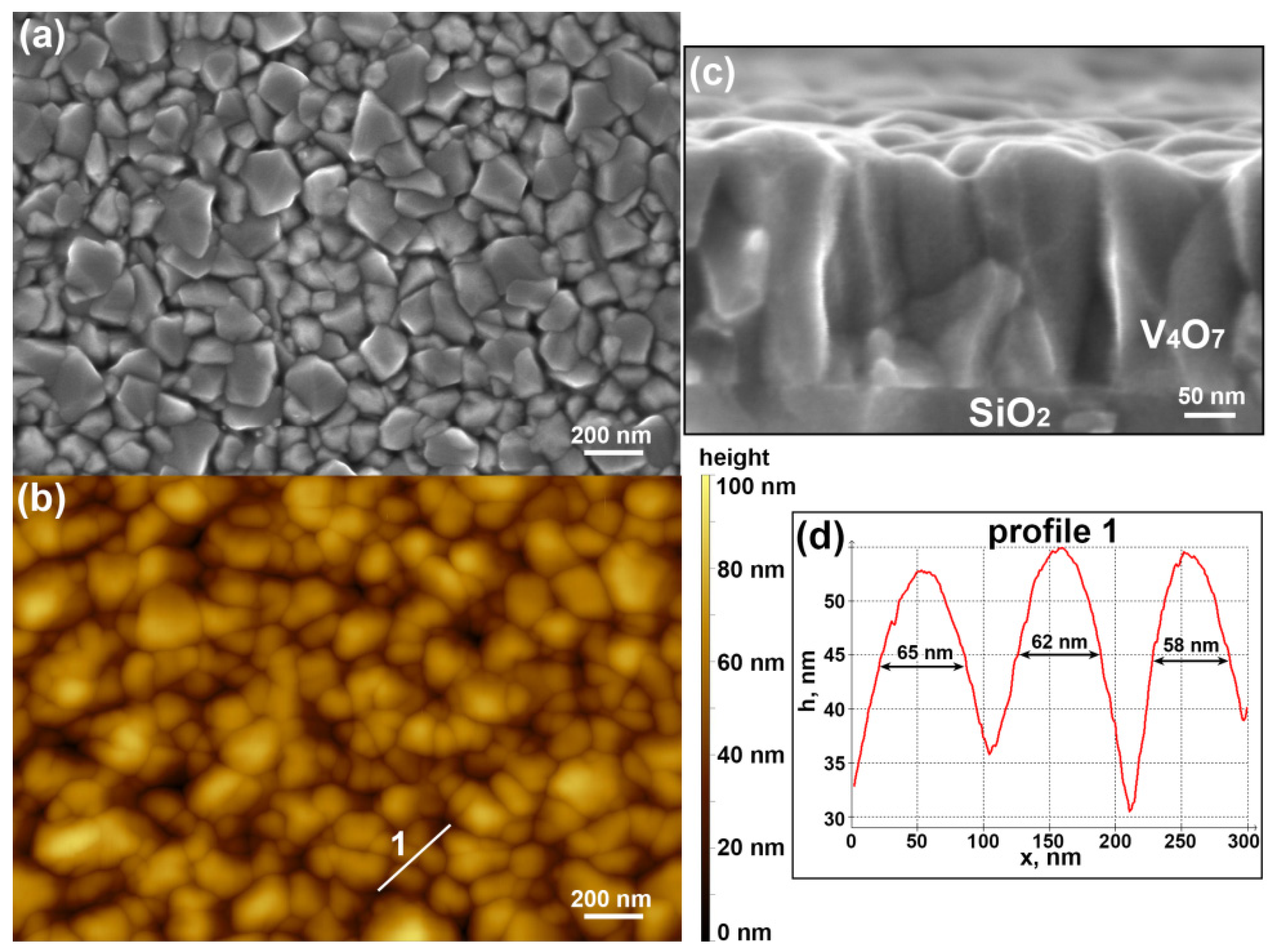
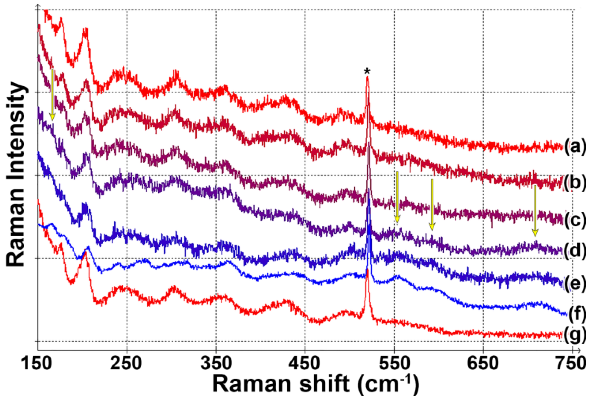
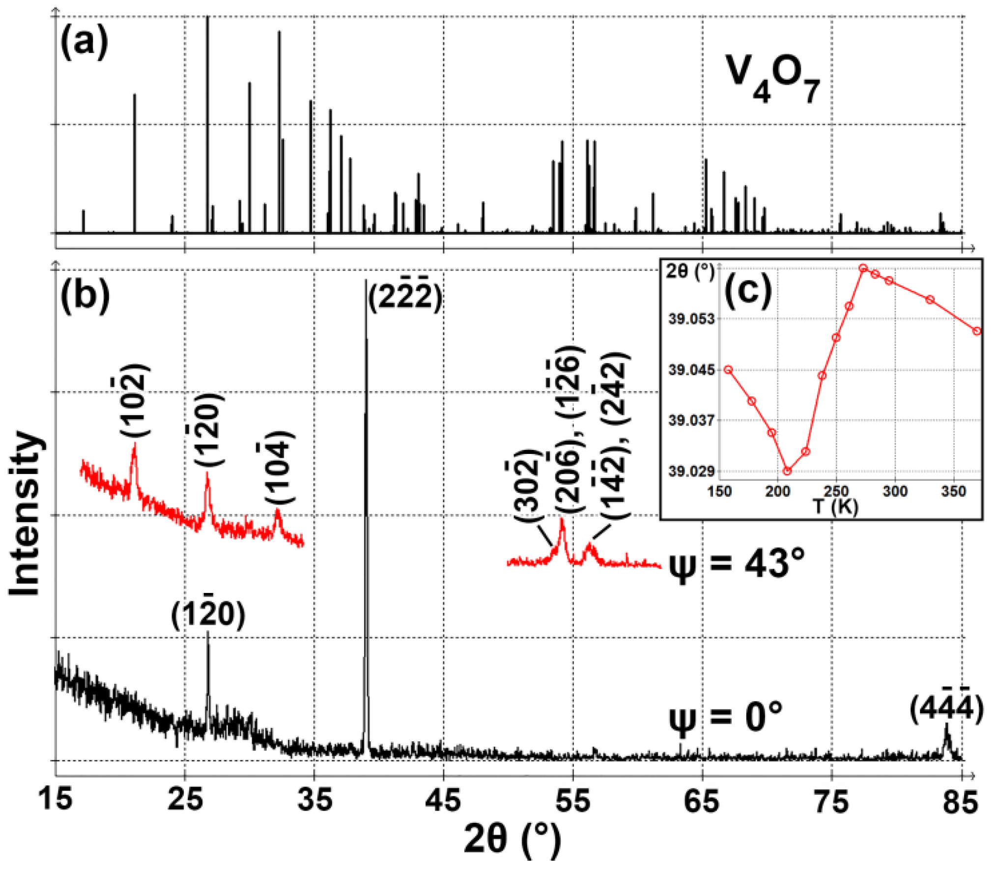
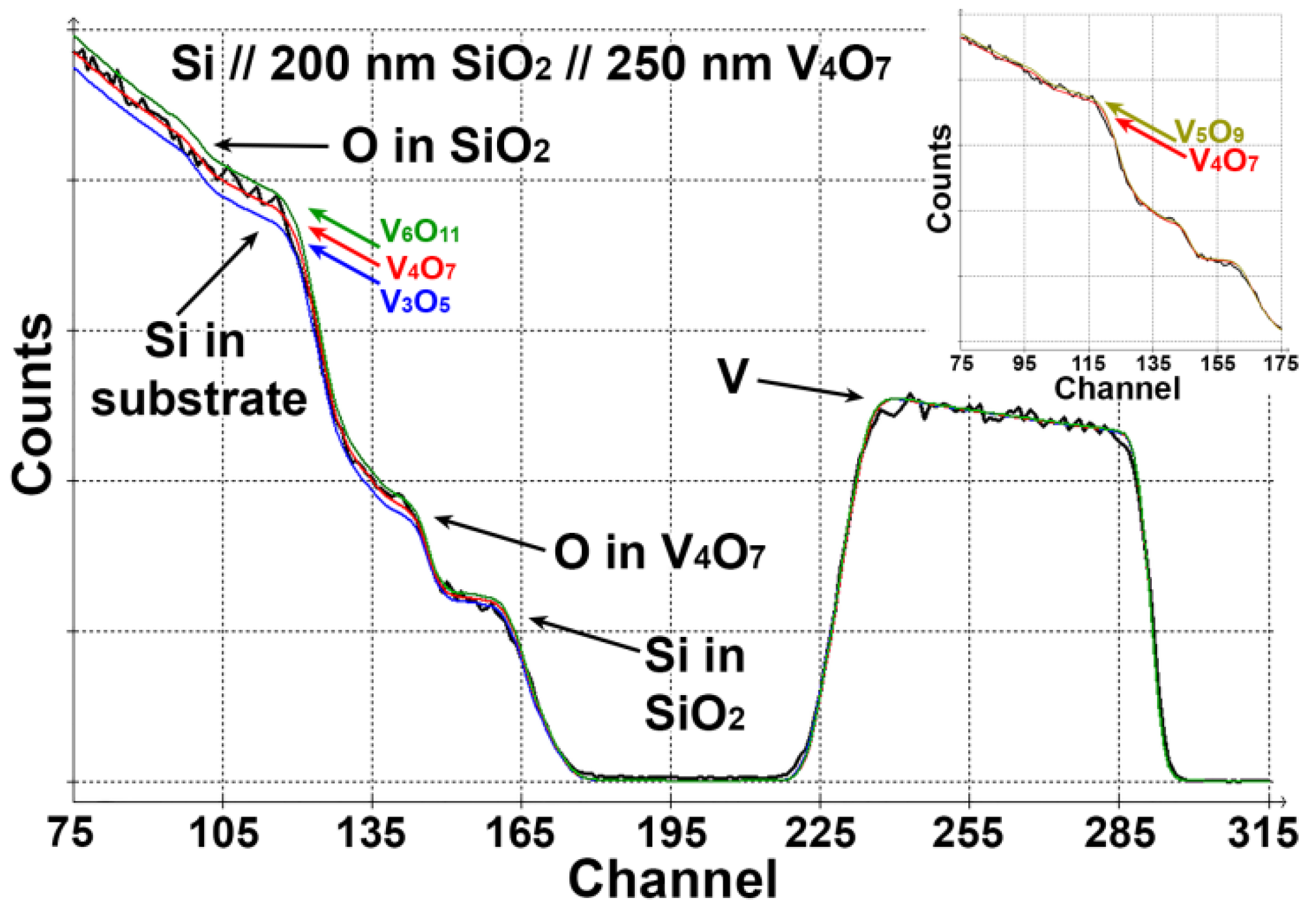
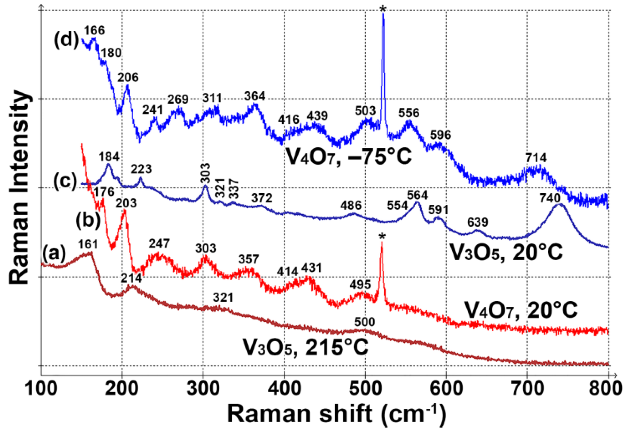
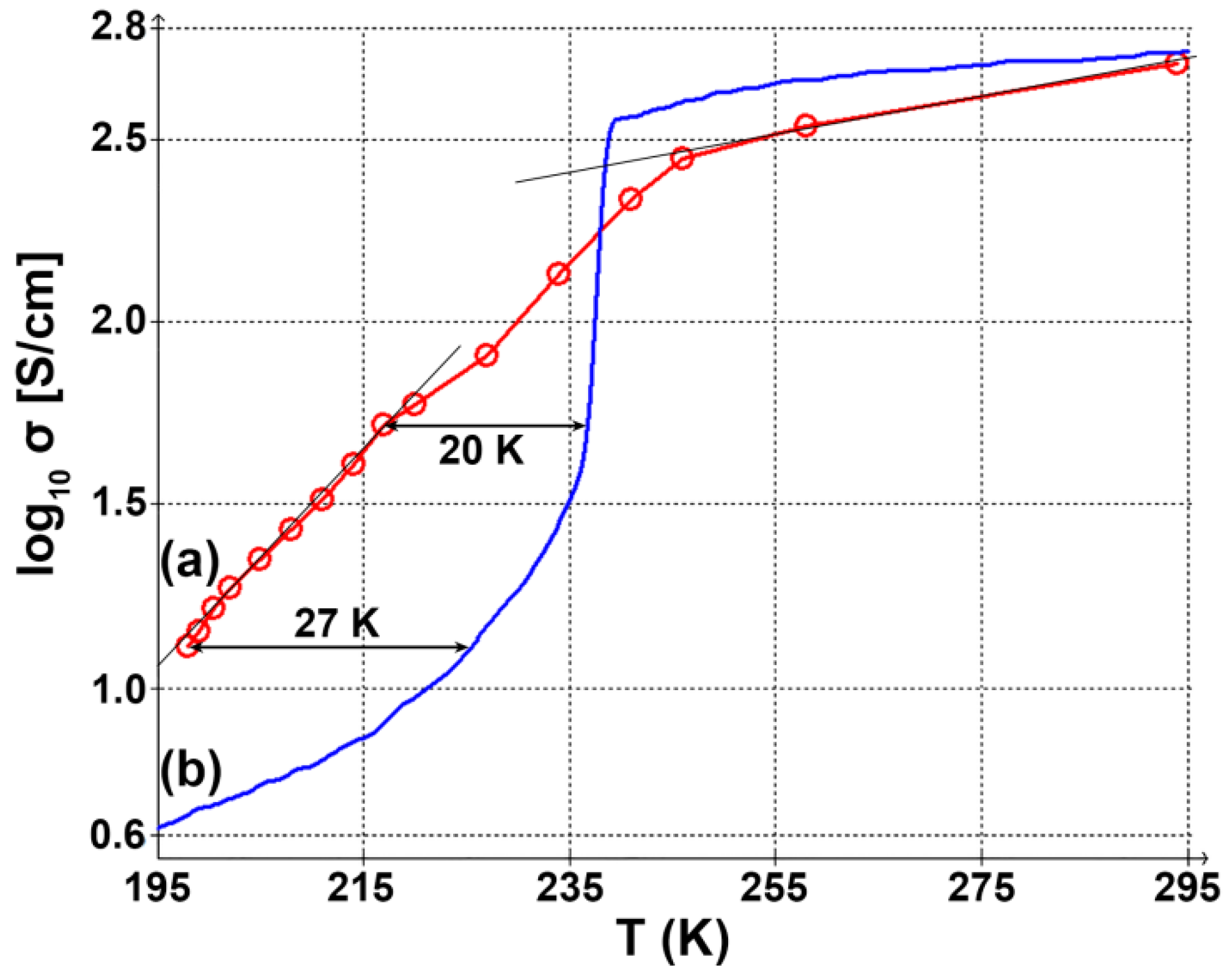
3. Results and Discussion

XRD pattern for a powder V4O7 sample was calculated based on the crystal structure from ref. [5] using Profex software [15] (Figure 1a). Our V4O7 film (Figure 1b) is highly textured, and the only strong peak is located at 2θ = 39.04°. The nearest reflection for the bulk sample is ( 2 22 ¯ ) at 2θ = 38.86°, so the compressive stress in the film is about 0.4%. A ( 2 22 ¯ ) reflection may be rewritten in rutile VO2 (R) subcell coordinates as (200)R [5]. Such texturing is typical for VO2 films [16,17], including samples produced by arc sputtering [18].
One of the characteristic reflections of V4O7 is ( 10 2 ¯ ) at 2θ = 21.14° (for V5O9 the equivalent reflection is ( 10 2 ¯ ) at 2θ = 22.36° [19] and for V3O5 the equivalent reflection is (200) at 2θ = 19.13° [20]). For a sample with a texture of ( 2 22 ¯ ), this reflection can be observed in θ–2θ scans if a sample tilt of ψ = 43° is applied (this angle is calculated according to ref. [21]). In Figure 1b we indeed see such a reflection at 2θ = 21.13°, confirming the formation of V4O7. The experimental configuration at ψ = 43° supports the observation of several other expected reflections: ( 1 2 ¯ 0 ) at 2θ = 26.81° (expected at 2θ = 26.76°, ψ = 32°), ( 10 4 ¯ ) at 2θ = 32.22° (expected at 2θ = 32.3°, ψ = 49°), ( 30 2 ¯ ) at 2θ = 53.6° (expected at 2θ = 53.45°, ψ = 45°), ( 20 6 ¯ ) or ( 1 26 ¯ ) at 2θ = 54.2° (expected at 2θ = 53.96°, ψ = 45° or 2θ = 54.16°, ψ = 43°, respectively), ( 1 42 ¯ ) at 2θ = 56.25° (expected at 2θ = 56.13°, ψ = 43°) and ( 2 4 ¯ 2 ) at 2θ = 56.7° (expected at 2θ = 56.63°, ψ = 43°). Since we observe all the expected peaks (with relatively high intensities) and only the expected reflections, we can conclude that our film is indeed V4O7 and contains no other phases.
Temperature dependence of the position of ( 2 22 ¯ ) reflection is shown in Figure 1c. We can see the abnormal expansion of the lattice during the sample cooling from 0 to −65 °C. Such behavior is associated with the phase transition in V4O7. However, the discontinuity on the graph, which could help to locate the exact transition temperature, can hardly be seen even for single crystals [5]. For thin films, the phase transition is usually not abrupt, which is related to the complex internal strain dynamics in the film [7,22]. Thus, we can only conclude that the phase transition temperature in our sample is above −65 °C.
The formation of V4O7 is further confirmed by elemental analysis performed by RBS (Figure 2). An experimental spectrum was fitted, suggesting structures with different values of x in the VOx layer. The number of incident particles was adjusted to minimize the quadratic deviation for the signal from vanadium (channels 245–280). Then, the value of the reduced quadratic deviation χ R 2 was analyzed for the oxygen region (channels 75–115). The film composition of V4O7 gives the best agreement between experiment and simulation ( χ R 2 = 1.4). The accuracy of the method rules out the formation of V3O5 or Magnéli phases with n ≥ 6 ( χ R 2 = 8.6 and 5.3 for V3O5 and V6O11, respectively). However, it would be challenging to distinguish between V4O7 and V5O9, since V5O9 also gives an acceptable agreement between experiment and simulation ( χ R 2 = 2.3).
Morphology of V4O7 film was investigated using SEM and AFM (Figure 3). From the Scherrer equation (FWHM of ( 2 22 ¯ ) peak is 0.15°), we can estimate the average crystallite size as 60 nm. This value is consistent with visible grain sizes (Figure 3a,b,d). Additionally, using a watershed algorithm, we determined that the distribution of equivalent disk diameter for grains has a maximum of 60 nm and a mean value of 100 nm. From the cross-section image (Figure 3c), we can estimate the film thickness as 240 nm, which is in good agreement with the value obtained by RBS.
Raman spectrum of V4O7 film is shown in Figure 4. The spectrum is similar to one observed in our previous work (VOx, Figure 12 in ref. [6]). However, this VOx phase was not properly identified, and the sample contained impurities. V4O7 undergoes a phase transition between −36 and −23 °C, so two different spectra are presented: above (20 °C, Figure 4b) and below (−75 °C, Figure 4d) the phase transition temperature. Cooling the V4O7 sample leads to a blueshift of all Raman bands. Moreover, low-temperature modification has four additional peaks at 166, 556, 596 and 714 cm−1. Such spectral changes can be compared with the behavior of another Magnéli phase, V3O5 (Figure 4a,c). Similarly to V4O7, heating of V3O5 above the phase transition leads to the disappearance of strong peaks at higher wavenumbers: 564, 591 and 740 cm−1.
Temperature-dependent Raman measurements are summarized in Figure 5. Only slight blueshifts of the bands are observed up to −50 °C. At −55 °C, we can see the appearance of new peaks at 165, 553, 593 and 709 cm−1. Further cooling does not significantly influence the spectrum. The spectral changes are fully reversible if the sample is heated to room temperature after the cooling. From our measurements, we can conclude that the sample undergoes a phase transition at a temperature between −50 and −55 °C. This temperature is slightly lower than the phase transition temperature of bulk V4O7 (the reported values are −36 [4] or −23 °C [5]). The discrepancy can be explained by the effect of external surface and grain-boundary surface energies [23]. This effect shifts the phase transition temperature by up to several tens of degrees to lower or higher values and is typical for thin films. Note that the phase transition in other Magnéli phases occurs at much lower temperatures (the highest one is about −100 °C for V6O11 [3]).
Temperature dependence of the V4O7 film electrical conductivity is given in Figure 6. Similar to XRD, we can see a broad transition region between −25 and −55 °C. The absolute value of conductivity at room temperature agrees well with the value previously reported for the bulk crystal [4]. For the low-temperature region, our curve is shifted by 20–25 K. Such shift is consistent with our observations derived from Raman spectroscopy.

4. Conclusions

Magnéli phases of vanadium oxides were directly produced by a sputtering technique. During the cathodic arc sputtering of the vanadium target, V4O7 grows by 17 nm/min at 600 °C and 0.045 Pa of oxygen pressure. Produced V4O7 films have a preferred orientation of ( 2 22 ¯ ) corresponding to (200) in rutile coordinates. The stoichiometry of V4O7 was confirmed by Rutherford backscatter spectrometry. The room temperature Raman spectrum of this phase is relatively weak, and its measurement requires careful tuning of the laser power on the sample. The spectrum consists of one strong narrow peak at 203 cm−1 and several weaker and broader bands at 176, 247, 303, 357, 414, 431 and 495 cm−1. Metal–insulator phase transition in V4O7 was observed by Raman spectroscopy between −50 and −55 °C. The low-temperature spectrum is characterized by four additional bands at 166, 556, 596 and 714 cm−1 (at −75 °C).

Author Contributions

Conceptualization, P.S. and K.M.; Data curation, P.S.; Formal analysis, P.S.; Funding acquisition, A.G.; Investigation, P.S.; Methodology, P.S.; Project administration, A.G.; Resources, P.S.; Software, P.S.; Supervision, K.M.; Validation, P.S., K.M. and A.G.; Visualization, P.S.; Writing—Original Draft, P.S.; Writing—Review and Editing, K.M. and A.G. All authors have read and agreed to the published version of the manuscript.

Funding

This research was funded by Ministry of Science and Higher Education of the Russian Federation, Grant No. FZWM-2020-0008.

Institutional Review Board Statement

Not applicable.

Informed Consent Statement

Not applicable.

Data Availability Statement

Data are contained within the article.

Acknowledgments

We are grateful to Ivan Lyatun for performing SEM measurements. We are also grateful to Olga Dikaya for the help with AFM data processing.

Conflicts of Interest

The authors declare no conflict of interest. The funders had no role in the design of the study; in the collection, analyses, or interpretation of data; in the writing of the manuscript, or in the decision to publish the results.

References

  1. Andersson, G. Studies on vanadium oxides. I. phase analysis. Acta Chem. Scand. 1954, 8, 1599–1606. [Google Scholar] [CrossRef] [Green Version]
  2. Horiuchi, H.; Tokonami, M.; Morimoto, N.; Nagasawa, K.; Bando, Y.; Takada, T. Crystallography of VnO2n−1 (3 ≤ n ≤ 8). Mater. Res. Bull. 1971, 6, 833–843. [Google Scholar] [CrossRef]
  3. Kachi, S.; Kosuge, K.; Okinaka, H. Metal-insulator transition in VnO2n−1. J. Solid State Chem. 1973, 6, 258–270. [Google Scholar] [CrossRef]
  4. Andreev, V.N.; Klimov, V.A. Specific features of the electrical conductivity of V4O7 single crystals. Phys. Solid State 2009, 51, 2235. [Google Scholar] [CrossRef]
  5. Marezio, M.; McWhan, D.B.; Dernier, P.D.; Remeika, J.P. Structural aspects of the metal-insulator transition in V4O7. J. Solid State Chem. 1973, 6, 419–429. [Google Scholar] [CrossRef]
  6. Shvets, P.; Dikaya, O.; Maksimova, K.; Goikhman, A. A review of Raman spectroscopy of vanadium oxides. J. Raman Spectrosc. 2019, 50, 1226–1244. [Google Scholar] [CrossRef]
  7. Lysenko, S.; Rúa, A.; Kumar, N.; Lu, J.; Yan, J.-A.; Theran, L.; Echeverria, K.; Ramos, L.; Goenaga, G.; Hernández-Rivera, S.P.; et al. Raman spectra and elastic light scattering dynamics of V3O5 across insulator–metal transition. J. Appl. Phys. 2021, 129, 025111. [Google Scholar] [CrossRef]
  8. Al-Alharbi, L.; Alrooqi, A.; Ibrahim, M.M.; El-Mehasseb, I.M.; Kumeria, T.; Gobouri, A.; Altalhi, T.; El-Sheshtawy, H.S. In situ H2O2 generation for tuning reactivity of V4O7 nanoflakes and V2O5 nanorods for oxidase enzyme mimic activity and removal of organic pollutants. J. Environ. Chem. Eng. 2021, 9, 105044. [Google Scholar] [CrossRef]
  9. Nasr, M.; Gomaa, H.M.; Yahia, I.S.; Saleh, H.A. Novel thermochromic (TC) and electrochromic (EC) characteristics of the V4O7 liquid crystal for LCDs and versatile optoelectronic applications. J. Mol. Liq. 2021, 330, 115620. [Google Scholar] [CrossRef]
  10. Xu, J.; Hu, C.; Han, H.; He, M.; Wan, B.; Xia, C. The synthesis and photoelectric response of single-crystalline V4O7 nanowires. In Proceedings of the 2010 3rd International Nanoelectronics Conference, Hong Kong, China, 3–8 January 2010; pp. 413–414. [Google Scholar] [CrossRef]
  11. Wang, X.; Zheng, S.; Mu, X.; Zhang, Y.; Du, H. Additive-free synthesis of V4O7 hierarchical structures as high performance cathodes for lithium ion batteries. Chem. Commun. 2014, 50, 6775–6778. [Google Scholar] [CrossRef]
  12. Demeter, M.; Neumann, M.; Reichelt, W. Mixed-valence vanadium oxides studied by XPS. Surf. Sci. 2000, 454–456, 41–44. [Google Scholar] [CrossRef]
  13. Razavi, A.; Hughes, T.; Antinovitch, J.; Hoffman, J. Temperature effects on structure and optical properties of radio-frequency sputtered VO2. J. Vac. Sci. Technol. A 1989, 7, 1310–1313. [Google Scholar] [CrossRef]
  14. Mayer, M. SIMNRA, a simulation program for the analysis of NRA, RBS and ERDA. AIP Conf. Proc. 1999, 475, 541–544. [Google Scholar] [CrossRef]
  15. Doebelin, N.; Kleeberg, R. Profex: A graphical user interface for the Rietveld refinement program BGMN. J. Appl. Cryst. 2015, 48, 1573–1580. [Google Scholar] [CrossRef] [Green Version]
  16. Azhan, N.H.; Su, K.; Okimura, K.; Zaghrioui, M.; Sakai, J. Appearance of large crystalline domains in VO2 films grown on sapphire (001) and their phase transition characteristics. J. Appl. Phys. 2015, 117, 245314. [Google Scholar] [CrossRef]
  17. Ureña-Begara, F.; Crunteanu, A.; Raskin, J.-P. Raman and XPS characterization of vanadium oxide thin films with temperature. Appl. Surf. Sci. 2017, 403, 717–727. [Google Scholar] [CrossRef]
  18. Shvets, P.; Maksimova, K.; Goikhman, A. Polarized Raman scattering in micrometer-sized crystals of triclinic vanadium dioxide. J. Appl. Phys. 2021, 129, 055302. [Google Scholar] [CrossRef]
  19. Marezio, M.; Dernier, P.D.; McWhan, D.B.; Kachi, S. Structural aspects of the metal-insulator transition in V5O9. J. Solid State Chem. 1974, 11, 301–313. [Google Scholar] [CrossRef]
  20. Åsbrink, S. The crystal structure of and valency distribution in the low-temperature modification of V3O5. The decisive importance of a few very weak reflexions in a crystal-structure determination. Acta Cryst. 1980, B36, 1332–1339. [Google Scholar] [CrossRef]
  21. Suh, T.; Kang, S.O.; Suh, I.-H. InterplanarA: A computer program for the calculation of the crystallographic interplanar angles. Korean J. Crystallogr. 2009, 20, 15–18. [Google Scholar]
  22. Lee, D.; Lee, J.; Song, K.; Xue, F.; Choi, S.-Y.; Ma, Y.; Podkaminer, J.; Liu, D.; Liu, S.-C.; Chung, B.; et al. Sharpened VO2 phase transition via controlled release of epitaxial strain. Nano Lett. 2017, 17, 5614–5619. [Google Scholar] [CrossRef] [PubMed]
  23. Damodara Das, V.; Karunakaran, D. Thickness dependence of the phase transition temperature in Ag2Se thin films. J. Appl. Phys. 1990, 68, 2105–2111. [Google Scholar] [CrossRef]
Figure 1. (a) Calculated XRD powder pattern of V4O7. (b) XRD patterns of a V4O7 film measured at different sample tilts (ψ). (c) Dependence of ( 2 22 ¯ ) peak position on temperature.
Coatings 12 00291 g001
Figure 2. RBS of V4O7 film. Three color lines correspond to fits for films with different stoichiometry. Inset shows the comparison between experiment and simulation for V4O7 and V5O9. 1 channel = 3.94 keV.
Coatings 12 00291 g002
Figure 3. Morphology of V4O7 film. (a) SEM and (b) AFM images of the sample surface. (c) SEM image of the sample cross-section. (d) Height profile measured by AFM along the white line 1 in (b).
Coatings 12 00291 g003
Figure 4. Raman spectra of vanadium oxide Magnéli phases: (a) V3O5, high-temperature modification, (b) V4O7, high-temperature modification, (c) V3O5, low-temperature modification, (d) V4O7, low-temperature modification. The asterisk marks the position of the Si substrate peak.
Coatings 12 00291 g004
Figure 5. Raman spectra of V4O7 at different temperatures: (a) 20 °C, (b) –40 °C, (c) –50 °C, (d) –55 °C, (e) –60 °C, (f) –75 °C, (g) 20 °C after low-temperature measurements. The asterisk marks the position of the Si substrate peak. Arrows mark the appearance of new peaks indicating the phase transition.
Coatings 12 00291 g005
Figure 6. Temperature dependence of electrical conductivity (logarithmic scale). (a) V4O7 film, (b) V4O7 single crystal (data from [4]).
Coatings 12 00291 g006
Publisher’s Note: MDPI stays neutral with regard to jurisdictional claims in published maps and institutional affiliations.

