Carbon Dots as a Sustainable New Platform for Organic Light Emitting Diode


Abstract
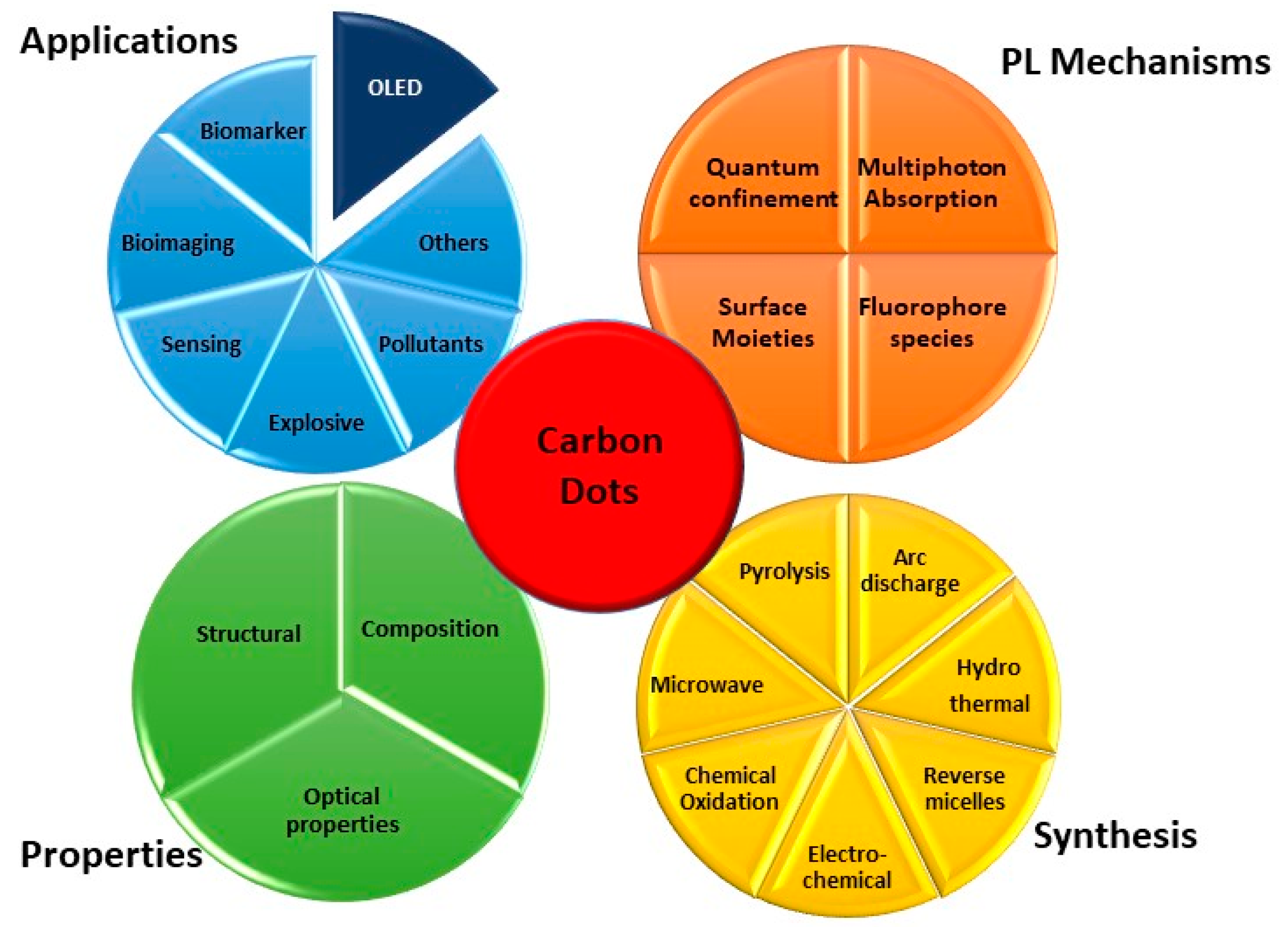
1. Introduction

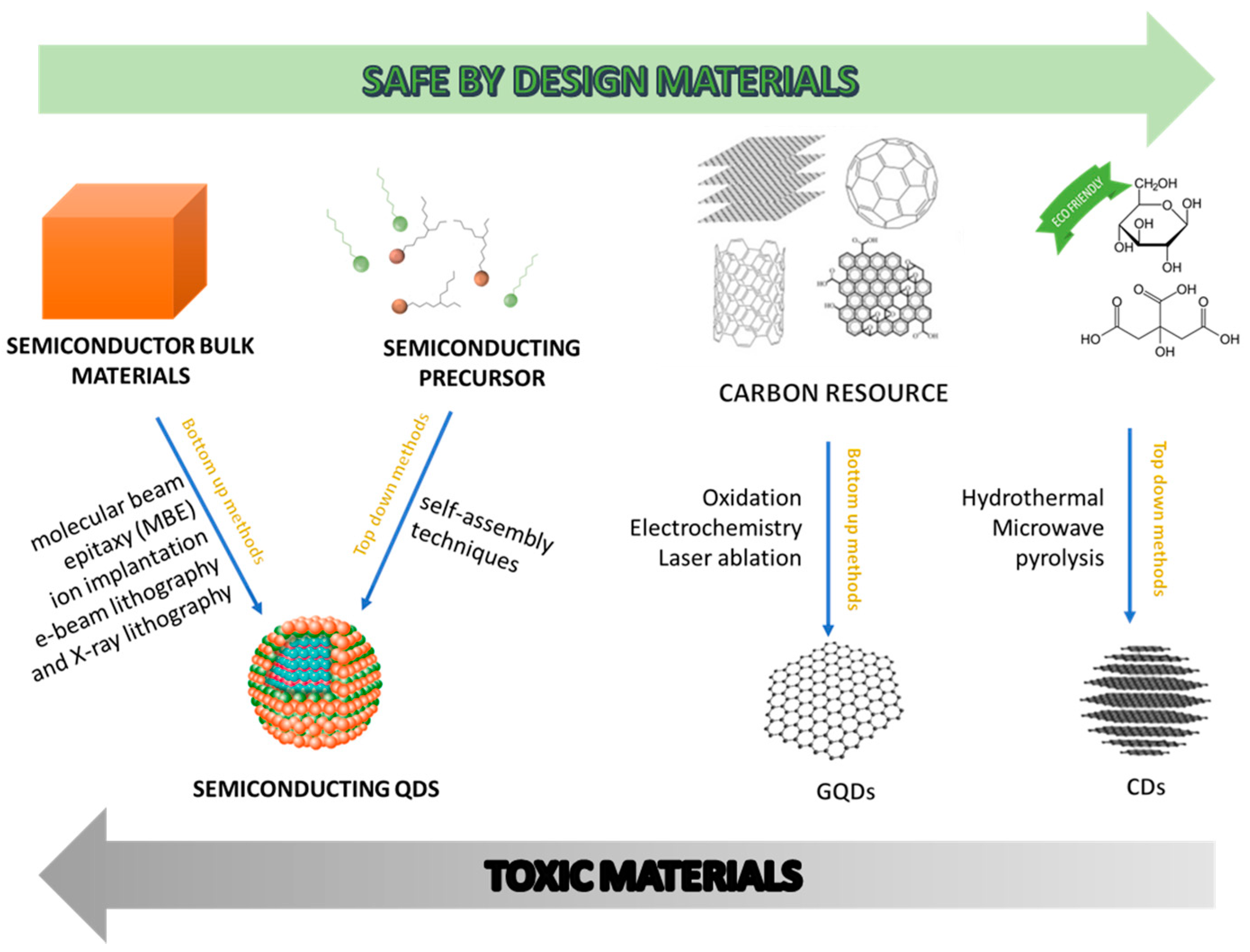
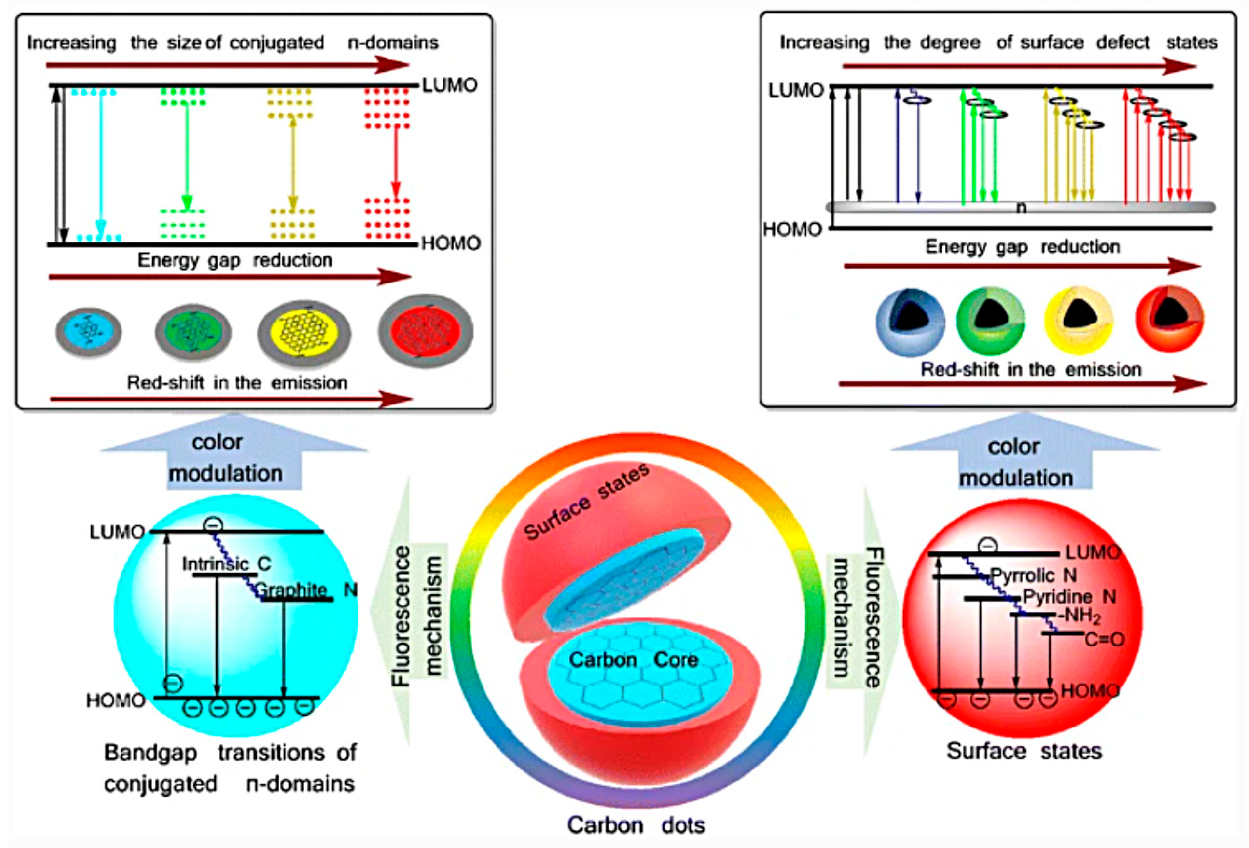
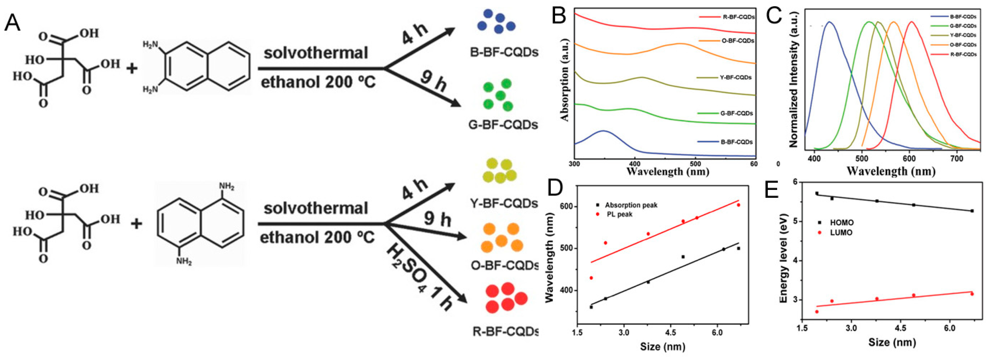
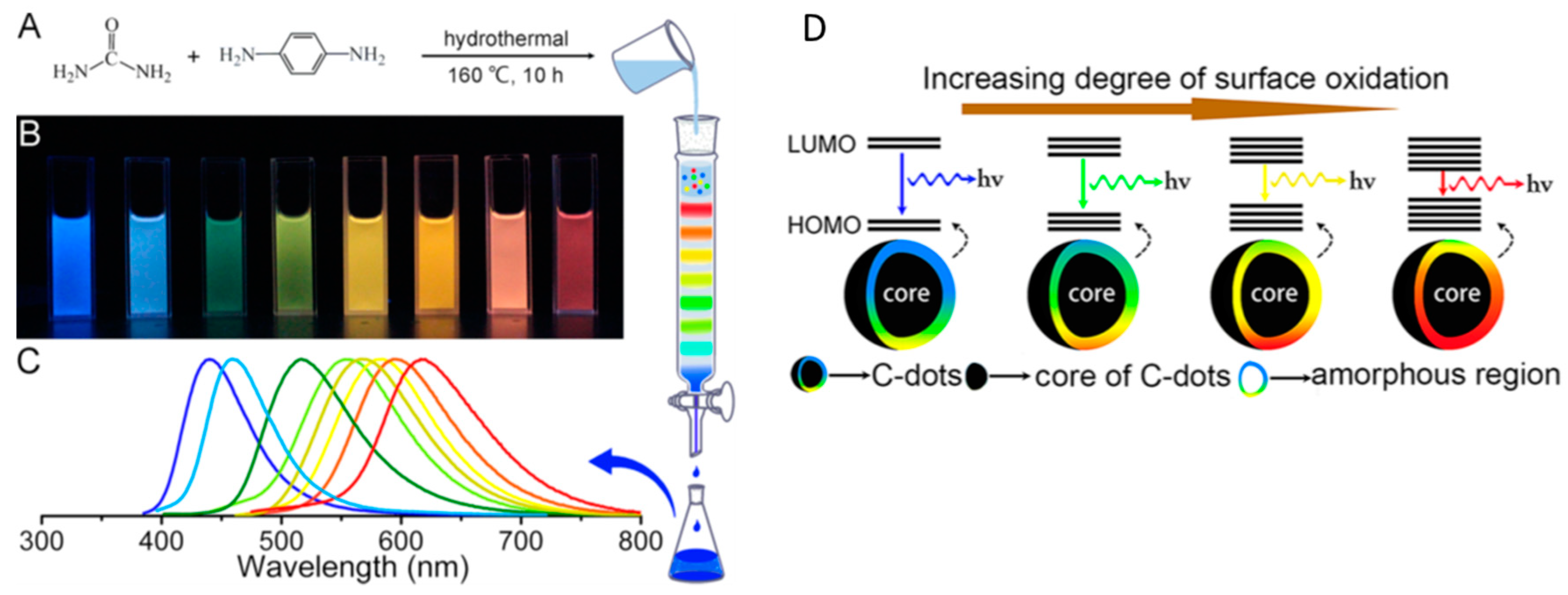
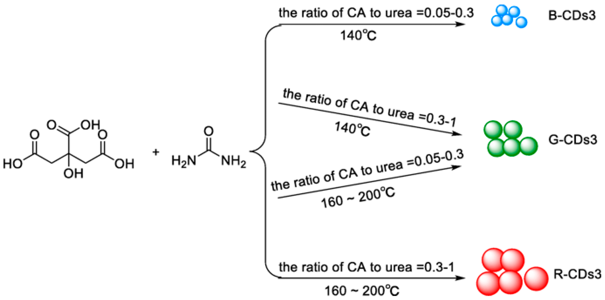
2. Definition of Carbon Dots and Optical Properties


3. OLED-Based Carbon Dots
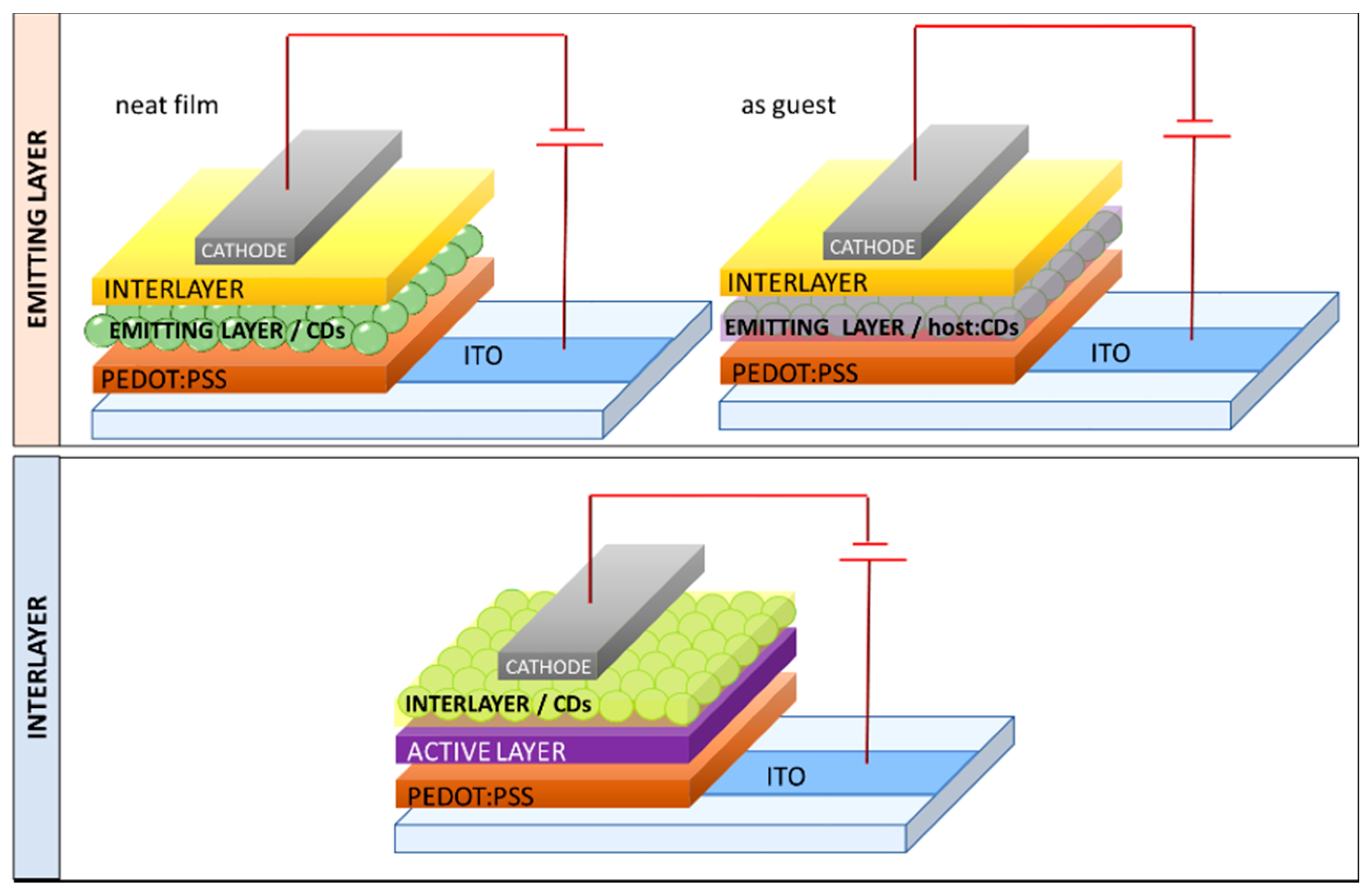
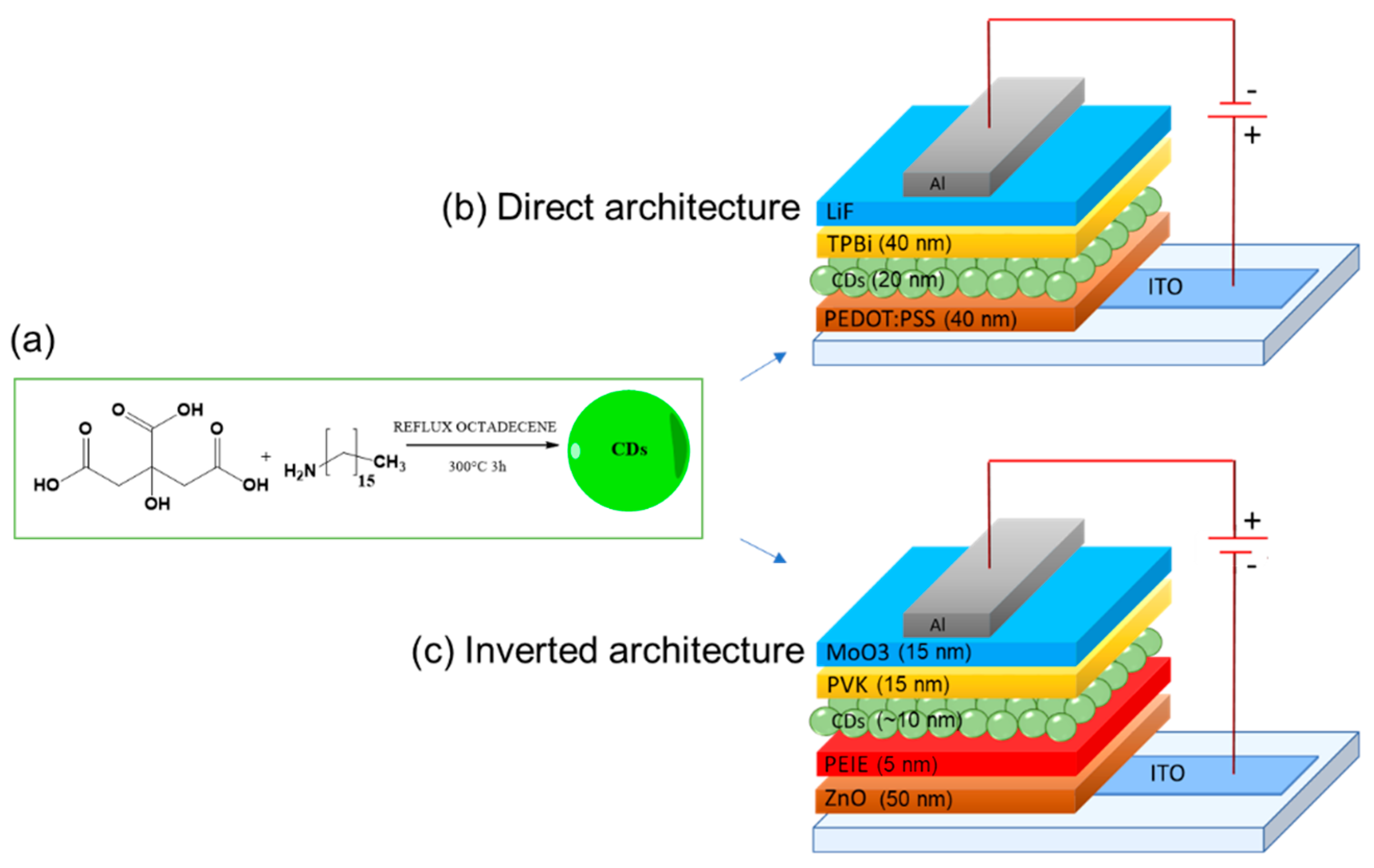
3.1. CDs as Emitter
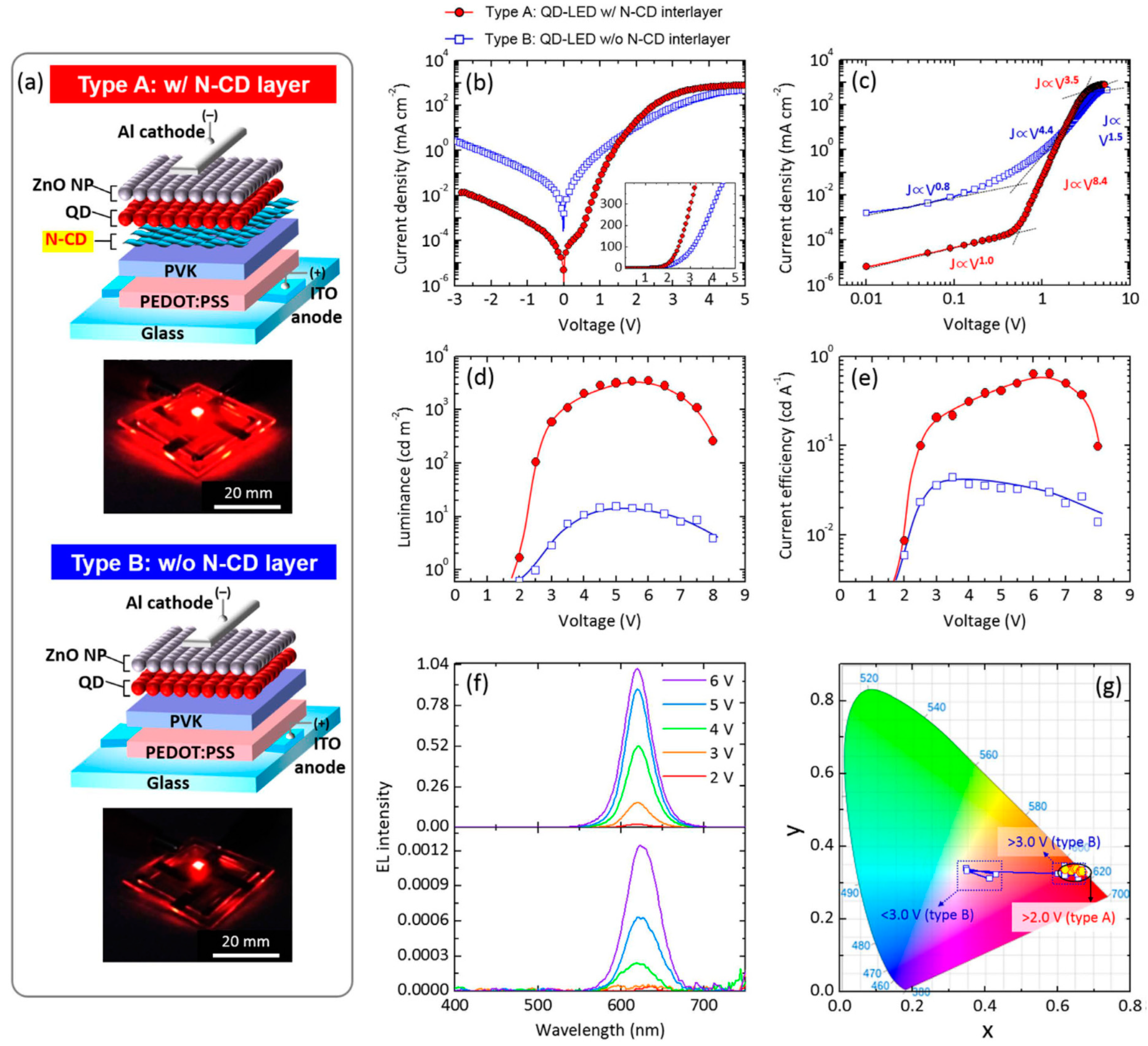
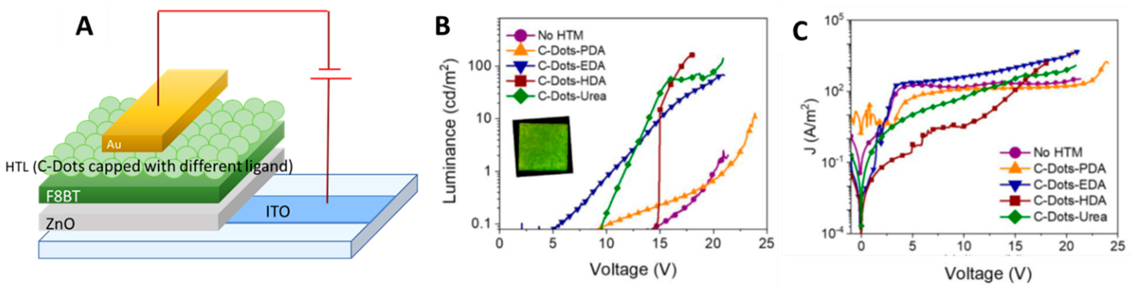
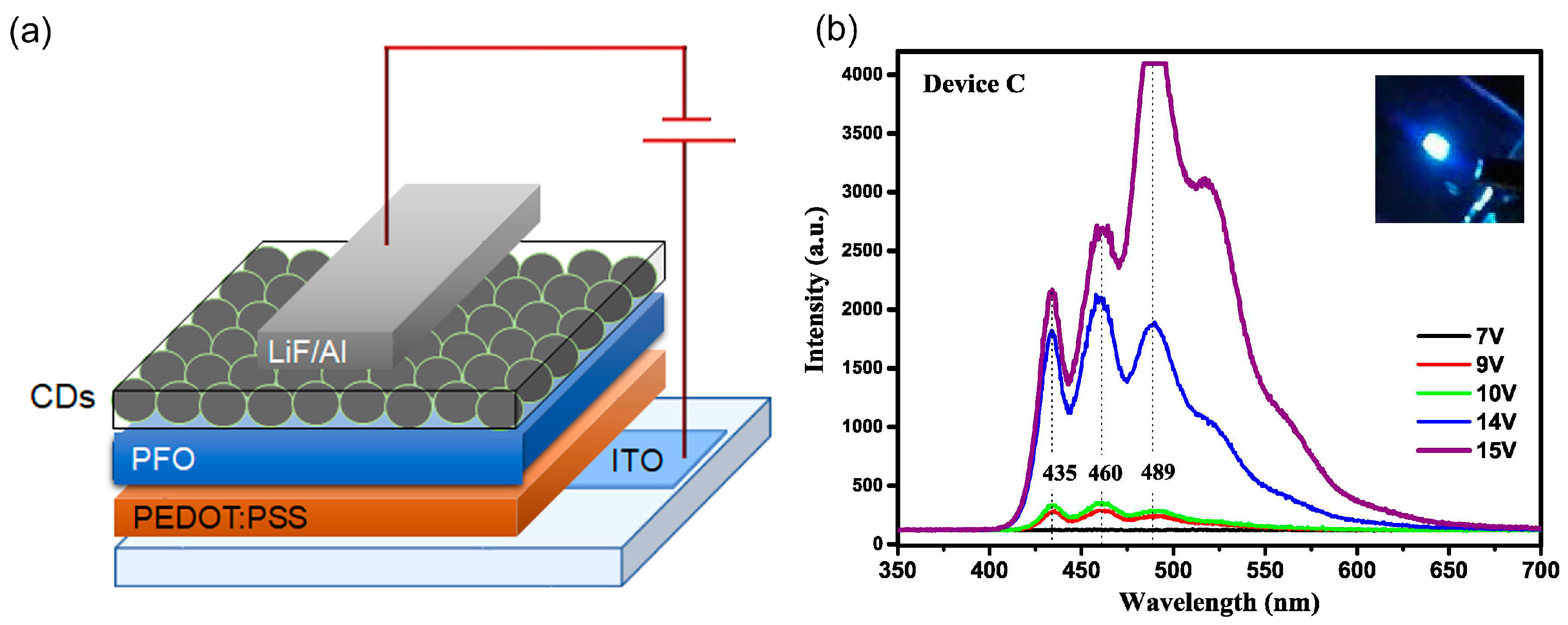
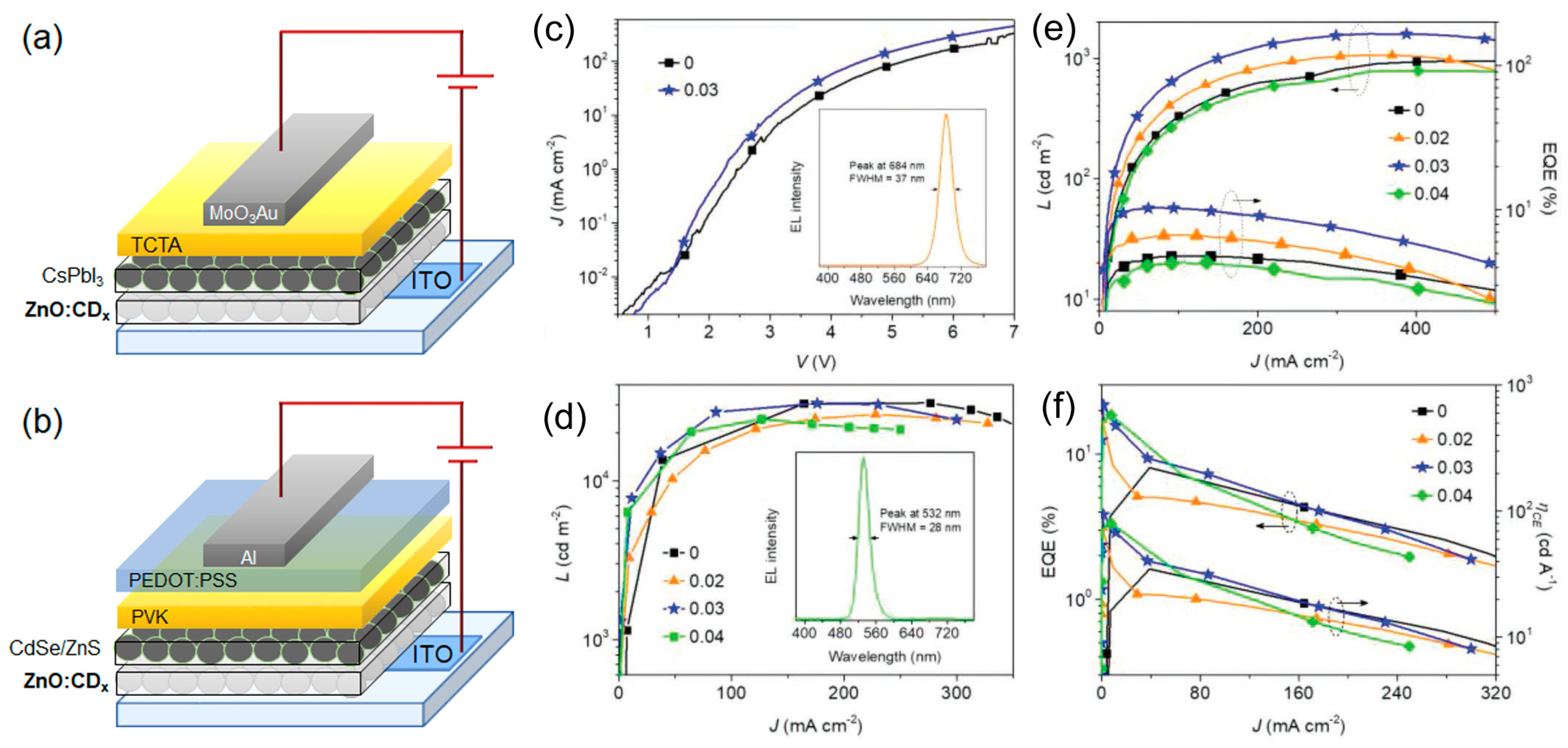
3.2. CDs as Charge Regulating Interlayer
4. Summary and Outlook
Author Contributions
Funding
Conflicts of Interest
References
- Baldé, C.P.; Forti, V.; Gray, V.; Kuehr, R.; Stegmann, P.; International Telecommunication Union; United Nations University; International Solid Waste Association. The Global E-Waste Monitor 2017: Quantities, Flows, and Resources; United Nations University: Tokyo, Japan; International Telecommunication Union: Geneva, Switzerland; International Solid Waste Association: Rotterdam, The Netherlands, 2017; ISBN 9789280890532. [Google Scholar]
- Ostroverkhova, O. Organic Optoelectronic Materials: Mechanisms and Applications. Chem. Rev. 2016, 116, 13279–13412. [Google Scholar] [CrossRef]
- Forrest, S.R.; Thompson, M.E. Introduction: Organic electronics and optoelectronics. Chem. Rev. 2007, 107, 923–925. [Google Scholar] [CrossRef]
- Hadziioannou, G.; Malliaras, G.G.M. Semiconducting Polymers: Chemistry, Physics and Engineering, 2nd Edition, Two-Volume Set; Hadziioannou, G., Malliaras, G.G.M., Eds.; Wiley: Hoboken, NJ, USA, 2006; ISBN 978-3-527-31271-9. [Google Scholar]
- Zvezdin, A.; Di Mauro, E.; Rho, D.; Santato, C.; Khalil, M. En route toward sustainable organic electronics. MRS Energy Sustain. 2020, 7. [Google Scholar] [CrossRef]
- Giovanella, U.; Betti, P.; Bolognesi, A.; Destri, S.; Melucci, M.; Pasini, M.; Porzio, W.; Botta, C. Core-type polyfluorene-based copolymers for low-cost light-emitting technologies. Org. Electron. 2010, 11, 2012–2018. [Google Scholar] [CrossRef]
- Irimia-Vladu, M. “Green” electronics: Biodegradable and biocompatible materials and devices for sustainable future. Chem. Soc. Rev. 2014, 43, 588–610. [Google Scholar] [CrossRef]
- Yan, L.; Zhao, F.; Wang, J.; Zu, Y.; Gu, Z.; Zhao, Y. A Safe-by-Design Strategy towards Safer Nanomaterials in Nanomedicines. Adv. Mater. 2019, 31, 1805391. [Google Scholar] [CrossRef]
- Gomulya, W.; Derenskyi, V.; Kozma, E.; Pasini, M.; Loi, M.A. Polyazines and polyazomethines with didodecylthiophene units for selective dispersion of semiconducting single-walled carbon nanotubes. Adv. Funct. Mater. 2015, 25, 5858–5864. [Google Scholar] [CrossRef]
- Xu, X.; Ray, R.; Gu, Y.; Ploehn, H.J.; Gearheart, L.; Raker, K.; Scrivens, W.A. Electrophoretic analysis and purification of fluorescent single-walled carbon nanotube fragments. J. Am. Chem. Soc. 2004, 126, 12736–12737. [Google Scholar] [CrossRef]
- Sun, Y.P.; Zhou, B.; Lin, Y.; Wang, W.; Fernando, K.A.S.; Pathak, P.; Meziani, M.J.; Harruff, B.A.; Wang, X.; Wang, H.; et al. Quantum-sized carbon dots for bright and colorful photoluminescence. J. Am. Chem. Soc. 2006, 128, 7756–7757. [Google Scholar] [CrossRef]
- Xiao, L.; Sun, H. Novel properties and applications of carbon nanodots. Nanoscale Horiz. 2018, 3, 565–597. [Google Scholar] [CrossRef]
- Li, X.; Rui, M.; Song, J.; Shen, Z.; Zeng, H. Carbon and graphene quantum dots for optoelectronic and energy devices: A review. Adv. Funct. Mater. 2015, 25, 4929–4947. [Google Scholar] [CrossRef]
- Semeniuk, M.; Yi, Z.; Poursorkhabi, V.; Tjong, J.; Jaffer, S.; Lu, Z.H.; Sain, M. Future perspectives and review on organic carbon dots in electronic applications. ACS Nano 2019, 13, 6224–6255. [Google Scholar] [CrossRef]
- Campuzano, S.; Yáñez-Sedeño, P.; Pingarrón, J.M. Carbon dots and graphene quantum dots in electrochemical biosensing. Nanomaterials 2019, 9, 634. [Google Scholar] [CrossRef]
- Liu, M.L.; Chen, B.B.; Li, C.M.; Huang, C.Z. Carbon dots: Synthesis, formation mechanism, fluorescence origin and sensing applications. Green Chem. 2019, 21, 449–471. [Google Scholar] [CrossRef]
- Wang, Y.; Hu, A. Carbon quantum dots: Synthesis, properties and applications. J. Mater. Chem. C 2014, 2, 6921–6939. [Google Scholar] [CrossRef]
- Gayen, B.; Palchoudhury, S.; Chowdhury, J. Carbon dots: A mystic star in the world of nanoscience. J. Nanomater. 2019, 2019, 3451307. [Google Scholar] [CrossRef]
- Chan, K.K.; Yap, S.H.K.; Yong, K.T. Biogreen synthesis of carbon dots for biotechnology and nanomedicine applications. Nano-Micro Lett. 2018, 10, 72. [Google Scholar] [CrossRef]
- Zuo, J.; Jiang, T.; Zhao, X.; Xiong, X.; Xiao, S.; Zhu, Z. Preparation and application of fluorescent carbon dots. J. Nanomater. 2015, 2015. [Google Scholar] [CrossRef]
- Pal, A.; Sk, M.P.; Chattopadhyay, A. Recent advances in crystalline carbon dots for superior application potential. Mater. Adv. 2020, 1, 525–553. [Google Scholar] [CrossRef]
- Wang, L.; Li, W.; Yin, L.; Liu, Y.; Guo, H.; Lai, J.; Han, Y.; Li, G.; Li, M.; Zhang, J.; et al. Full-color fluorescent carbon quantum dots. Sci. Adv. 2020, 6, eabb6772. [Google Scholar] [CrossRef] [PubMed]
- Li, X.; Wang, H.; Shimizu, Y.; Pyatenko, A.; Kawaguchi, K.; Koshizaki, N. Preparation of carbon quantum dots with tunable photoluminescence by rapid laser passivation in ordinary organic solvents. Chem. Commun. 2011, 47, 932–934. [Google Scholar] [CrossRef] [PubMed]
- Yang, Z.C.; Wang, M.; Yong, A.M.; Wong, S.Y.; Zhang, X.H.; Tan, H.; Chang, A.Y.; Li, X.; Wang, J. Intrinsically fluorescent carbon dots with tunable emission derived from hydrothermal treatment of glucose in the presence of monopotassium phosphate. Chem. Commun. 2011, 47, 11615–11617. [Google Scholar] [CrossRef] [PubMed]
- Hu, S.; Liu, J.; Yang, J.; Wang, Y.; Cao, S. Laser synthesis and size tailor of carbon quantum dots. J. Nanoparticle Res. 2011, 13, 7247–7252. [Google Scholar] [CrossRef]
- Tarasenka, N.; Stupak, A.; Tarasenko, N.; Chakrabarti, S.; Mariotti, D. Structure and optical properties of carbon nanoparticles generated by laser treatment of graphite in liquids. ChemPhysChem 2017, 18, 1074–1083. [Google Scholar] [CrossRef] [PubMed]
- De, B.; Karak, N. A green and facile approach for the synthesis of water soluble fluorescent carbon dots from banana juice. RSC Adv. 2013, 3, 8286–8290. [Google Scholar] [CrossRef]
- Zhu, S.; Meng, Q.; Wang, L.; Zhang, J.; Song, Y.; Jin, H.; Zhang, K.; Sun, H.; Wang, H.; Yang, B. Highly photoluminescent carbon dots for multicolor patterning, sensors, and bioimaging. Angew. Chemie Int. Ed. 2013, 52, 3953–3957. [Google Scholar] [CrossRef]
- Dong, Y.; Pang, H.; Yang, H.B.; Guo, C.; Shao, J.; Chi, Y.; Li, C.M.; Yu, T. Carbon-based dots co-doped with nitrogen and sulfur for high quantum yield and excitation-independent emission. Angew. Chemie Int. Ed. 2013, 52, 7800–7804. [Google Scholar] [CrossRef]
- Chen, Y.; Lian, H.; Wei, Y.; He, X.; Chen, Y.; Wang, B.; Zeng, Q.; Lin, J. Concentration-induced multi-colored emissions in carbon dots: Origination from triple fluorescent centers. Nanoscale 2018, 10, 6734–6743. [Google Scholar] [CrossRef]
- Ehrat, F.; Bhattacharyya, S.; Schneider, J.; Löf, A.; Wyrwich, R.; Rogach, A.L.; Stolarczyk, J.K.; Urban, A.S.; Feldmann, J. Tracking the source of carbon dot photoluminescence: Aromatic domains versus molecular fluorophores. Nano Lett. 2017, 17, 7710–7716. [Google Scholar] [CrossRef]
- Bao, L.; Liu, C.; Zhang, Z.L.; Pang, D.W. Photoluminescence-tunable carbon nanodots: Surface-state energy-gap tuning. Adv. Mater. 2015, 27, 1663–1667. [Google Scholar] [CrossRef]
- Zhang, J.; Su, Z.C.; Cui, Y.; Hu, G.; Tang, Y.L.; Gan, Z.X.; Yang, L.; Lao, X.Z.; Bao, Y.T.; Xu, S.J. The roles of self-absorption and radiative energy transfer in photoluminescence of N-doped carbon nanodots in solution. AIP Adv. 2019, 9, 035135. [Google Scholar] [CrossRef]
- Khan, S.; Gupta, A.; Verma, N.C.; Nandi, C.K. Time-resolved emission reveals ensemble of emissive states as the origin of multicolor fluorescence in carbon dots. Nano Lett. 2015, 15, 8300–8305. [Google Scholar] [CrossRef] [PubMed]
- Zhu, S.; Zhang, J.; Liu, X.; Li, B.; Wang, X.; Tang, S.; Meng, Q.; Li, Y.; Shi, C.; Hu, R.; et al. Graphene quantum dots with controllable surface oxidation, tunable fluorescence and up-conversion emission. RSC Adv. 2012, 2, 2717. [Google Scholar] [CrossRef]
- Wang, X.; Qu, K.; Xu, B.; Ren, J.; Qu, X. Microwave assisted one-step green synthesis of cell-permeable multicolor photoluminescent carbon dots without surface passivation reagents. J. Mater. Chem. 2011, 21, 2445. [Google Scholar] [CrossRef]
- Yang, S.T.; Wang, X.; Wang, H.; Lu, F.; Luo, P.G.; Cao, L.; Meziani, M.J.; Liu, J.H.; Liu, Y.; Chen, M.; et al. Carbon dots as nontoxic and high-performance fluorescence imaging agents. J. Phys. Chem. C 2009, 113, 18110–18114. [Google Scholar] [CrossRef] [PubMed]
- Wang, K.; Gao, Z.; Gao, G.; Wo, Y.; Wang, Y.; Shen, G.; Cui, D. Systematic safety evaluation on photoluminescent carbon dots. Nanoscale Res. Lett. 2013, 8, 1–9. [Google Scholar] [CrossRef]
- Dias, C.; Vasimalai, N.; Sárria, M.P.; Pinheiro, I.; Vilas-Boas, V.; Peixoto, J.; Espiña, B. Biocompatibility and bioimaging potential of fruit-based carbon dots. Nanomaterials 2019, 9, 199. [Google Scholar] [CrossRef]
- Sendão, R.; de Yuso, M.D.V.M.; Algarra, M.; da Silva, J.C.E.; da Silva, L.P. Comparative life cycle assessment of bottom-up synthesis routes for carbon dots derived from citric acid and urea. J. Clean. Prod. 2020, 254. [Google Scholar] [CrossRef]
- Zhu, S.; Song, Y.; Zhao, X.; Shao, J.; Zhang, J.; Yang, B. The photoluminescence mechanism in carbon dots (graphene quantum dots, carbon nanodots, and polymer dots): Current state and future perspective. Nano Res. 2015, 8, 355–381. [Google Scholar] [CrossRef]
- Giovanella, U.; Pasini, M.; Botta, C. Organic Light-Emitting Diodes (OLEDs): Working Principles and Device Technology; Springer: Cham, Switzerland, 2016; pp. 145–196. [Google Scholar]
- Squeo, B.M.; Pasini, M. BODIPY platform: A tunable tool for green to NIR OLEDs. Supramol. Chem. 2020, 32, 56–70. [Google Scholar] [CrossRef]
- De Medeiros, T.V.; Manioudakis, J.; Noun, F.; Macairan, J.R.; Victoria, F.; Naccache, R. Microwave-assisted synthesis of carbon dots and their applications. J. Mater. Chem. C 2019, 7, 7175–7195. [Google Scholar] [CrossRef]
- Huang, C.C.; Hung, Y.S.; Weng, Y.M.; Chen, W.; Lai, Y.S. Sustainable development of carbon nanodots technology: Natural products as a carbon source and applications to food safety. Trends Food Sci. Technol. 2019, 86, 144–152. [Google Scholar] [CrossRef]
- Ludmerczki, R.; Mura, S.; Carbonaro, C.M.; Mandity, I.M.; Carraro, M.; Senes, N.; Garroni, S.; Granozzi, G.; Calvillo, L.; Marras, S.; et al. Carbon dots from citric acid and its intermediates formed by thermal decomposition. Chem. A Eur. J. 2019, 25, 11963–11974. [Google Scholar] [CrossRef] [PubMed]
- Yuan, F.; Li, S.; Fan, Z.; Meng, X.; Fan, L.; Yang, S. Shining carbon dots: Synthesis and biomedical and optoelectronic applications. Nano Today 2016, 11. [Google Scholar] [CrossRef]
- Li, X.; Zhang, S.; Kulinich, S.A.; Liu, Y.; Zeng, H. Engineering surface states of carbon dots to achieve controllable luminescence for solid-luminescent composites and sensitive Be2+ detection. Sci. Rep. 2014, 4, 1–8. [Google Scholar] [CrossRef]
- Kandasamy, G. Recent advancements in doped/co-doped carbon quantum dots for multi-potential applications. C J. Carbon Res. 2019, 5, 24. [Google Scholar] [CrossRef]
- Mandal, B.; Sarkar, S.; Sarkar, P. Exploring the electronic structure of graphene quantum dots. J. Nanoparticle Res. 2012, 14. [Google Scholar] [CrossRef]
- Li, Y.; Shu, H.; Niu, X.; Wang, J. Electronic and optical properties of edge-functionalized graphene quantum dots and the underlying mechanism. J. Phys. Chem. C 2015, 119, 24950–24957. [Google Scholar] [CrossRef]
- Yamijala, S.S.; Bandyopadhyay, A.; Pati, S.K. Structural stability, electronic, magnetic, and optical properties of rectangular graphene and boron nitride quantum dots: Effects of size, substitution, and electric field. J. Phys. Chem. C 2013, 117, 23295–23304. [Google Scholar] [CrossRef]
- Güttinger, J.; Stampfer, C.; Frey, T.; Ihn, T.; Ensslin, K. Graphene quantum dots in perpendicular magnetic fields. Phys. Status Solidi 2009, 246, 2553–2557. [Google Scholar] [CrossRef]
- Li, X.; Lau, S.P.; Tang, L.; Ji, R.; Yang, P. Sulphur doping: A facile approach to tune the electronic structure and optical properties of graphene quantum dots. Nanoscale 2014, 6, 5323–5328. [Google Scholar] [CrossRef] [PubMed]
- Tao, S.; Zhu, S.; Feng, T.; Xia, C.; Song, Y.; Yang, B. The polymeric characteristics and photoluminescence mechanism in polymer carbon dots: A review. Mater. Today Chem. 2017, 6. [Google Scholar] [CrossRef]
- Guo, W.; Luo, Y.; Wei, K.; Gao, X. A cellular level biocompatibility and biosafety evaluation of mesoporous SiO2-based nanocomposite with lanthanum species. J. Mater. Sci. 2011, 47, 1514–1521. [Google Scholar] [CrossRef]
- Ge, J.; Lan, M.; Zhou, B.; Liu, W.; Guo, L.; Wang, H.; Jia, Q.; Niu, G.; Huang, X.; Zhou, H.; et al. A graphene quantum dot photodynamic therapy agent with high singlet oxygen generation. Nat. Commun. 2014, 5, 1–8. [Google Scholar] [CrossRef] [PubMed]
- Tang, L.; Ji, R.; Li, X.; Bai, G.; Liu, C.P.; Hao, J.; Lin, J.; Jiang, H.; Teng, K.S.; Yang, Z.; et al. Deep ultraviolet to near-infrared emission and photoresponse in layered n-doped graphene quantum dots. ACS Nano 2014, 8, 6312–6320. [Google Scholar] [CrossRef] [PubMed]
- Shamsipur, M.; Barati, A.; Karami, S. Long-wavelength, multicolor, and white-light emitting carbon-based dots: Achievements made, challenges remaining, and applications. Carbon N. Y. 2017, 124. [Google Scholar] [CrossRef]
- Song, Y.; Zhu, S.; Zhang, S.; Fu, Y.; Wang, L.; Zhao, X.; Yang, B. Investigation from chemical structure to photoluminescent mechanism: A type of carbon dots from the pyrolysis of citric acid and an amine. J. Mater. Chem. C 2015, 3, 5976–5984. [Google Scholar] [CrossRef]
- Wang, Y.; Li, Y.; Yan, Y.; Xu, J.; Guan, B.; Wang, Q.; Li, J.; Yu, J. Luminescent carbon dots in a new magnesium aluminophosphate zeolite. Chem. Commun. 2013, 49, 9006–9008. [Google Scholar] [CrossRef] [PubMed]
- Xu, Q.; Kuang, T.; Liu, Y.; Cai, L.; Peng, X.; Sreenivasan Sreeprasad, T.; Zhao, P.; Yu, Z.; Li, N. Heteroatom-doped carbon dots: Synthesis, characterization, properties, photoluminescence mechanism and biological applications. J. Mater. Chem. B 2016, 4, 7204–7219. [Google Scholar] [CrossRef] [PubMed]
- Li, L.; Dong, T. Photoluminescence tuning in carbon dots: Surface passivation or/and functionalization, heteroatom doping. J. Mater. Chem. C 2018, 6, 7944–7970. [Google Scholar] [CrossRef]
- Yan, F.; Sun, Z.; Zhang, H.; Sun, X.; Jiang, Y.; Bai, Z. The fluorescence mechanism of carbon dots, and methods for tuning their emission color: A review. Microchim. Acta 2019, 186, 583. [Google Scholar] [CrossRef] [PubMed]
- Yuan, F.; Wang, Z.; Li, X.; Li, Y.; Tan, Z.; Fan, L.; Yang, S. Bright multicolor bandgap fluorescent carbon quantum dots for electroluminescent light-emitting diodes. Adv. Mater. 2017, 29. [Google Scholar] [CrossRef] [PubMed]
- Ding, Y.; Zhang, F.; Xu, J.; Miao, Y.; Yang, Y.; Liu, X.; Xu, B. Synthesis of short-chain passivated carbon quantum dots as the light emitting layer towards electroluminescence. RSC Adv. 2017, 7, 28754–28762. [Google Scholar] [CrossRef]
- Miao, X.; Qu, D.; Yang, D.; Nie, B.; Zhao, Y.; Fan, H.; Sun, Z. Synthesis of carbon dots with multiple color emission by controlled graphitization and surface functionalization. Adv. Mater. 2018, 30, 1704740. [Google Scholar] [CrossRef]
- Shi, L.; Yang, J.H.; Zeng, H.B.; Chen, Y.M.; Yang, S.C.; Wu, C.; Zeng, H.; Yoshihito, O.; Zhang, Q. Carbon dots with high fluorescence quantum yield: The fluorescence originates from organic fluorophores. Nanoscale 2016, 8, 14374–14378. [Google Scholar] [CrossRef]
- Song, Y.; Zhu, S.; Yang, B. Bioimaging based on fluorescent carbon dots. RSC Adv. 2014, 4, 27184–27200. [Google Scholar] [CrossRef]
- Ding, H.; Yu, S.B.; Wei, J.S.; Xiong, H.M. Full-color light-emitting carbon dots with a surface-state-controlled luminescence mechanism. ACS Nano 2016, 10, 484–491. [Google Scholar] [CrossRef]
- Zheng, X.; Wang, H.; Gong, Q.; Zhang, L.; Cui, G.; Li, Q.; Chen, L.; Wu, F.; Wang, S. Highly luminescent carbon nanoparticles as yellow emission conversion phosphors. Mater. Lett. 2015, 143. [Google Scholar] [CrossRef]
- Joseph, J.; Anappara, A.A. White-light-emitting carbon dots prepared by the electrochemical exfoliation of graphite. ChemPhysChem 2017, 18, 292–298. [Google Scholar] [CrossRef]
- Wang, F.; Chen, Y.; Liu, C.; Ma, D. White light-emitting devices based on carbon dots’ electroluminescence. Chem. Commun. 2011, 47, 3502. [Google Scholar] [CrossRef]
- Paulo-Mirasol, S.; Martínez-Ferrero, E.; Palomares, E. Direct white light emission from carbon nanodots (C-dots) in solution processed light emitting diodes. Nanoscale 2019, 11, 11315–11321. [Google Scholar] [CrossRef] [PubMed]
- Zhang, X.; Zhang, Y.; Wang, Y.; Kalytchuk, S.; Kershaw, S.V.; Wang, Y.; Wang, P.; Zhang, T.; Zhao, Y.; Zhang, H.; et al. Color-switchable electroluminescence of carbon dot light-emitting diodes. ACS Nano 2013, 7, 11234–11241. [Google Scholar] [CrossRef] [PubMed]
- Xu, J.; Miao, Y.; Zheng, J.; Wang, H.; Yang, Y.; Liu, X. Carbon dot-based white and yellow electroluminescent light emitting diodes with a record-breaking brightness. Nanoscale 2018, 10, 11211–11221. [Google Scholar] [CrossRef] [PubMed]
- Yuan, F.; Wang, Y.-K.; Sharma, G.; Dong, Y.; Zheng, X.; Li, P.; Johnston, A.; Bappi, G.; Fan, J.Z.; Kung, H.; et al. Bright high-colour-purity deep-blue carbon dot light-emitting diodes via efficient edge amination. Nat. Photonics 2020, 14. [Google Scholar] [CrossRef]
- Yuan, F.; Yuan, T.; Sui, L.; Wang, Z.; Xi, Z.; Li, Y.; Li, X.; Fan, L.; Tan, Z.; Chen, A.; et al. Engineering triangular carbon quantum dots with unprecedented narrow bandwidth emission for multicolored LEDs. Nat. Commun. 2018, 9, 1–11. [Google Scholar] [CrossRef] [PubMed]
- Singh, A.; Wolff, A.; Yambem, S.D.; Esmaeili, M.; Riches, J.D.; Shahbazi, M.; Feron, K.; Eftekhari, E.; Ostrikov, K.; Li, Q.; et al. Biowaste-derived, self-organized arrays of high-performance 2d carbon emitters for organic light-emitting diodes. Adv. Mater. 2020, 32, 1906176. [Google Scholar] [CrossRef]
- Jia, H.; Wang, Z.; Yuan, T.; Yuan, F.; Li, X.; Li, Y.; Tan, Z.; Fan, L.; Yang, S. Electroluminescent warm white light-emitting diodes based on passivation enabled bright red bandgap emission carbon quantum dots. Adv. Sci. 2019, 6, 1900397. [Google Scholar] [CrossRef]
- Xu, J.; Miao, Y.; Zheng, J.; Yang, Y.; Liu, X. Ultrahigh brightness carbon dot–based blue electroluminescent leds by host–guest energy transfer emission mechanism. Adv. Opt. Mater. 2018, 6, 1800181. [Google Scholar] [CrossRef]
- Zhang, X.; Zeng, Q.; Xiong, Y.; Ji, T.; Wang, C.; Shen, X.; Lu, M.; Wang, H.; Wen, S.; Zhang, Y.; et al. Energy level modification with carbon dot interlayers enables efficient perovskite solar cells and quantum dot based light-emitting diodes. Adv. Funct. Mater. 2020, 30, 1910530. [Google Scholar] [CrossRef]
- Alam, M.B.; Yadav, K.; Shukla, D.; Srivastava, R.; Lahiri, J.; Parmar, A.S. Carbon quantum dot as electron transporting layer in organic light emitting diode. ChemistrySelect 2019, 4, 7450–7454. [Google Scholar] [CrossRef]
- Park, Y.R.; Jeong, H.Y.; Seo, Y.S.; Choi, W.K.; Hong, Y.J. Quantum-dot light-emitting diodes with nitrogen-doped carbon nanodot hole transport and electronic energy transfer layer. Sci. Rep. 2017, 7, 1–13. [Google Scholar] [CrossRef] [PubMed]
- Cappelli, A.; Villafiorita-Monteleone, F.; Grisci, G.; Paolino, M.; Razzano, V.; Fabio, G.; Giuliani, G.; Donati, A.; Mendichi, R.; Boccia, A.C.; et al. Highly emissive supramolecular assemblies based on π-stacked polybenzofulvene hosts and a benzothiadiazole guest. J. Mater. Chem. C 2014, 2, 7897–7905. [Google Scholar] [CrossRef]
- Botta, C.; Betti, P.; Pasini, M. Organic nanostructured host-guest materials for luminescent solar concentrators. J. Mater. Chem. A 2013, 1, 510–514. [Google Scholar] [CrossRef]
- Giovanella, U.; Pasini, M.; Lorenzon, M.; Galeotti, F.; Lucchi, C.; Meinardi, F.; Luzzati, S.; Dubertret, B.; Brovelli, S. Efficient solution-processed nanoplatelet-based light-emitting diodes with high operational stability in air. Nano Lett. 2018, 18, 3441–3448. [Google Scholar] [CrossRef]
- Castelli, A.; Meinardi, F.; Pasini, M.; Galeotti, F.; Pinchetti, V.; Lorenzon, M.; Manna, L.; Moreels, I.; Giovanella, U.; Brovelli, S. High-efficiency all-solution-processed light-emitting diodes based on anisotropic colloidal heterostructures with polar polymer injecting layers. Nano Lett. 2015, 15, 5455–5464. [Google Scholar] [CrossRef]
- Pasini, M.; Giovanella, U.; Betti, P.; Bolognesi, A.; Botta, C.; Destri, S.; Porzio, W.; Vercelli, B.; Zotti, G. The role of triphenylamine in the stabilization of highly efficient polyfluorene-based OLEDs: A model oligomers study. ChemPhysChem 2009, 10, 2143–2149. [Google Scholar] [CrossRef]
- Paulo-Mirasol, S.; Gené-Marimon, S.; Martínez-Ferrero, E.; Palomares, E. Inverted hybrid light-emitting diodes using carbon dots as selective contacts: The effect of surface ligands. ACS Appl. Electron. Mater. 2020, 2, 1388–1394. [Google Scholar] [CrossRef]
- Meloni, M.; Souchet, F.; Sturges, D. Circular-Consumer-Electronics-2704: An Initial Exploration; Ellen MacArthur Foundation: Cowes, UK, 2018. [Google Scholar]


| Starting Materials | Dimension (nm)/Shape | ELPEAK (nm) | LMAX (cd/m2) | ηc (Cd/A) | Ref. |
|---|---|---|---|---|---|
| CDs as neat emitter | - | - | - | - | - |
| Citric acid with 2,3-diaminonaphthalene | 1.95 nm | 455 | 136 | 0.084 | [65] |
| 2.41 nm | 536 | 93 | 0.045 | ||
| 3.78 nm | 555 | 60 | 0.02 | ||
| 4.9 nm | 585 | 65 | 0.027 | ||
| 6.68 nm | 628 | 12 | 0.0028 | ||
| ethylenediamine and phthalic acid | 5.53 nm | 455 | 4.97 | - | [66] |
| citric acid + octadecene + 1-hexadecylamine | Spherical 5 nm | 550-670 | 35 | 0.022 | [73] |
| 1-octadecene 1-hexadecylamine | 6 ± 1.9 nm | 460 | 21 | 0.06 | [74] |
| 1-hexadecylamine and anhydrous citric acid | 3.3 nm | 426 | 24 | 0.018 | [75] |
| 1-hexadecylamine and anhydrous citric acid | 426, 452, 588 | 61 | |||
| 1-hexadecylamine and anhydrous citric acid + ZnO nps | 426, 452, 588 | 90 | |||
| anhydrous citric acid and hexadecylamine | Spherical 2.0–2.5 nm lattice spacing 0.22 | 554 | 5.7 | [76] | |
| CDs as guest emitter | - | - | - | - | - |
| citric acid and diaminonaphthalene. | quasi-spherical 2.4 lattice spacing 0.21 nm | 450 | 5240 | 2.6 | [77] |
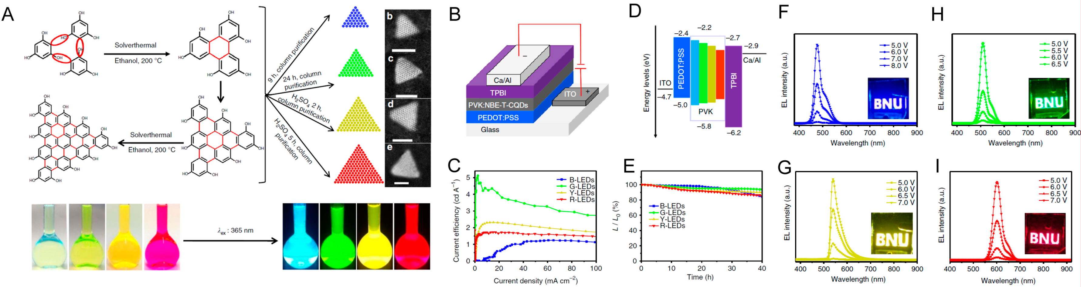
| Phloroglucinol | triangular 1.9 nm | 476 | 1882 | 1.22 | [78] |
| 2.4 nm | 510 | 4762 | 5.11 | ||
| 3 nm | 540 | 2784 | 2.31 | ||
| 3.9 nm | 602 | 2344 | 1.73 | ||
| Citric acid with 2,3-diaminonaphthalene | 2.41 nm | 536 | 2050 | 1.1 | [65] |
| human hair | 2D array of CDs 2–6 nm | 498 | 350 | 0.22 | [79] |
| 700 | 0.2 | ||||
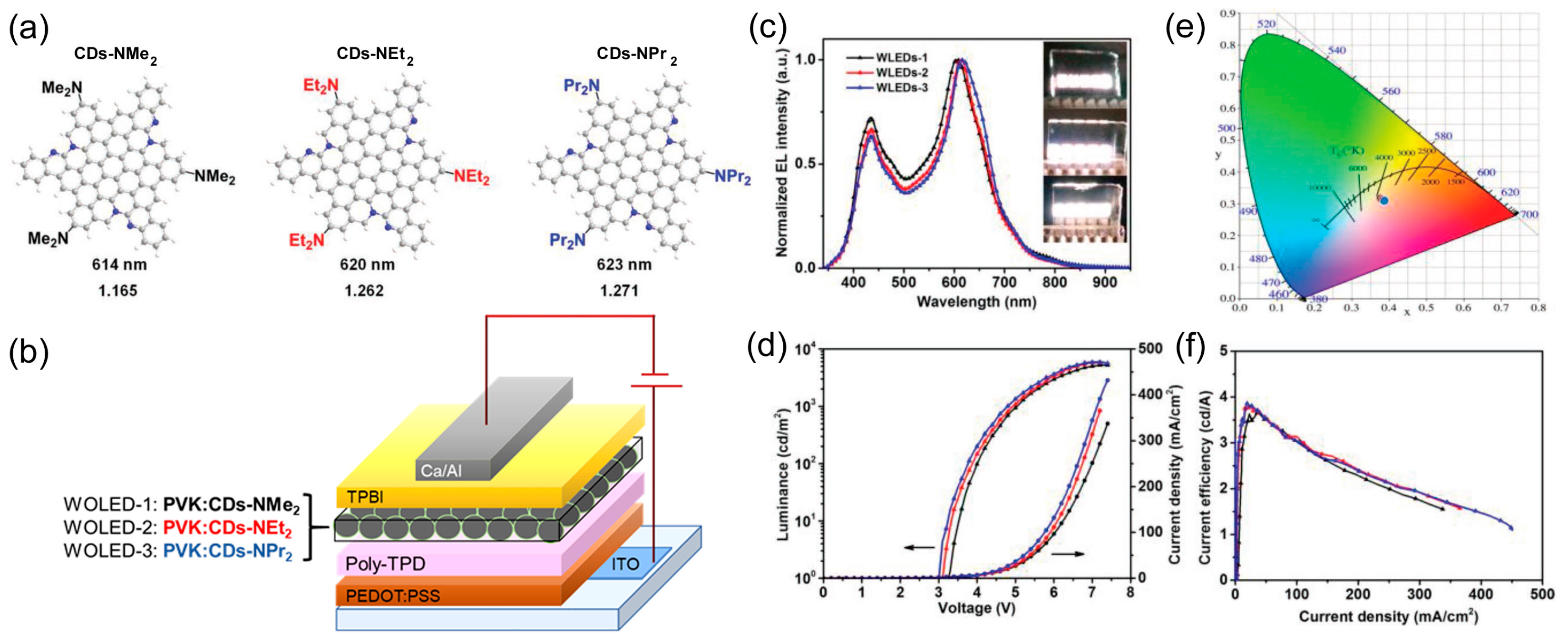
| N,N-dimethyl-, N,N-diethyl-, and N,N-dipropyl-p-phenylenediamine | quasi-spherical 2.2 ± 0.31. 2.3 ± 0.28. 2.3 ± 0.26 nm lattice spacing 0.21 nm | 605/434 612/435 616/435 | 5248–5909 | 3.65 3.85 | [80] |
| anhydrous citric acid and hexadecylamine | spherical_2.0–2.5 nm lattice spacing 0.22 | 558-550 | 339.5–455.2 | - | [73] |
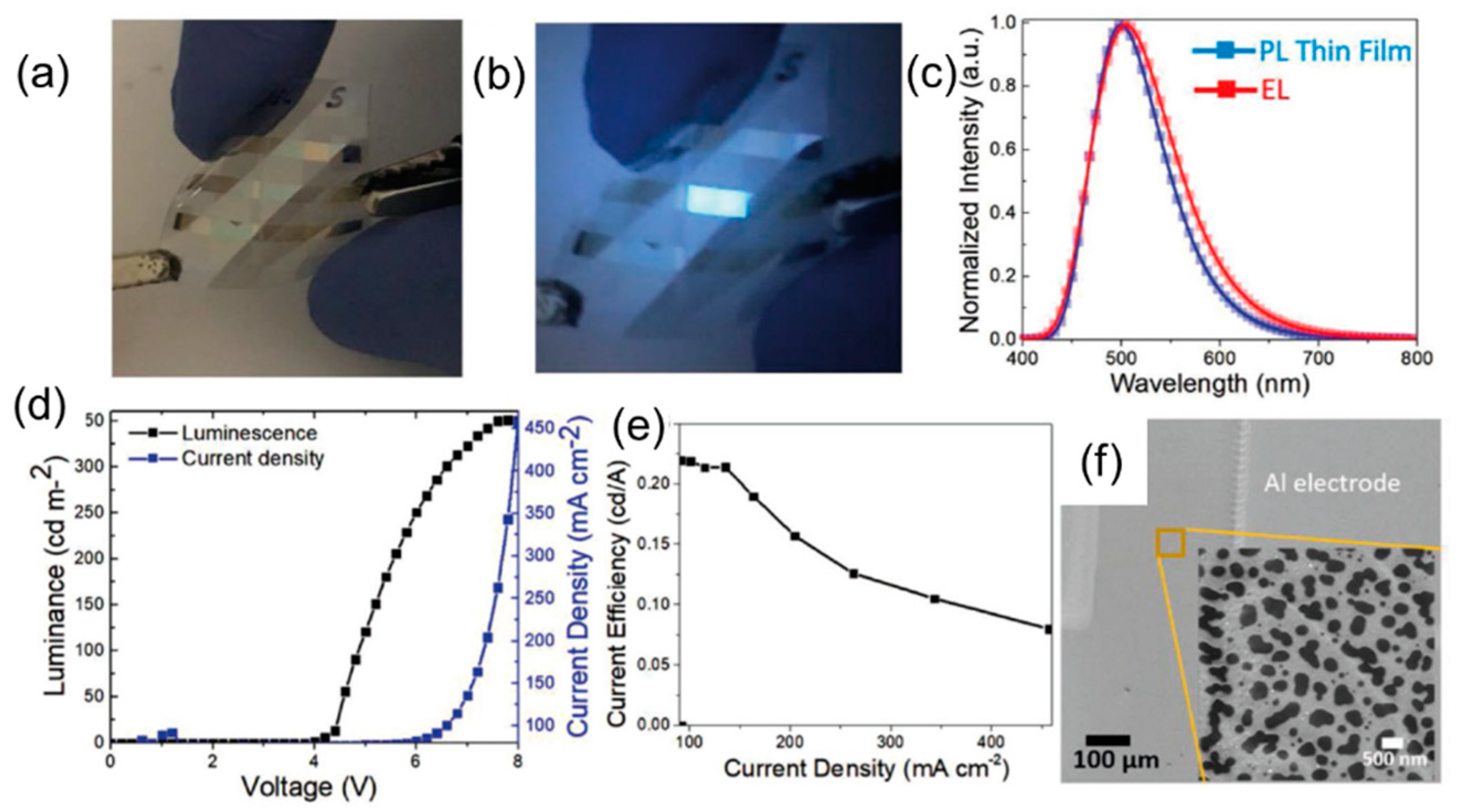
| anhydrous citric acid and hexadecylamine | - | 474 | 569.8 | - | [81] |
| CDs as interlayer | - | - | - | - | - |
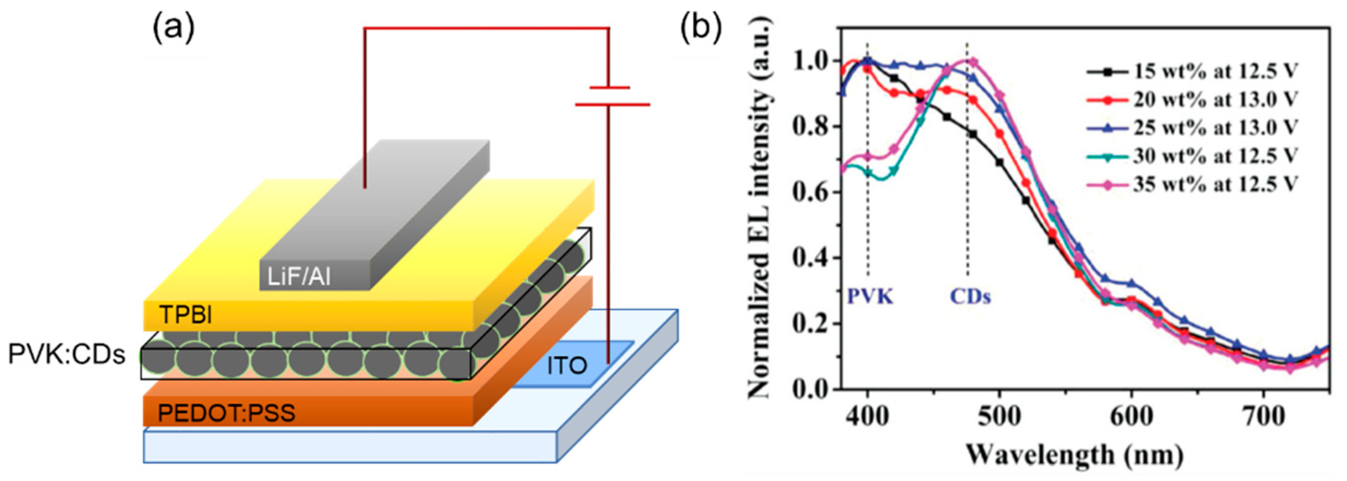
| ethylenediamine and citric acid | - | 532 | 30 730 | 93.8 | [82] |
| banana leaves | 4–6 nm (quasi-spherical) | 486 | - | - | [83] |
| Ethanolamine | - | 622 | 3500 | 0.63 | [84] |
| Hole Transport Materials | Capping Ligand Hole Mobility a | LMAX (cd/m2) | ηc (cd/A) |
|---|---|---|---|
| C-Dots-EDA | 2.41 ± 0.60 | 70 | 2 × 10⁻³ |
| C-Dots-PDA | 1.5 ± 0.47 | 13 | 9 × 10⁻⁴ |
| C-Dots-HDA | 85.4 ± 1.7 | 174 | 8 × 10⁻⁴ |
| C-Dots-Urea | 2.92 ± 0.32 | 146 | 2 × 10⁻³ |
| No HTM (control) | - | 2 | 5 × 10⁻⁴ |
Publisher’s Note: MDPI stays neutral with regard to jurisdictional claims in published maps and institutional affiliations. |
© 2020 by the authors. Licensee MDPI, Basel, Switzerland. This article is an open access article distributed under the terms and conditions of the Creative Commons Attribution (CC BY) license (http://creativecommons.org/licenses/by/4.0/).
Share and Cite
Lagonegro, P.; Giovanella, U.; Pasini, M. Carbon Dots as a Sustainable New Platform for Organic Light Emitting Diode. Coatings 2021, 11, 5. https://doi.org/10.3390/coatings11010005
Lagonegro P, Giovanella U, Pasini M. Carbon Dots as a Sustainable New Platform for Organic Light Emitting Diode. Coatings. 2021; 11(1):5. https://doi.org/10.3390/coatings11010005
Chicago/Turabian StyleLagonegro, Paola, Umberto Giovanella, and Mariacecilia Pasini. 2021. "Carbon Dots as a Sustainable New Platform for Organic Light Emitting Diode" Coatings 11, no. 1: 5. https://doi.org/10.3390/coatings11010005
APA StyleLagonegro, P., Giovanella, U., & Pasini, M. (2021). Carbon Dots as a Sustainable New Platform for Organic Light Emitting Diode. Coatings, 11(1), 5. https://doi.org/10.3390/coatings11010005