Letter

Growth of Si3N4 Thin Films on Si(111) Surface by RF-N2 Plasma Nitriding

1
National Applied Research Laboratories, Taiwan Instrument Research Institute, Hsinchu Taiwan 20. R&D Rd. VI, Hsinchu Science Park, Hsinchu 300092, Taiwan
2
Department of Mechatronic Engineering, National Taiwan Normal University, Taipei Taiwan 162, Section 1, Heping E. Rd., Taipei City 10610, Taiwan
3
National Applied Research Laboratories, Taiwan Semiconductor Research Institute, 26, Prosperity Road I, Hsinchu Science Park, Hsinchu 300091, Taiwan
*
Author to whom correspondence should be addressed.
Coatings 2021, 11(1), 2; https://doi.org/10.3390/coatings11010002
Submission received: 27 October 2020 / Revised: 7 December 2020 / Accepted: 8 December 2020 / Published: 22 December 2020
(This article belongs to the Special Issue Surface Plasma Treatments)

Abstract

:
Ultra-thin Si3N4 films were grown on Si(111) surface by radio frequency (RF)-N2 plasma exposure at 900 °C with 1–1.2 sccm of a flux of atomic nitrogen. We discuss the effect of various conditions such as N2 flow rate, nitriding time and RF power on the optical, chemical, and structural properties of a nitrided Si3N4 layer. The optical properties, surface morphology and chemical composition are investigated by using ellipsometry, atomic force microscopy (AFM), X-ray photoelectron spectroscopy (XPS), and transmission electron microscopy (TEM). Cross-sectional TEM images show that an RF power of 350 W induced some damage to the Si(111) surface. The thickness of nitrided Si3N4 was measured to be about 5–7 nm. XPS results shown that the binding energy of Si 2p3/2 located at 101.9 ± 0.1 eV is attributed to the Si–N bonds in the Si3N4 compound. Smooth Si3N4 ultra-thin films were obtained at a nitridation time close to 1 h with an RF power of 300 W, with a measured refractive index (n) nearly to 1.88 at 632 nm. The increase in refractive index with decreased RF-plasma power and nitrogen flow rate is probably attributed to the change in the stoichiometry of the film and less surface damage.

1. Introduction

Silicon nitride (SixNy, normally Si3N4) is a ceramic material that has drawn widespread attention in studies related to microelectronic applications. It can also be used as a coating layer in high-temperature and corrosive environments [1]. Its high-temperature properties are better than most metals, combining high mechanical strength and creep resistance and good oxidation resistance. In addition, Si3N4 has good thermal shock resistance compared with most ceramic materials, attributed to its low thermal expansion coefficient. There are two well-known structures of silicon nitride: α-Si3N4 and β-Si3N4; both have a hexagonal structure. Among them, α-Si3N4 and β-Si3N4 can be formed under normal pressure, while γ-Si3N4 (cubic spinel lattice) can be formed under a high temperature and pressure [2,3,4]. In addition, it is used as a wide-band-gap semiconductor (e.g., 4.7 eV) [5,6]. Growth of high-quality silicon nitride is very important due to its wide applications in microelectronics such as etch masks [7], and a buffer layer for III-nitride growth [8]. Recently, the growth of group III–Nitride on Si substrate has been very important for the mass production of high electron mobility transistors (HEMTs) due to the low cost, large surface area, and high thermal conductivity of Si substrates. Therefore, crystalline Si3N4 films are used as a buffer layer for III–nitride growth on silicon substrate [9]. Nakada et al. report that the dislocation density in heteroepitaxial GaN layers can also be reduced by using a silicon nitride buffer layer [10], which leads to the prospect of silicon-based integrated optoelectronic circuits (Si-OEICs) with silicon-based devices. Epitaxial growth of Si3N4 film on Si(111) is also theoretically possible because of the good match in lattice parameters between Si(111) and Si3N4(0001). However, the growth of high-quality crystalline Si3N4 is very difficult due to the low self-diffusion coefficient of nitrogen in Si3N4 caused by its density. [11]. On the other hand, Si3N4 films deposited on Si are usually amorphous. However, due to a nearly perfect lattice match, the 2 × 2 unit cell of the Si(111) surface is only ~1.1% larger than the unit cell of β-Si3N4(0001) [12]. Recently, various methods have been used to fabricate Si3N4 films, including thermal chemical vapor deposition (CVD) [13], plasma-enhanced/low-pressure CVD [14], microwave plasma nitriding [15], radio frequency (RF) sputtering [16], and various gas plasma nitridation such as NO [17], N2 [18], N [19], or N [20] ion beam at high substrate temperatures. Although CVD and sputtering have often been used in the growth of Si3N4 thin films, few studies have reported nitrided Si3N4 grown directly on a Si(111) substrate using RF-metal–organic molecular-beam epitaxy (MOMBE).
Nitridation occurs when a silicon substrate is exposed to gases such as NH3 [21], NO [17], and N2H4 [22], or to N atoms and ions [1]. For nitridation of Si by plasma-assisted molecular-beam epitaxy (MBE)-related systems which can lower the nitridation temperature below NH3-MBE (such as 700–900 °C for RF-MBE [23], 800–1100 °C for NH3-MBE [24]), the control of nitrogen flux is an important issue because the nitridation area and rate are affected by the amount of nitrogen atom flux [25].
Previous work on nitriding Si for the formation of Si3N4 has been performed with thermal and radio frequency plasma processing using NH3, N2, and H2 [26,27,28]. Zhai et al. reported that a coherent Si3N4(0001)/Si(111) interface can be formed using a thermal nitridation process, where the Si substrate is exposed to nitrogen-containing gases such as NH3 at high substrate temperatures [29]. Due to its inertness, growth of Si3N4 by nitriding to N2 requires relatively high pressures, and it is highly sensitive to contamination in the supplied gas. In previous reports, Ermolieff et al. and Bolmont et al. repored that the nitriding process of Si(111) [30] and Si(100) [31] used a flux in atomic N at low temperature [32].
Optoelectronic devices of III–nitride on Si substrate are very attractive due to the cost-effective device fabrication on the platform of Si-based integrated circuits [33]. However, the difference in the thermal expansion coefficients and lattice mismatch between nitride and Si can lead to cracking of III–N epitaxial layers [34].
Silicon-based materials have the advantages of compatibility with current silicon technology and lower cost compared to compound materials. On the other hand, the growth mechanism of silicon nitride films on silicon and their morphology, including the surface atomic structures, are important to these applications. Our current knowledge of these fundamental properties, however, is quite limited. Therefore, in the present work, we explore the effect of RF-plasma nitriding on crystalline Si3N4 formation on nitrided Si(111) substrate. The substrate was nitrided at 900 °C for 60 min at various nitridation conditions. The effects of nitridation conditions on the structural and optical properties and surface morphology of the Si3N4 films were then investigated. The effectiveness of this method is evaluated using ellipsometry, atomic force microscopy (AFM), transmission electron microscopy (TEM), and XPS.

2. Materials and Methods

Crystalline Si3N4 ultra-thin films were grown on a Si(111) surface using RF-N2 plasma exposure at various RF powers and N2 flow rates and a fixed nitridation time. The nitridation process was performed in the growth chamber of self-designed UHV-RF-MBE (home-made). The active nitrogen (N + N*) radicals were generated by a 13.56 MHz RF-plasma source with a high pure N2 (99.9999%) gas. The growth chamber was vacuumed by a turbo molecular pump to reach a base pressure of 1 × 10⁻⁹ Torr. The substrate were 20 × 20 mm2 slabs cut from Si(111) wafer. The silicon wafers were cleaned by Radio Corporation of America (RCA) clean and then dipped in Buffered Oxide Etch (BOE) solvent for 10 min to remove the native oxide of silicon surface. Prior to the nitridation process, the cleaned silicon substrate was placed in an ultra-high-vacuum chamber (base pressure ~1 × 10⁻⁹ Torr) and thermally annealed at 900 °C for more than 120 min to remove the remaining thin native oxide. After this, the substrate was exposed to a flux of atomic nitrogen generated by a RF-plasma source for 60 min with RF ~300, 350 W and N2 ~1, 1.2 sccm. During the silicon nitrided growth, the N2 gas flow and the reactor pressure were maintained at a constant. The work pressure corresponded to 1 × 10⁻⁵ Torr and 1.2 × 10⁻⁵ Torr with N2 flow rate at 1 and 1.2 sccm, resistively. The detailed experimental conditions of the nitrided Si3N4 layer were listed in Table 1. Various properties of nitrided Si3N4 ultra-thin films were measured by ellipsometry (SENTECH Instruments GmbH, Berlin, Germany), AFM, and TEM analysis. The chemical evolution of the nitridation layer has been studied by x-ray photoelectron spectroscopy (XPS; VG ESCA/XPS Theta Probe; Thermo Fisher Scientific Inc., Waltham, MA, USA). The XPS experiments were performed in a VG ESCA Scientific Theta Probe using Al Kα ( = 1486.6 eV) radiation to characterize the bonding characteristics of elements in the films. The surface morphologies and cross-section microstructure of the films were analyzed using an atomic force microscope (AFM, Dimension 3100 SPM, Digital Instruments, Tonawanda, NY, USA) with the tapping mode and a transmission electron microscope (TEM, Philips Tecnai 20 Amsterdam, The Netherlands).

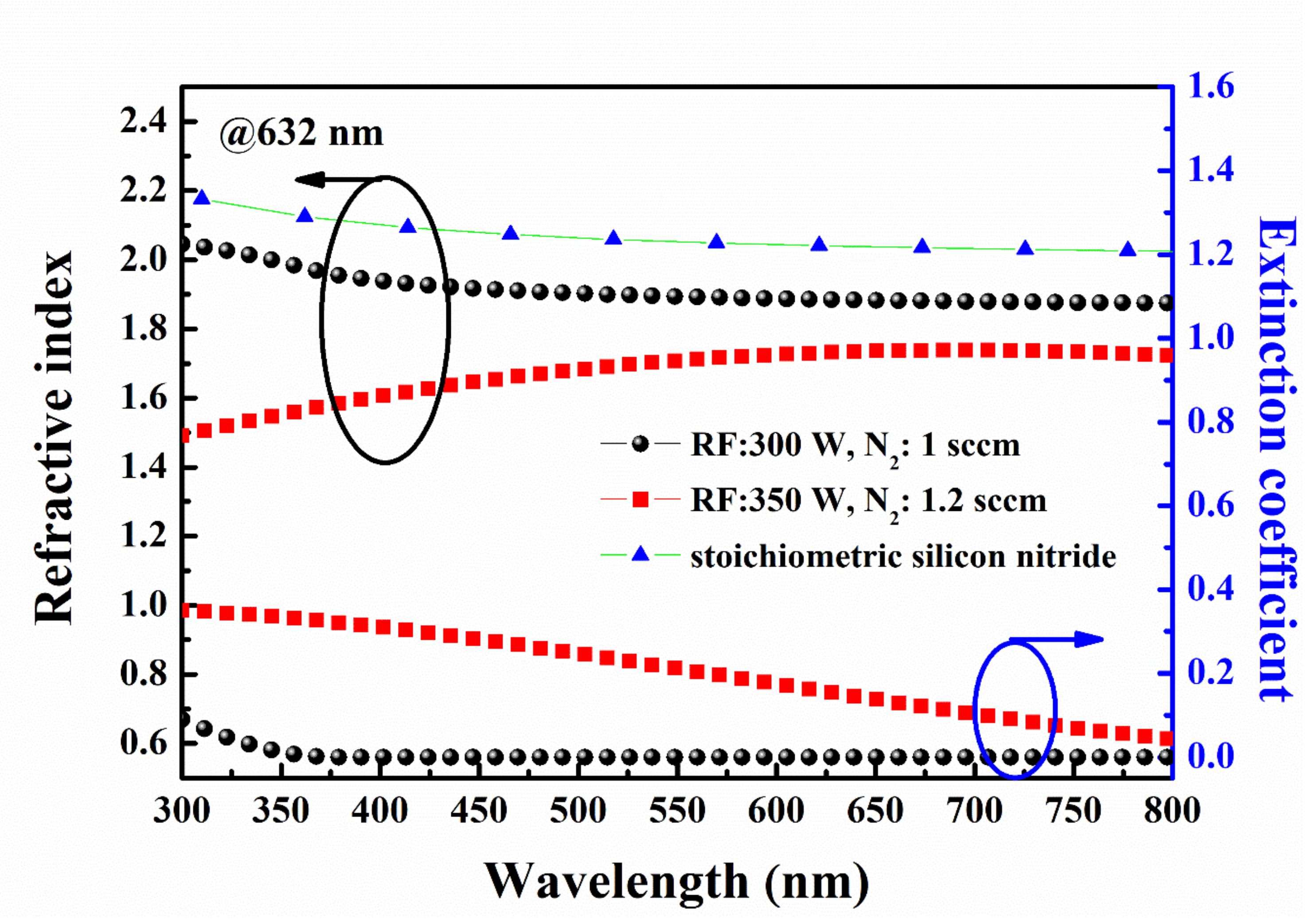
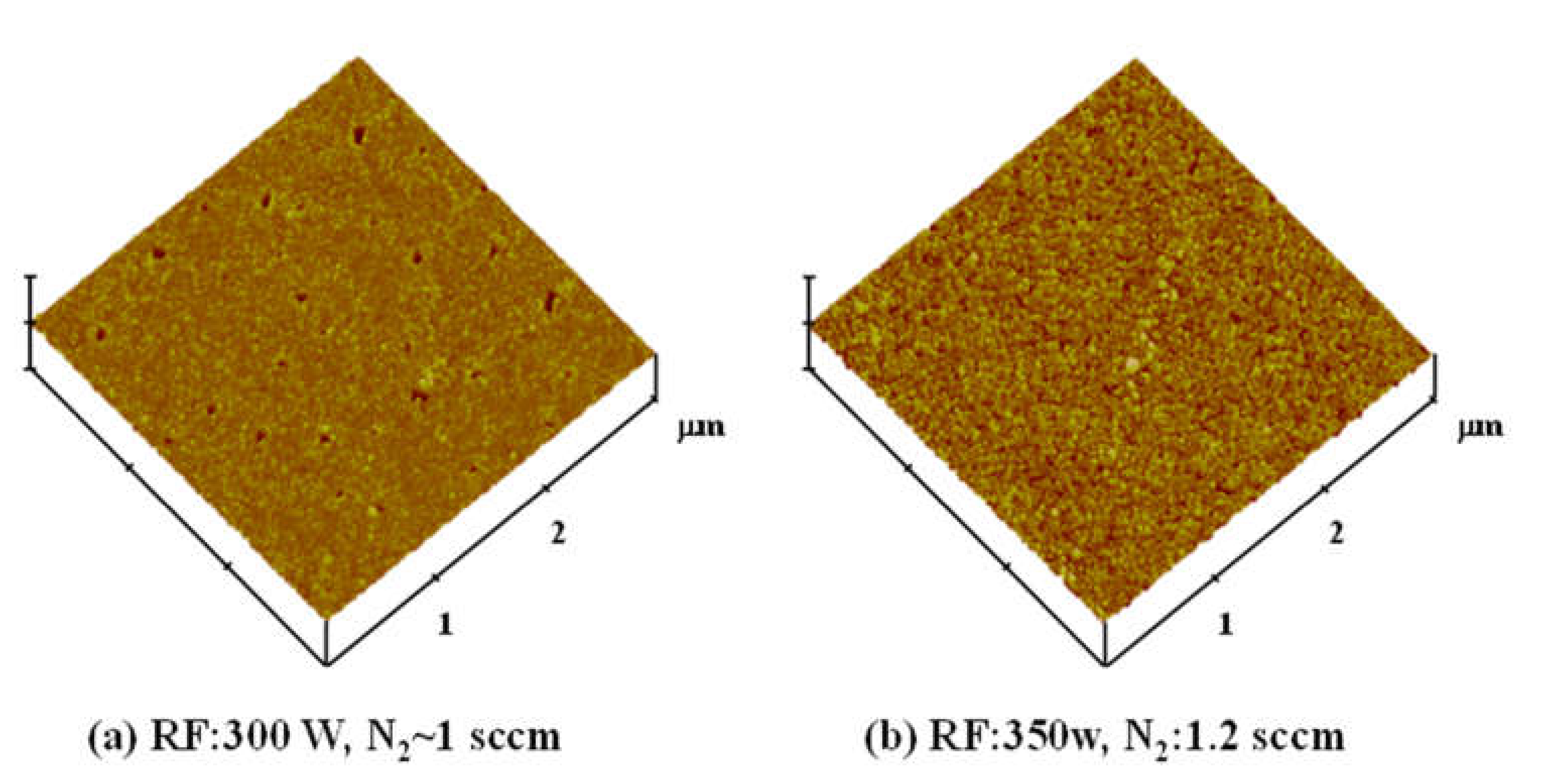
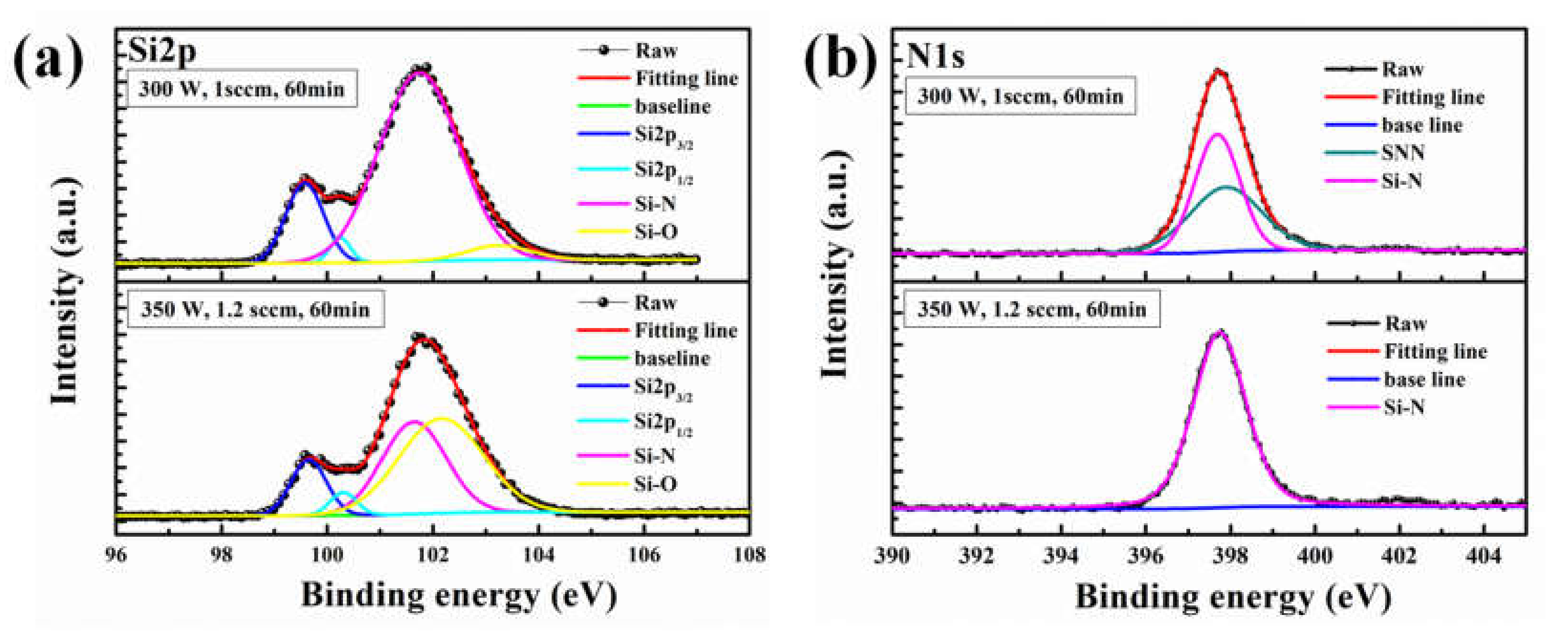
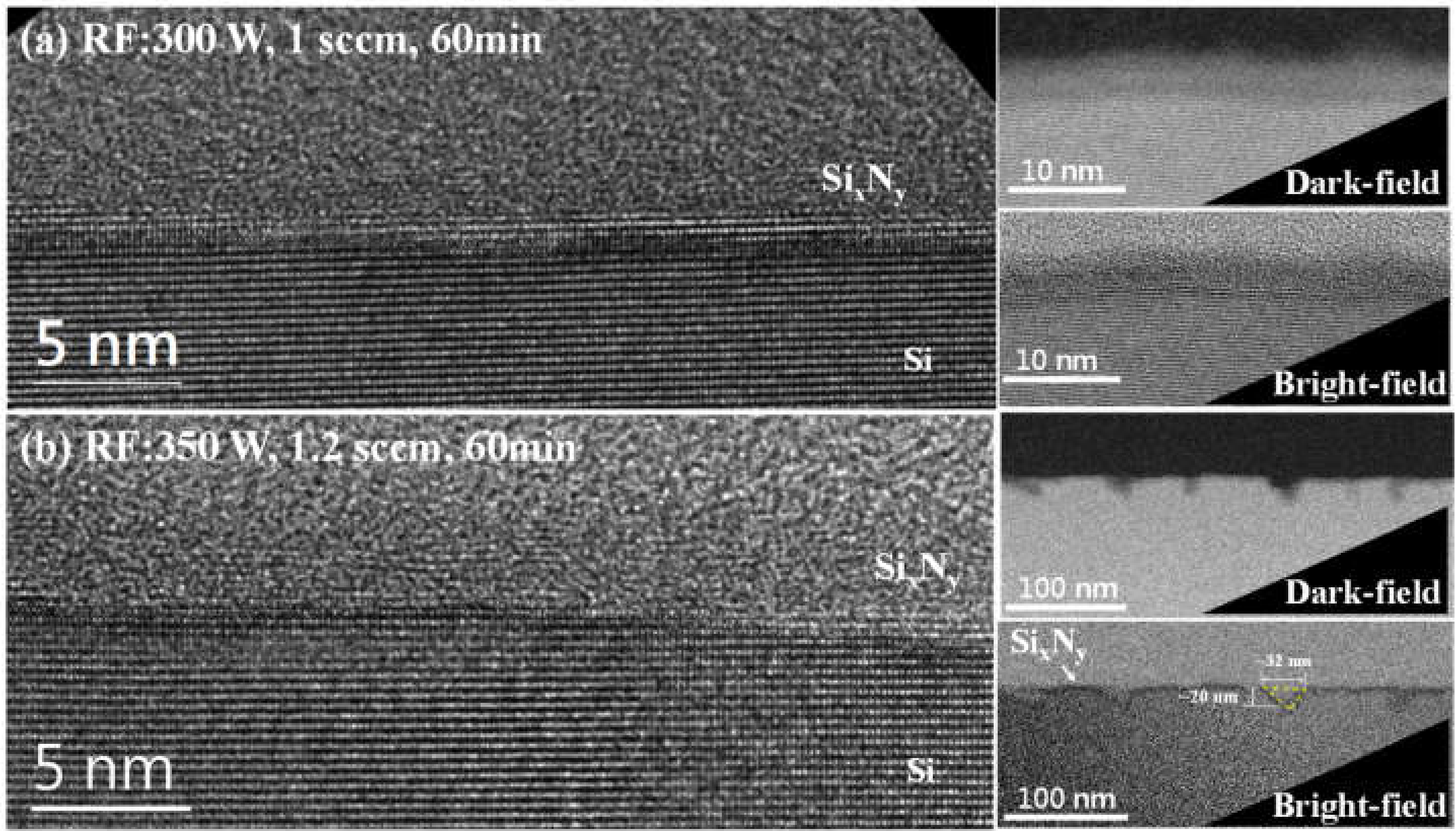
3. Results and Discussion

The thickness and refractive index of all the nitrided Si3N4 layers were characterized by spectroscopic ellipsometry. The refractive index of Si3N4 layer is fitted by the Tauc-Lorentz models at wavelengths ranging from 300 to 800 nm, using an angle of incidence of 75° and an illumination spot diameter of 1.0 mm. The measured dispersion of the refractive index and extinction coefficient of silicon nitride at 632 nm are shown in Figure 1. The data for stoichiometric silicon nitride [35] are also shown for comparison. In the visible wavelength range, silicon nitride film thickness and refractive index were determined by ellipsometry measurements of 5 (±0.1) nm and 1.88 (±0.10) for sample A, and 7 (±0.1) nm and 1.73 (±0.10) for sample B, respectively. The surface roughness of the samples was obtained using the AFM, and the value of surface roughness is 15%–20% of the thickness. Therefore, the surface roughness may impact thickness analysis in fitting result. The refractive-index values are smaller than that the corresponding average values for stoichiometric silicon nitride film (refractive index ~2.02 at 300 K) [36]. The value of the fitted film thickness closely matches the data obtained from the cross-section TEM image. For sample A (RF: 300 W with N2: 1 sccm), it can be seen that the silicon nitride is characterized by slightly weaker variation with wavelength and smaller refractive index. This is due to the fact that the surface morphology shows some pits on the SixNy thin film surface, possibly attributable to plasma damage. For RF power at 300 W with N2 ~1 sccm, the value of the refractive index at 632 nm of nitrided SixNy is ~7% smaller than that of stoichiometric silicon nitride. The result indicated that the decrease may be caused by the physical and chemical structural modifications induced in the SixNy by the nitridation process. However, the measured shrinkage was small, which clearly indicates that the physical modifications (such as pits) within the structure of the nitrided SixNy are the main cause for the refractive-index variation. In addition, for RF power at 350 W with N2 ~1.2 sccm, the SixNy thin film shows large variation, probably due to nonstoichiometric Si–N–O compounds (n = 1.457-1.909 at 632.8 nm) and/or high-density pits. In addition, extinction coefficients of sample A are smaller than 1 × 10⁻⁴. However, sample B shows that the extinction coefficients were nearly 0.15, which is probably due to nonstoichiometric Si–N–O compounds.
Figure 2 shows AFM images of the surfaces of two samples. The root mean square (RMS) surface roughness values were measured from 3 × 3 μm2 AFM scans. The RMS roughness of nitrided SixNy was found to increase with increasing RF power and nitrogen flow from 0.891 nm for RF: 300 W with 1 sccm of N2 flow rate to 1.089 nm for RF: 350 W with 1.2 sccm of N2 flow rate. The AFM image of sample A (RF: 300 W with N2: 1 sccm) is shown in Figure 2a. The image shows irregular shape surface pits with diameters in the range 20–30 nm, which suggests that the plasma nitriding process induced damage to the surface of the samples. AFM images of the surface of sample B (RF: 350 W with N2: 1.2 sccm) are also shown in Figure 2b. The image exhibits rough surface morphology with the pits of high density. Surface pit density was measured by AFM image analysis with ImageJ software. Its analysis resulted in a count of 45 and 835 pits, leading to a density of 3 × 1010 cm−2 and 7.6 × 1012 cm−2 for sample A and sample B, respectively.
Two elemental species, Si, and N, were identified in the films by their corresponding signals observed in the XPS spectra. Figure 3 shows two samples of the Si 2p and N 1s spectra for the Si–N films prepared at various conditions. A Gaussian–Lorentzian sum function was used in the fitting, and the results are shown as red solid lines. The spectrum shows two main peaks at 99.5 and 101.78 eV. In order to investigate the Si-related peak in more detail, measurement and fitting were analyzed in a high-resolution spectrum. The peak in Si 2p and N 1s exhibit a slightly asymmetric shape, suggesting that they have several bonds other than Si–N in the SixNy layer. The asymmetric peaks were fitted by using a linear combination of Gaussian and Lorentzian line shapes commonly referred to as a pseudo-Voigt function [37]. The peak can be deconvoluted to three components (Figure 3a), which correspond to silicon nitride, silicon oxide, and silicon [38]. XPS spectra results indicated that the binding energy of Si 2p3/2 and Si 2p1/2 spin-orbit doublets located at around at 99.48 and 100.03 eV ± 0.1 eV and equal to 0.63 eV are characteristic of the Si–Si bonds. For the sample A (RF: 300 W with N2: 1 sccm), the spectra corresponding to the surface of Si show a strong peak at 101.7 eV, which is assigned to the binding energy of Si–N in the nitride compounds. Additionally, the weak broad peak centered at 103.18 ± 0.1 eV was attributed to Si–O–C and/or the silicon oxide band [39]. In previous reports, the N 1s peak for bulk Si3N4 was observed at 397.88 eV where the second nearest neighbor (SNN) was nitrogen [40], and N [Si(Si)3]3 was observed at 397.5 ± 0.2 eV with the Si atoms being SNNs to nitrogen [41]. On the other hand, thick SixNy (~7 nm) obtained for 60 min of nitridation with 350 W of RF power suggests that the diffusion length for the nitridant species across the nitrided Si and/or an amorphous SiO2 region was greater than the SixNy obtained. For the binding energies of Si and N in sample B, as shown in Figure 3a,b, the nitrided film can be clearly identified as SiNO. These results indicate that a higher process temperature offers more reactions between N radicals of the plasma and the Si atoms on the surface. The result is similar to that reported by Wu et al. [42].
The microstructures of the nitrided SixNy were characterized by TEM. The cross-sectional TEM (XTEM) specimens were prepared from the grown layers. Figure 4 shows bright-field TEM images of nitrided SixNy grown on the Si(111) substrate under various conditions. As estimated from cross-sectional TEM images, the thickness of the all nitrided SixNy thin films were approximately ~5 nm for sample A (RF: 300 W with N2: 1 sccm), and ~7 nm for sample B (RF: 350 W with N2: 1.2 sccm), respectively. The results are in agreement with the ellipsometry measured values. For sample A, the TEM images showed that the nitrided SixNy films were grown continuously by plasma nitriding. In addition, when RF power was increased to 350 W, the surface morphology exhibited rough features, in agreement with the AFM results. Further, bright- and dark-field images revealed that non-continuous V-like pits formed in both film and substrate regions, indicating that the result is probably caused by plasma damage to the nonstoichiometric silicon nitride layer [43], as shown in Figure 4b. The typical depth and width of the V-like pits was measured to be approximately 20 and 24 nm in average, respectively. Nevertheless, the structural and morphological characterizations imply that the substrate nitriding with a lower RF power and N2 flow rate is always beneficial for the crystal quality of the epitaxial Si3N4 layer on silicon.

4. Conclusions

We fabricated crystalline Si–N ultra-thin layer nitrided Si(111) substrates via RF-N2 plasma and studied the effect of nitridation conditions on the surface, structural, morphological, and compositional properties of the Si–N ultra-thin layer. RF-plasma exposure of Si(111) substrate to a flux of atomic N is suitable for growing ultra-thin layers of silicon nitride. XPS analysis indicated at thsilicon nitride was formed in the nitrided Si and/or an amorphous SiO2. In order to investigate this in more detail, nitriding of the Si 2p peak from sample B exhibits a slightly larger broadening peak than that sample A, suggesting that there may be two different bonding in the nitrided film, where the major one is Si–N (101.7 eV) and the others are minor Si–O–C bonds (103.18 eV). AFM images show that surface of the nitrided Si(111) substrate was rough, likely as a result of damage from the RF-plasma beam. TEM results show that the thickness of silicon nitride formed via nitridation of the Si(111) substrate can be tuned from the ultra-thin (~5 nm) to a thin regime (~7 nm) by varying the nitrogen flow and RF power from 1 to 1.2 sccm and 300 to 350 W, respectively. The XTEM image shows that silicon nitride was nano-crystalline on the surface of Si(111) due to plasma nitriding. These results indicate that the nitrided Si(111) substrate is essential for engineering the growth of nitride on Si wafers.

Author Contributions

W.-C.C. carried out most of the experimental work, including the preparation and characterization of Si3N4 layer and the drafting of the manuscript. T.-Y.Y. carried out the high-resolution XPS measurements. S.C., J.S., Y.-W.L., H.-P.C. and C.-P.C. supported the analysis of the Si–N samples. All authors have read and agreed to the published version of the manuscript.

Funding

This research was funded by the Ministry of Science and Technology, grant number MOST 109-2221-E-492-013 and MOST 108-2221-E-492-017.

Conflicts of Interest

The authors declare no conflict of interest.

References

  1. Ma, T.P. Making silicon nitride film a viable gate dielectric. IEEE Trans. Electron Devices 1998, 45, 680–690. [Google Scholar] [CrossRef]
  2. Riley, F.L. Silicon nitride and related materials. J. Am. Ceram. Soc. 2000, 83, 245–265. [Google Scholar] [CrossRef]
  3. Murakawa, S.; Ishizuka, S.; Nakanishi, T.; Suwa, T.; Teramoto, A.; Sugawa, S.; Hattori, T.; Ohmi, T. Depth profile of nitrogen atoms in silicon oxynitride films formed by low-electron-temperature microwave plasma nitridation. Jpn. J. Appl. Phys. 2010, 49, 49. [Google Scholar] [CrossRef]
  4. Higuchi, M.; Aratani, T.; Hamada, T.; Teramoto, A.; Hattori, T.; Sugawa, S.; Ohmi, T.; Shinagawa, S.; Nohira, H.; Ikenaga, E.; et al. Electric characteristics of Si3N4 films formed by directly radical nitridation on Si (110) and Si (100) surfaces. Solid State Devices Mater. 2006. [Google Scholar] [CrossRef] [Green Version]
  5. Unal, O.; Petrovic, J.J.; Mitchell, T.E. CVD Si3N4 on single crystal SiC: Part I, Characterization and orientation relationships at the interface. J. Mater. Res. 1992, 7, 136–147. [Google Scholar] [CrossRef]
  6. Kim, J.W.; Yeom, H.W. Surface and interface structures of epitaxial silicon nitride on Si. Phys. Rev. B 2003, 67, 035304. [Google Scholar] [CrossRef]
  7. Hwang, W.S.; Cho, B.J.; Chan, D.S.H. Effects of SiO2/Si3N4 hard masks on etching properties of metal gates. J. Vac. Sci. Technol. B 2006, 24, 2689–2694. [Google Scholar] [CrossRef]
  8. Kumar, M.; Rajpalke, M.K.; Roul, B.; Bhat, T.N.; Sinha, N.; Kalghatgi, A.T.; Krupanidhi, S.B. The impact of ultra thin silicon nitride buffer layer on GaN growth on Si (1 1 1) by RF-MBE. Appl. Surf. Sci. 2011, 257, 2107–2110. [Google Scholar] [CrossRef]
  9. Kumar, M.; Roul, B.; Bhat, T.N.; Rajpalke, M.K.; Misra, P.; Kukreja, L.M.; Sinha, N.; Kalghatgi, A.T.; Krupanidhi, S.B. Improved growth of GaN layers on ultra thin silicon nitride/Si (111) by RFMBE. Mater. Res. Bull. 2010, 45, 1581–1585. [Google Scholar] [CrossRef]
  10. Nakada, Y.; Aksenov, I.; Okumura, H. GaN heteroepitaxial growth on silicon nitride buffer layers formed on Si(111) surfaces by plasma-assisted molecular beam epitaxy. Appl. Phys. Lett. 1998, 73, 827–829. [Google Scholar] [CrossRef]
  11. Kijima, K.; Shirasaki, S. Nitrogen self-diffusion in silicon nitride. J. Chem. Phys. 1976, 65, 2668–2671. [Google Scholar] [CrossRef]
  12. Xu, Y.N.; Ching, W.Y. Electronic structure and optical properties of α and β phases of silicon nitride, silicon oxynitride, and with comparison to silicon dioxide. Phys. Rev. B 1995, 51, 17379. [Google Scholar] [CrossRef] [PubMed]
  13. Pandey, R.K.; Patil, L.S.; Bange, J.P.; Gautam, D.K. Growth and characterization of silicon nitride films for optoelectronics applications. Opt. Mater. 2004, 27, 139–146. [Google Scholar] [CrossRef]
  14. Yang, C.; Pham, J. Characteristic study of silicon nitride films deposited by LPCVD and PECVD. Silicon 2018, 10, 2561. [Google Scholar] [CrossRef]
  15. Yu, C.H.; Chiu, K.A.; Do, T.H.; Chang, L. Oriented Si3N4 crystallites formed by plasma nitriding of SiO2/Si (111) substrate. Surf. Coat. Technol. 2020, 395, 125877. [Google Scholar] [CrossRef]
  16. Signore, M.A.; Sytchkova, A.; Dimaio, D.; Cappello, A.; Rizzo, A. Deposition of silicon nitride thin films by RF magnetron sputtering: A material and growth process study. Opt. Mater. 2012, 34, 632–638. [Google Scholar] [CrossRef]
  17. Röttger, B.; Kliese, R.; Neddermeyer, H. Adsorption and reaction of NO on Si(111) studied by scanning tunneling microscopy. J. Vac. Sci. Technol. B 1996, 14, 1051. [Google Scholar] [CrossRef]
  18. Morita, Y.; Tokumoto, H. Origin of the 8/3 × 8/3 superstructure in STM images of the Si(111)-8×8:N surface. Surf. Sci. 1999, 443, L1037–L1042. [Google Scholar] [CrossRef]
  19. Schrott, A.G.; Fain, S.C., Jr. Nitridation of Si(111) by nitrogen atoms. Surf. Sci. 1982, 123, 204–222. [Google Scholar] [CrossRef]
  20. Ha, J.S.; Park, K.-H.; Yun, W.S.; Lee, E.-H.; Park, S.-J. Interaction of low-energy nitrogen ions with an Si(111)-7×7 surface: STM and LEED investigations. Appl. Phys. A 1998, 66, S495–S499. [Google Scholar] [CrossRef]
  21. Avouris, P.H.; Wolkow, R. Atom-resolved surface chemistry studied by scanning tunneling microscopy and spectroscopy. Phys. Rev. B 1989, 39, 5091–5100. [Google Scholar] [CrossRef]
  22. Tindall, C.; Li, L.; Takaoka, O.; Hasegawa, Y.; Sakurai, T. Scanning tunneling microscopy of N2H4 on silicon surfaces. Surf. Sci. 1997, 380, 481–488. [Google Scholar] [CrossRef]
  23. Yamabe, N.; Yamamoto, Y.; Ohachi, T. Epitaxial growth of β-Si3N4 by the nitridation of Si with adsorbed N atoms for interface reaction epitaxy of double buffer AlN(0001)/ β-Si3N4/Si(111). Phys. Status Solidi C 2011, 8, 1552–1555. [Google Scholar] [CrossRef]
  24. Hayafuji, Y.; Kajiwara, K. Nitridation of silicon and oxidized-silicon. J. Electrochem. Soc. 1982, 129, 2102–2108. [Google Scholar] [CrossRef]
  25. Ohachi, T.; Yamabe, N.; Shimomura, H.; Shimamura, T.; Ariyada, O.; Wada, M. Measurement of nitrogen atomic flux for RF-MBE growth of GaN and AlN on Si substrates. J. Cryst. Growth 2009, 311, 2987–2991. [Google Scholar] [CrossRef]
  26. Unal, O.; Mitchell, T.E. CVD Si3N4 on Single Crystal SiC: Part II. High resolution electron microscopy and atomic models of the interface. J. Mater. Res. 1992, 7, 1445–1454. [Google Scholar] [CrossRef]
  27. Malvost, H.; Michelt, H.; Ricardt, A. Correlations between active species density and iron nitride layer growth in Ar-N2-H2 microwave post-discharges. J. Phys. D Appl. Phys. 1994, 27, 1328–1332. [Google Scholar] [CrossRef]
  28. Tatarova, E.; Dias, F.M.; Gordiets, B.; Ferreira, C.M. Molecular dissociation in N2-H2 microwave discharges. Plasma Sources Sci. Technol. 2005, 14, 19–31. [Google Scholar] [CrossRef]
  29. Zhai, G.; Yang, J.; Cue, N.; Wang, X.-S. Surface structures of silicon nitride thin films on Si(111). Thin Solid Films 2000, 366, 121–128. [Google Scholar] [CrossRef]
  30. Ermolieff, A.; Bernard, P.; Marthon, S.; Camargo da Costa, J.J. Nitridation of Si(100) made by radio frequency plasma as studied by in situ angular resolved x-ray photoelectron spectroscopy. Appl. Phys. 1986, 60, 3162–3166. [Google Scholar] [CrossRef]
  31. Bolmont, D.; Bischoff, J.L.; Lutz, F.; Kubler, L. Use of an electron cyclotron resonance plasma source for Si(001) 2 × 1 surface nitridation by N2: An X-ray photoemission study. Surf. Sci. 1992, 269, 924–928. [Google Scholar] [CrossRef]
  32. Falta, J.; Schmidt, T.H.; Gangopadhyay, S.; Clausen, T.; Brunke, O.; Flege, J.I.; Heun, S.; Bernstorff, S.; Gregoratti, L.; Kiskinova, M. Ultra-thin high-quality silicon nitride films on Si. Europhys. Lett. 2011, 111, 94. [Google Scholar] [CrossRef]
  33. Zhang, B.; Liu, Y. A review of GaN-based optoelectronic devices on silicon substrate. Chin. Sci. Bull. 2014, 59, 1251–1275. [Google Scholar] [CrossRef]
  34. Dadgar, A.; Bläsing, J.; Diez, A.; Alam, A.; Heuken, M.; Krost, A. Metalorganic chemical vapor phase epitaxy of crack-free GaN on Si (111) exceeding 1 µm in thickness. Jpn. J. Appl. Phys. 2000, 39, L1183–L1185. [Google Scholar] [CrossRef]
  35. Luke, K.; Okawachi, Y.; Lamont, M.R.E.; Gaeta, A.L.; Lipson, M. Broadband mid-infrared frequency comb generation in a Si3N4 microresonator. Opt. Lett. 2015, 40, 4823–4826. [Google Scholar] [CrossRef]
  36. Palik, E. Handbook of Optical Constants of Solids; Academic Press: Orlando, FL, USA, 1985; p. 999. [Google Scholar]
  37. Wertheim, G.K.; Butler, M.A.; West, K.W.; Buchanan, D.N.E. Determination of the Gaussian and Lorentzian content of experimental line shapes. Rev. Sci. Instrum. 1974, 45, 1369–1371. [Google Scholar] [CrossRef]
  38. Caballero, D.; Martinez, E.; Bausells, J.; Errachid, A.; Samitier, J. Impedimetric immunosensor for human serum albumin detection on a direct aldehyde-functionalized silicon nitride surface. Anal. Chim. Acta 2012, 720, 43–48. [Google Scholar] [CrossRef]
  39. Li, N.; Hu, P.; Zhang, X.; Liu, Y.; Han, W. Effects of oxygen partial pressure and atomic oxygen on the microstructure of oxide scale of ZrB2–SiC composites at 1500 °C. Corros. Sci. 2013, 73, 44–53. [Google Scholar] [CrossRef]
  40. Kim, J.W.; Yeom, H.W.; Chung, Y.D.; Jeong, K.; Whang, C.N.; Lee, M.K.; Shin, H.J. Chemical configuration of nitrogen in ultrathin Si oxynitride on Si(100). Phys. Rev. B 2002, 66, 035312. [Google Scholar] [CrossRef]
  41. Li, H.-F.; Dimitrijev, S.; Sweatman, D.; Harrison, H.B.; Tanner, P.; Feil, B. Investigation of nitric oxide and Ar annealed SiO2/SiC interfaces by x-ray photoelectron spectroscopy. J. Appl. Phys. 1999, 86, 4316–4321. [Google Scholar] [CrossRef]
  42. Wu, C.; King, C.; Lee, M.; Chen, C. Growth Kinetics of Silicon Thermal Nitridation. J. Electrochem. Soc. 1982, 129, 1559–1563. [Google Scholar] [CrossRef]
  43. Wu, C.-L.; Chen, W.-S.; Su, Y. N2-plasma nitridation on Si(111): Its effect on crystalline silicon nitride growth. Surf. Sci. 2012, 606, L51–L54. [Google Scholar] [CrossRef]
Figure 1. Ellipsometer spectra of SixNy ultra-thin films. For a nitridation time of 60 min, the refractive index (n) of SixNy film is close to 1.88 at 632 nm with RF: 300 W and N2: ~1 sccm.
Coatings 11 00002 g001
Figure 2. (a) Surface morphologies, refractive index, and extinction coefficient of nitrided SixNy grown on Si(111) surface for 60 min with (a) RF: 300 W, N2: ~1 sccm, and (b) RF: 350 W, N2: ~1.2 sccm.
Coatings 11 00002 g002
Figure 3. (a) Si 2p spectra and (b) N 1s spectra of binding energy of nitrided SixNy grown on Si(111) surface for 60 min with RF: 300 W, N2: ~1 sccm, and RF: 350 W, N2: ~1.2 sccm.
Coatings 11 00002 g003
Figure 4. Bright field XTEM images of nitrided SixNy/Si(111) surface for 60 min with (a) RF: 300 W, N2: ~1 sccm, and (b) RF: 350 W, N2: ~1.2 sccm.
Coatings 11 00002 g004
Table 1. Experimental parameters for nitrided Si3N4 layer.
Sample NameSample ASample B
RF power300 W350 W
N2 flow rate1 sccm1.2 sccm
Nitridation time60 min60 min
Publisher’s Note: MDPI stays neutral with regard to jurisdictional claims in published maps and institutional affiliations.

