Zirconium-Aluminum-Oxide Dielectric Layer with High Dielectric and Relatively Low Leakage Prepared by Spin-Coating and the Application in Thin-Film Transistor


 , and
, and 
Abstract
1. Introduction
2. Experimental Detail
2.1. Precursor Solution Synthesis
2.2. Film Fabrication and Characterization
2.3. Metal-Insulator-Metal Device Fabrication and Characterization
2.4. Thin-Film Transistor Applications and Characterization
3. Result and Discussion
4. Conclusions
Author Contributions
Funding
Conflicts of Interest
References
- Yabuta, H.; Masafumi, S.; Katsumi, A.; Toshiaki, A.; Tohru, D.; Hideya, K. High-mobility thin-film transistor with amorphous InGaZnO4 channel fabricated by room temperature rf-magnetron sputtering. Appl. Phys. Lett. 2006, 89, 112123. [Google Scholar] [CrossRef]
- Powell, M.J. The physics of amorphous-silicon thin-film transistors. IEEE Trans. Electron Devices 1989, 36, 2753–2763. [Google Scholar] [CrossRef]
- Park, J.S.; Maeng, W.-J.; Kim, H.-S.; Park, J.-S. Review of recent developments in amorphous oxide semiconductor thin-film transistor devices. Thin Solid Films 2012, 520, 1679–1693. [Google Scholar] [CrossRef]
- Lin, C.-C. Effects of screen luminance combination and text color on visual performance with TFT-LCD. Int. J. Ind. Ergon. 2005, 35, 229–235. [Google Scholar] [CrossRef]
- Katayama, M. Tft-lcd technology. Thin Solid Films 1999, 341, 140–147. [Google Scholar] [CrossRef]
- Gao, Y.; Xu, Y.; Lu, J.; Zhang, J.; Li, X. Solution processable amorphous hafnium silicate dielectrics and their application in oxide thin film transistors. J. Mater. Chem. C 2015, 3, 11497–11504. [Google Scholar] [CrossRef]
- Kwon, J.-Y.; Jung, J.S.; Son, K.S.; Lee, K.-H.; Park, J.S.; Kim, T.S.; Park, J.-S.; Choi, R.; Jeong, J.K.; Koo, B.; et al. The impact of gate dielectric materials on the light-induced bias instability in Hf–In–Zn–O thin film transistor. Appl. Phys. Lett. 2010, 97, 183503. [Google Scholar] [CrossRef]
- Prins, M.; Grosse-Holz, K.-O.; Müller, G.; Cillessen, J.F.M.; Giesbers, J.B.; Weening, R.P.; Wolf, R.M. A ferroelectric transparent thin-film transistor. Appl. Phys. Lett. 1996, 68, 3650–3652. [Google Scholar] [CrossRef][Green Version]
- Yang, S.; Cho, D.-H.; Ryu, M.K.; Park, S.-H.K.; Hwang, C.-S.; Jang, J.; Jeong, J.K. Improvement in the photon-induced bias stability of Al–Sn–Zn–In–O thin film transistors by adopting AlO x passivation layer. Appl. Phys. Lett. 2010, 96, 213511. [Google Scholar] [CrossRef]
- Byun, H.-R.; You, E.-A.; Ha, Y.-G. Room-temperature solution-processed, ZrOx-based hybrid gate dielectrics for low-voltage organic thin-film transistors on plastic substrates. Appl. Phys. Lett. 2019, 114, 013301. [Google Scholar] [CrossRef]
- Fan, C.; Liu, A.; Meng, Y.; Guo, Z.; Liu, G.; Shan, F. Solution-processed SrOx-gated oxide thin-film transistors and inverters. IEEE Trans. Electron Devices 2017, 64, 4137–4143. [Google Scholar] [CrossRef]
- Nayak, P.K.; Hedhili, M.N.; Cha, D.; Alshareef, H.N. High performance In2O3 thin film transistors using chemically derived aluminum oxide dielectric. Appl. Phys. Lett. 2013, 103, 033518. [Google Scholar] [CrossRef]
- Wei, C.-Y.; Adriyanto, F.; Lin, Y.-J.; Li, Y.-C.; Huang, T.-J.; Chou, D.-W.; Wang, Y.-H. Pentacene-based thin-film transistors with a solution-process hafnium oxide insulator. IEEE Electron Device Lett. 2009, 30, 1039–1041. [Google Scholar] [CrossRef]
- Banger, K.; Yamashita, Y.; Mori, K.; Peterson, R.L.; Leedham, T.; Rickard, J.; Sirringhaus, H. Low-temperature, high-performance solution-processed metal oxide thin-film transistors formed by a ‘sol–gel on chip’process. Nat. Mater. 2011, 10, 45. [Google Scholar] [CrossRef] [PubMed]
- Jeong, W.H.; Kim, G.H.; Shin, H.S.; Ahn, B.D.; Kim, H.J.; Ryu, M.-K.; Park, K.-B.; Seon, J.-B.; Lee, S.Y. Investigating addition effect of hafnium in InZnO thin film transistors using a solution process. Appl. Phys. Lett. 2010, 96, 093503. [Google Scholar] [CrossRef]
- Rim, Y.S. Effect of Zr addition on ZnSnO thin-film transistors using a solution process. Appl. Phys. Lett. 2010, 97, 233502. [Google Scholar] [CrossRef]
- Seo, S.-J.; Choi, C.G.; Hwang, Y.H.; Bae, B.-S. High performance solution-processed amorphous zinc tin oxide thin film transistor. J. Phys. D Appl. Phys. 2008, 42, 035106. [Google Scholar] [CrossRef]
- Han, S.-Y.; Herman, G.S.; Chang, C.-H. Low-temperature, high-performance, solution-processed indium oxide thin-film transistors. J. Am. Chem. Soc. 2011, 133, 5166–5169. [Google Scholar] [CrossRef]
- Hwang, S.; Lee, J.H.; Woo, C.H.; Lee, J.Y.; Cho, H.K. Effect of annealing temperature on the electrical performances of solution-processed InGaZnO thin film transistors. Thin Solid Films 2011, 519, 5146–5149. [Google Scholar] [CrossRef]
- Shimoda, T.; Matsuki, Y.; Furusawa, M.; Aoki, T.; Yudasaka, I.; Tanaka, H.; Iwasawa, H.; Wang, D.; Miyasaka, M.; Takeuchi, Y. Solution-processed silicon films and transistors. Nature 2006, 440, 783. [Google Scholar] [CrossRef]
- Young Choi, J.; Kim, S.S.; Lee, S.Y. Effect of hafnium addition on Zn-Sn-O thin film transistors fabricated by solution process. Appl. Phys. Lett. 2012, 100, 022109. [Google Scholar] [CrossRef]
- Jeong, S.; Moon, J. Low-temperature, solution-processed metal oxide thin film transistors. J. Mater. Chem. 2012, 22, 1243–1250. [Google Scholar] [CrossRef]
- Kim, H.; Kwack, Y.J.; Yun, E.J.; Choi, W.S. A mixed solution-processed gate dielectric for zinc-tin oxide thin-film transistor and its MIS capacitance. Sci. Rep. 2016, 6, 33576. [Google Scholar] [CrossRef] [PubMed]
- Li, X.; Zhu, L.; Gao, Y.; Zhang, J. Solution-processed low-operating-voltage thin-film transistors with bottom-gate top-contact structure. IEEE Trans. Electron Devices 2015, 62, 875–881. [Google Scholar]
- Jiang, S.; Yang, X.; Zhang, J.; Li, X. Solution-processed stacked TiO2 and Al2O3 dielectric layers for high mobility thin film transistor. AIP Adv. 2018, 8, 085109. [Google Scholar] [CrossRef]
- Wu, W.; Javaid, K.; Liang, L.; Yu, J.; Liang, Y.; Song, A.; Yao, M.; Lan, L.; Cao, H. Aqueous Solution Induced High-Dielectric-Constant AlO x: Y Films for Thin-Film Transistor Applications. J. Nanosci. Nanotechnol. 2018, 18, 7566–7572. [Google Scholar] [CrossRef]
- Avis, C.; Jang, J. High-performance solution processed oxide TFT with aluminum oxide gate dielectric fabricated by a sol–gel method. J. Mater. Chem. 2011, 21, 10649–10652. [Google Scholar] [CrossRef]
- Xu, W.; Wang, H.; Xie, F.; Chen, J.; Cao, H.; Xu, J.B. Facile and environmentally friendly solution-processed aluminum oxide dielectric for low-temperature, high-performance oxide thin-film transistors. ACS Appl. Mater. Interfaces 2015, 7, 5803–5810. [Google Scholar] [CrossRef]
- Sang, Y.L.; Chang, S.; Lee, J.-S. Role of high-k gate insulators for oxide thin film transistors. Thin Solid Films 2010, 518, 3030–3032. [Google Scholar]
- Lee, C.-G.; Dodabalapur, A. Solution-processed high-k dielectric, ZrO2, and integration in thin-film transistors. J. Electron. Mater. 2012, 41, 895–898. [Google Scholar] [CrossRef]
- Zhang, J.; Fu, X.; Zhou, S.; Ning, H.; Wang, Y.; Guo, D.; Cai, W.; Liang, Z.; Yao, R.; Peng, J. The Effect of Zirconium Doping on Solution-Processed Indium Oxide Thin Films Measured by a Novel Nondestructive Testing Method (Microwave Photoconductivity Decay). Coatings 2019, 9, 426. [Google Scholar] [CrossRef]
- Scriven, L. Physics and applications of dip coating and spin coating. MRS Online Proc. Libr. Arch. 1988, 121. [Google Scholar] [CrossRef]
- Stillwagon, L.; Larson, R. Leveling of thin films over uneven substrates during spin coating. Phys. Fluids A Fluid Dyn. 1990, 2, 1937–1944. [Google Scholar] [CrossRef]
- Kato, K.; Saito, T.; Shibayama, S.; Sakashita, M.; Takeuchi, W.; Taoka, N.; Nakatsuka, O.; Zaima, S. Stabilized formation of tetragonal ZrO2 thin film with high permittivity. Thin Solid Films 2014, 557, 192–196. [Google Scholar] [CrossRef]
- Joy, K.; Berlin, I.J.; Nair, P.B.; Lakshmi, J.S.; Daniel, G.P.; Thomas, P.V. Effects of annealing temperature on the structural and photoluminescence properties of nanocrystalline ZrO2 thin films prepared by sol–gel route. J. Phys. Chem. Solids 2011, 72, 673–677. [Google Scholar] [CrossRef]
- Brenier, R.; Gagnaire, A. Densification and aging of ZrO2 films prepared by sol–gel. Thin Solid Films 2001, 392, 142–148. [Google Scholar] [CrossRef]
- Gao, Y.; Li, X.; Chen, L.; Shi, J.; Sun, X.; Zhang, J. High Mobility Solution-Processed Hafnium Indium Zinc Oxide TFT With an Al-Doped ZrO2 Gate Dielectric. IEEE Electron Device Lett. 2014, 35, 554–556. [Google Scholar]
- Yoo, Y.B.; Park, J.; Lee, K.H.; Lee, H.W.; Song, K.M.; Lee, S.J.; Baik, H.K. Solution-processed high-k HfO2 gate dielectric processed under softening temperature of polymer substrates. J. Mater. Chem. C 2013, 1, 1651–1658. [Google Scholar] [CrossRef]
- Jayaraj, M.K.; Kachirayil, J.; Saji, K.; Toshio, K.; Hideo, H. Optical and electrical properties of amorphous zinc tin oxide thin films examined for thin film transistor application. J. Vac. Sci. Technol. B Microelectron. Nanometer Struct. Process. Meas. Phenom. 2008, 26, 495–501. [Google Scholar] [CrossRef]
- Shan, F.; Yu, Y. Band gap energy of pure and Al-doped ZnO thin films. J. Eur. Ceram. Soc. 2004, 24, 1869–1872. [Google Scholar] [CrossRef]
- Umebayashi, T.; Yamaki, T.; Itoh, H.; Asai, K. Band gap narrowing of titanium dioxide by sulfur doping. Appl. Phys. Lett. 2002, 81, 454–456. [Google Scholar] [CrossRef]
- Jung, Y.; Yang, W.; Koo, C.Y.; Songab, K.; Moon, J. High performance and high stability low temperature aqueous solution-derived Li–Zr co-doped ZnO thin film transistors. J. Mater. Chem. 2012, 22, 5390–5397. [Google Scholar] [CrossRef]
- Yang, W.; Song, K.; Jung, Y.; Jeong, S.; Moon, J. Solution-deposited Zr-doped AlOx gate dielectrics enabling high-performance flexible transparent thin film transistors. J. Mater. Chem. C 2013, 1, 4275–4282. [Google Scholar] [CrossRef]
- Park, J.H.; Kim, K.; Yoo, Y.B.; Park, S.Y.; Lim, K.-H.; Lee, K.H.; Baik, H.K.; Kim, Y.S. Water adsorption effects of nitrate ion coordinated Al2O3 dielectric for high performance metal-oxide thin-film transistor. J. Mater. Chem. C 2013, 1, 7166–7174. [Google Scholar] [CrossRef]
- Wu, J.; Nan, C.W.; Lin, Y.; Deng, Y. Giant dielectric permittivity observed in Li and Ti doped NiO. Phys. Rev. Lett. 2002, 89, 217601. [Google Scholar] [CrossRef]
- Naik, B.R.; Avis, C.; Kim, T.; Jang, J. Improvement in performance of solution-processed indium–zinc–tin oxide thin-film transistors by UV/O3 treatment on zirconium oxide gate insulator. In Proceedings of the International Workshop on Active-matrix Flatpanel Displays & Devices, Kyoto, Japan, 23–26 June 2016. [Google Scholar]


| Designed Ratios of Zr:Al | 3:1 | 1:1 | 1:3 |
|---|---|---|---|
| The Ratios of Zr:Al From XPS | 2.33:1 | 1:1.14 | 1:2.87 |
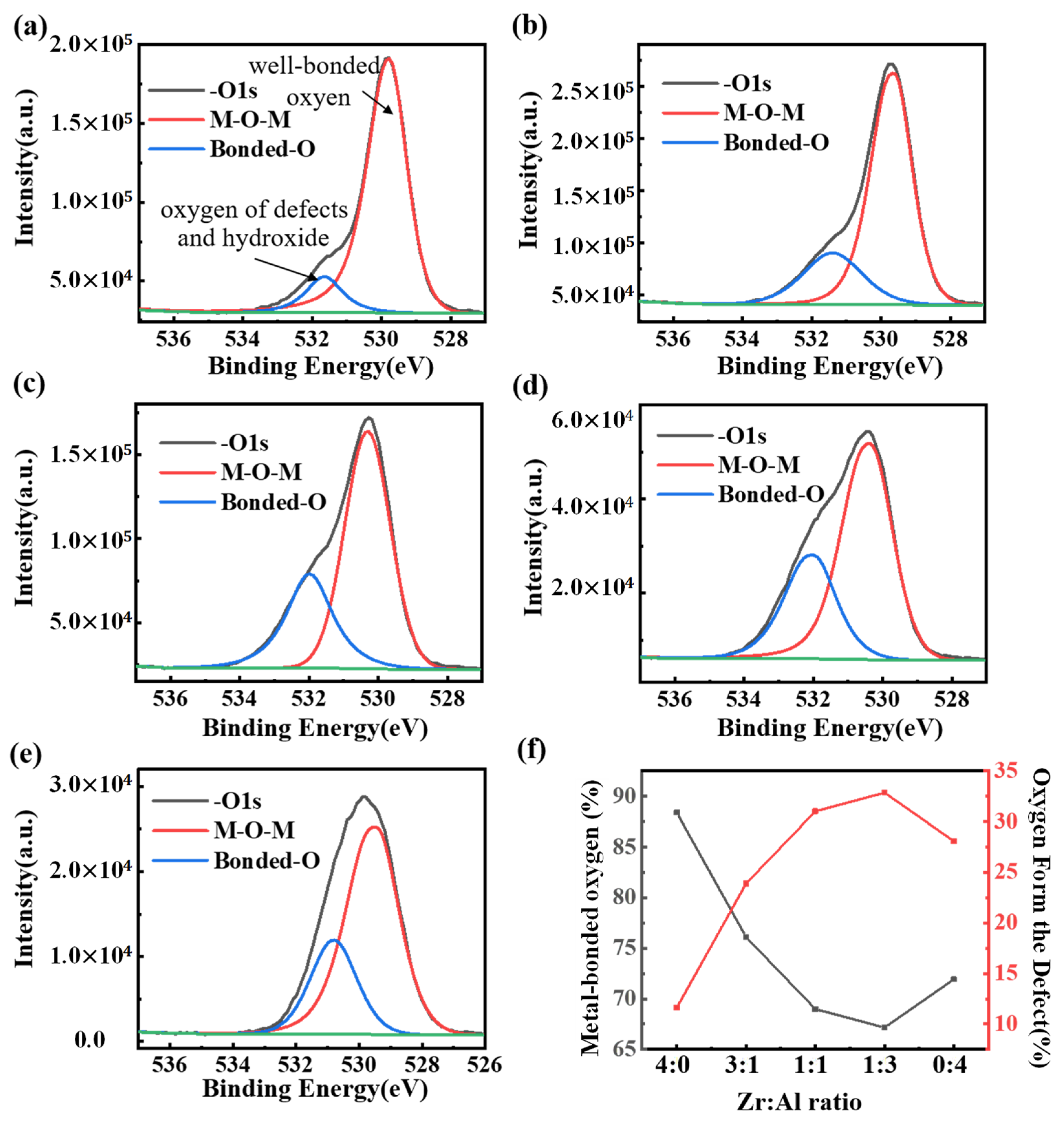
| Molar Ratio Zr:Al | Metal-Bonded Oxygen (~529.5 eV) | Oxygen Form the Lattice Defect (~532 eV) |
|---|---|---|
| 4:0 | 88.37% | 11.63% |
| 3:1 | 76.11% | 23.89% |
| 1:1 | 69.00% | 31.00% |
| 1:3 | 67.16% | 32.84% |
| 0:4 | 71.93% | 28.07% |
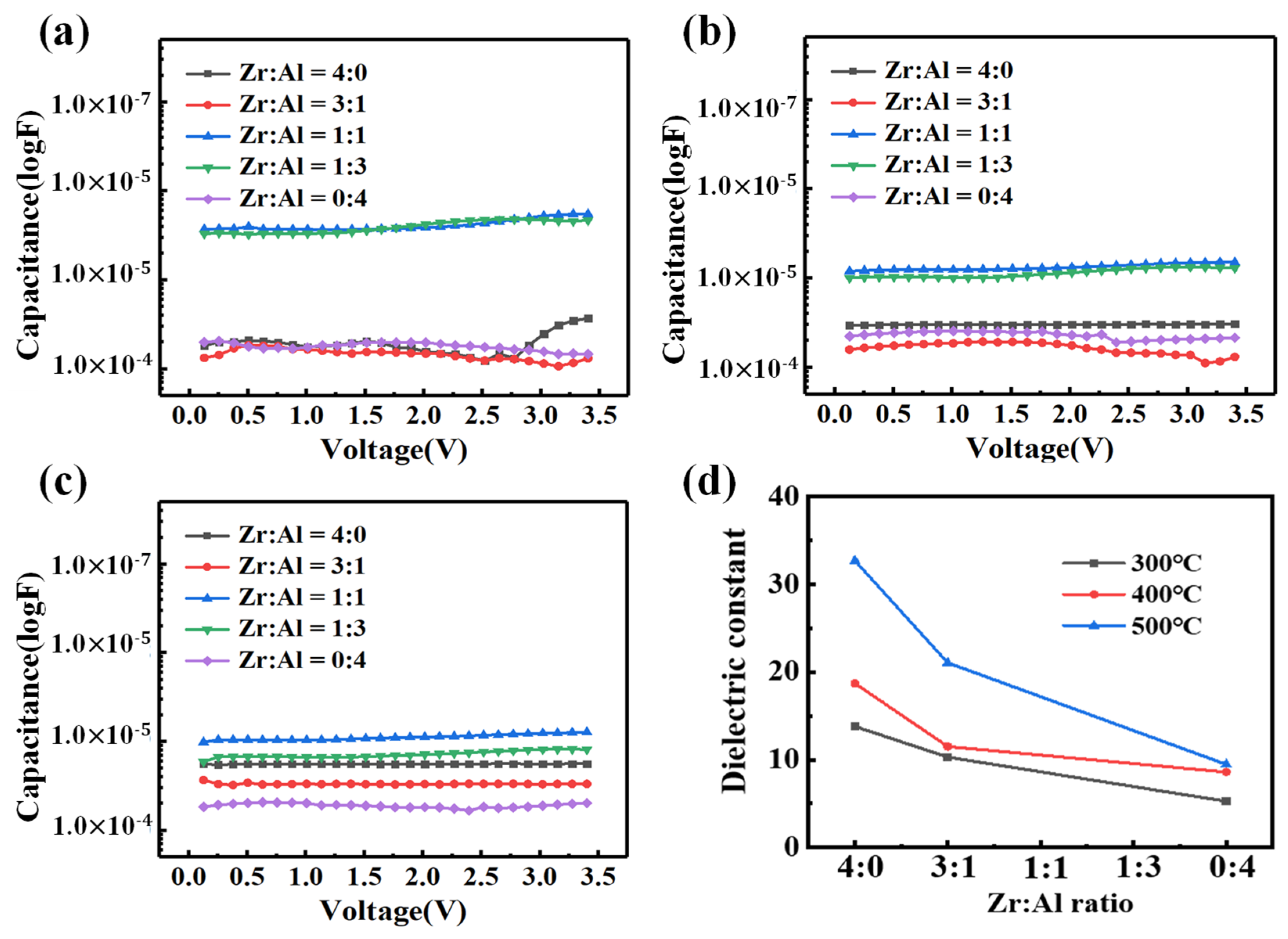
| Molar Ratio Zr:Al | Relative Dielectric Constant at 300 °C | Relative Dielectric Constant at 400 °C | Relative Dielectric Constant at 500 °C |
|---|---|---|---|
| 4:0 | 13.8 | 18.7 | 32.7 |
| 3:1 | 10.3 | 11.5 | 21.1 |
| 1:1 | 292 | 90.5 | 70.5 |
| 1:3 | 277 | 59.3 | 41.1 |
| 0:4 | 5.26 | 8.59 | 9.46 |
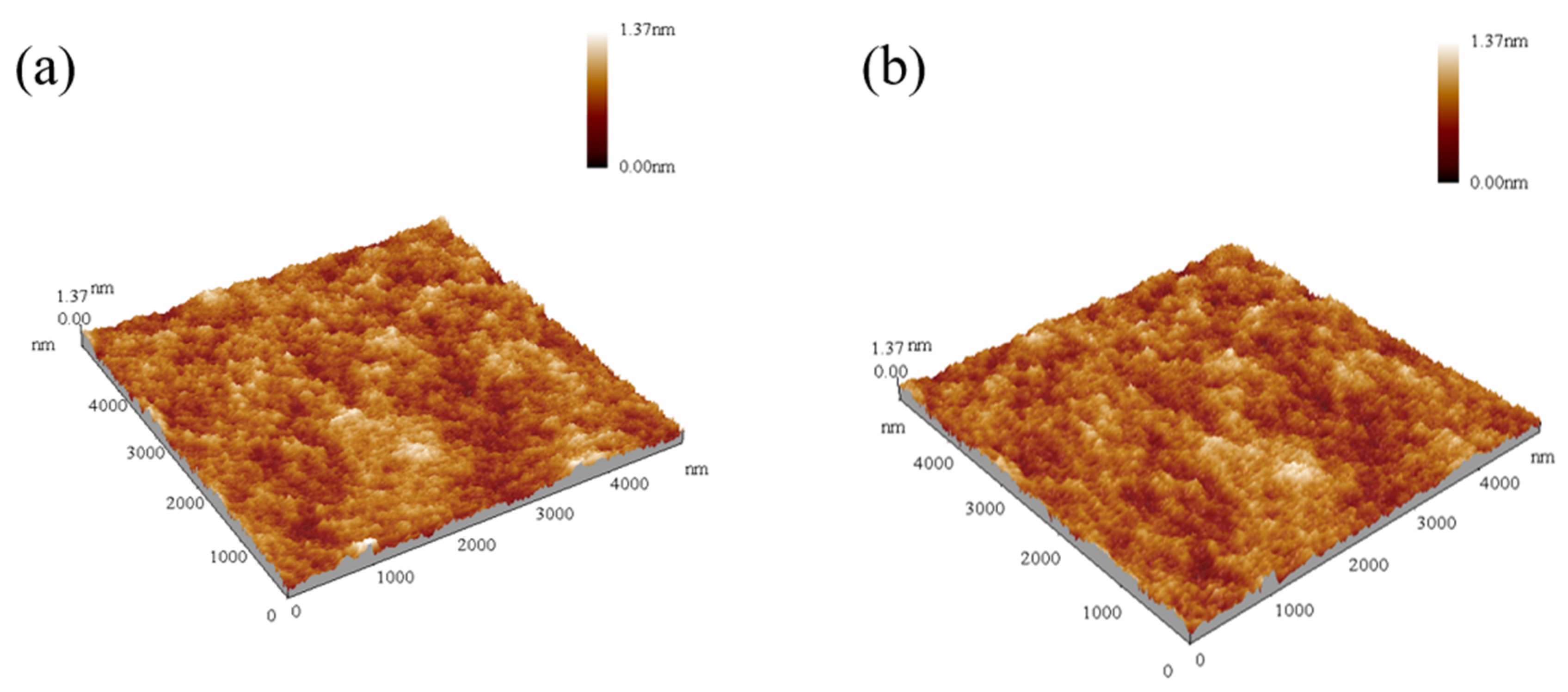
| Molar Ratio Zr:Al | Roughness at 300 °C/nm | Roughness at 400 °C/nm | Roughness at 500 °C/nm |
|---|---|---|---|
| 4:0 | 0.19 | 0.48 | 0.60 |
| 3:1 | 0.30 | 0.14 | 0.15 |
| 1:1 | 0.26 | 0.22 | 0.22 |
| 1:3 | 0.33 | 0.31 | 0.43 |
| 0:4 | 0.31 | 0.37 | 0.30 |
| Molar Ratio Zr:Al | Annealed at 400 °C | Annealed at 500 °C | ||||
|---|---|---|---|---|---|---|
| μsat/cm2/Vs | Ion/off | SS(V/dec) | μsat/cm2/Vs | Ion/off | SS(V/dec) | |
| 4:0 | 1.21 | 1.76 × 10⁷ | 0.131 | 3.57 | 3.5 × 10⁵ | 0.22 |
| 3:1 | 4.23 | 2.2 × 10⁶ | 0.11 | 14.89 | 6.1 × 10⁶ | 0.11 |
| 1:1 | 13.04 | 4.4 × 10³ | 0.98 | 5.67 | 2.73 × 10⁵ | 0.27 |
| 1:3 | 10.18 | 3.5 × 10⁴ | 0.207 | 7.64 | 6.4 × 10⁴ | 0.42 |
| 0:4 | 6.58 | 5.1 × 10⁶ | 0.172 | 8.97 | 1.61 × 10⁷ | 0.35 |
© 2020 by the authors. Licensee MDPI, Basel, Switzerland. This article is an open access article distributed under the terms and conditions of the Creative Commons Attribution (CC BY) license (http://creativecommons.org/licenses/by/4.0/).
Share and Cite
Liang, Z.; Zhou, S.; Cai, W.; Fu, X.; Ning, H.; Chen, J.; Yuan, W.; Zhu, Z.; Yao, R.; Peng, J. Zirconium-Aluminum-Oxide Dielectric Layer with High Dielectric and Relatively Low Leakage Prepared by Spin-Coating and the Application in Thin-Film Transistor. Coatings 2020, 10, 282. https://doi.org/10.3390/coatings10030282
Liang Z, Zhou S, Cai W, Fu X, Ning H, Chen J, Yuan W, Zhu Z, Yao R, Peng J. Zirconium-Aluminum-Oxide Dielectric Layer with High Dielectric and Relatively Low Leakage Prepared by Spin-Coating and the Application in Thin-Film Transistor. Coatings. 2020; 10(3):282. https://doi.org/10.3390/coatings10030282
Chicago/Turabian StyleLiang, Zhihao, Shangxiong Zhou, Wei Cai, Xiao Fu, Honglong Ning, Junlong Chen, Weijian Yuan, Zhennan Zhu, Rihui Yao, and Junbiao Peng. 2020. "Zirconium-Aluminum-Oxide Dielectric Layer with High Dielectric and Relatively Low Leakage Prepared by Spin-Coating and the Application in Thin-Film Transistor" Coatings 10, no. 3: 282. https://doi.org/10.3390/coatings10030282
APA StyleLiang, Z., Zhou, S., Cai, W., Fu, X., Ning, H., Chen, J., Yuan, W., Zhu, Z., Yao, R., & Peng, J. (2020). Zirconium-Aluminum-Oxide Dielectric Layer with High Dielectric and Relatively Low Leakage Prepared by Spin-Coating and the Application in Thin-Film Transistor. Coatings, 10(3), 282. https://doi.org/10.3390/coatings10030282