
Electrical Contact Resistance of Large-Area Graphene on Pre-Patterned Cu and Au Electrodes

 ,
,  ,
, 
Abstract
1. Introduction
2. Materials and Methods
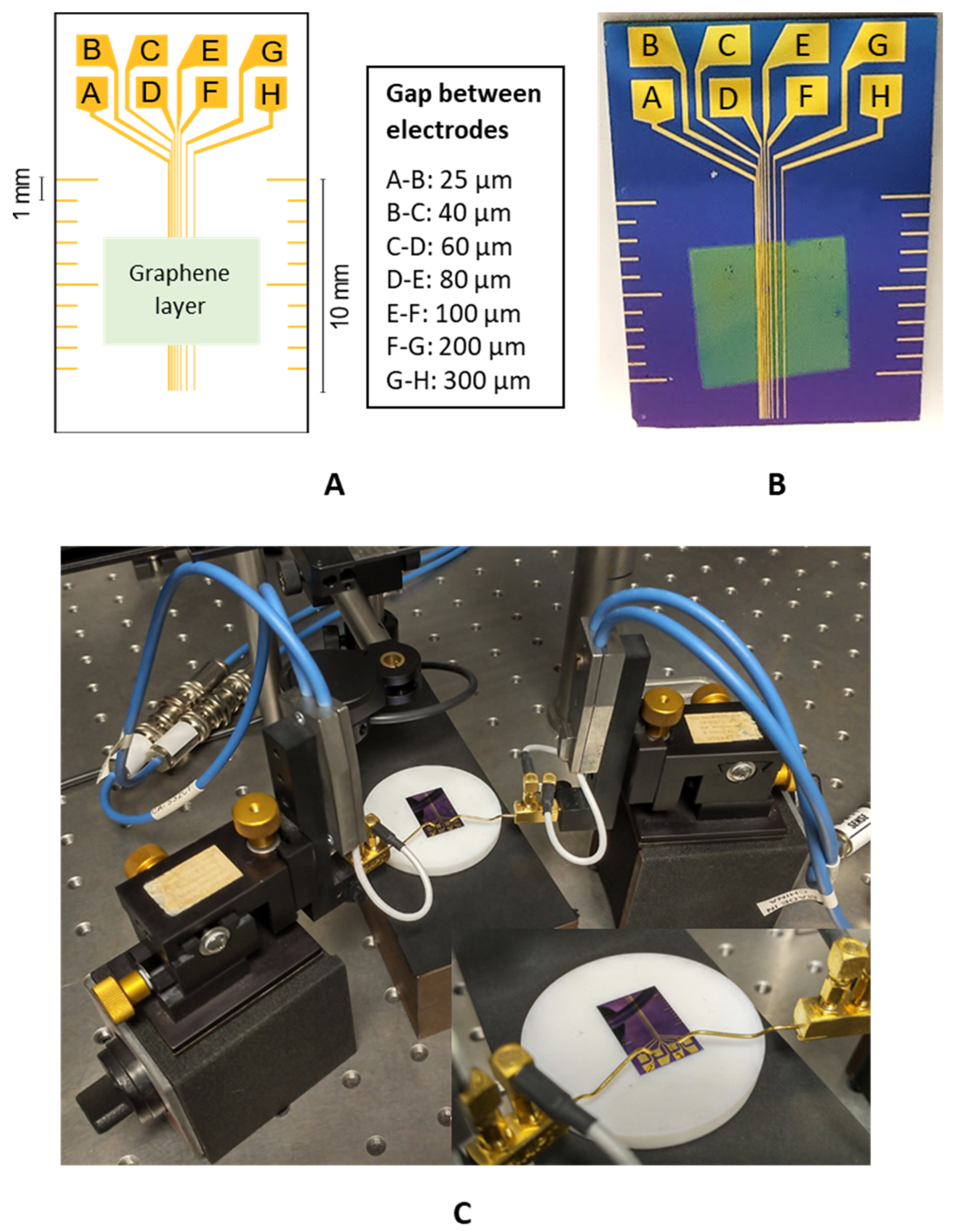
2.1. Materials
2.2. Methods
3. Results and Discussion
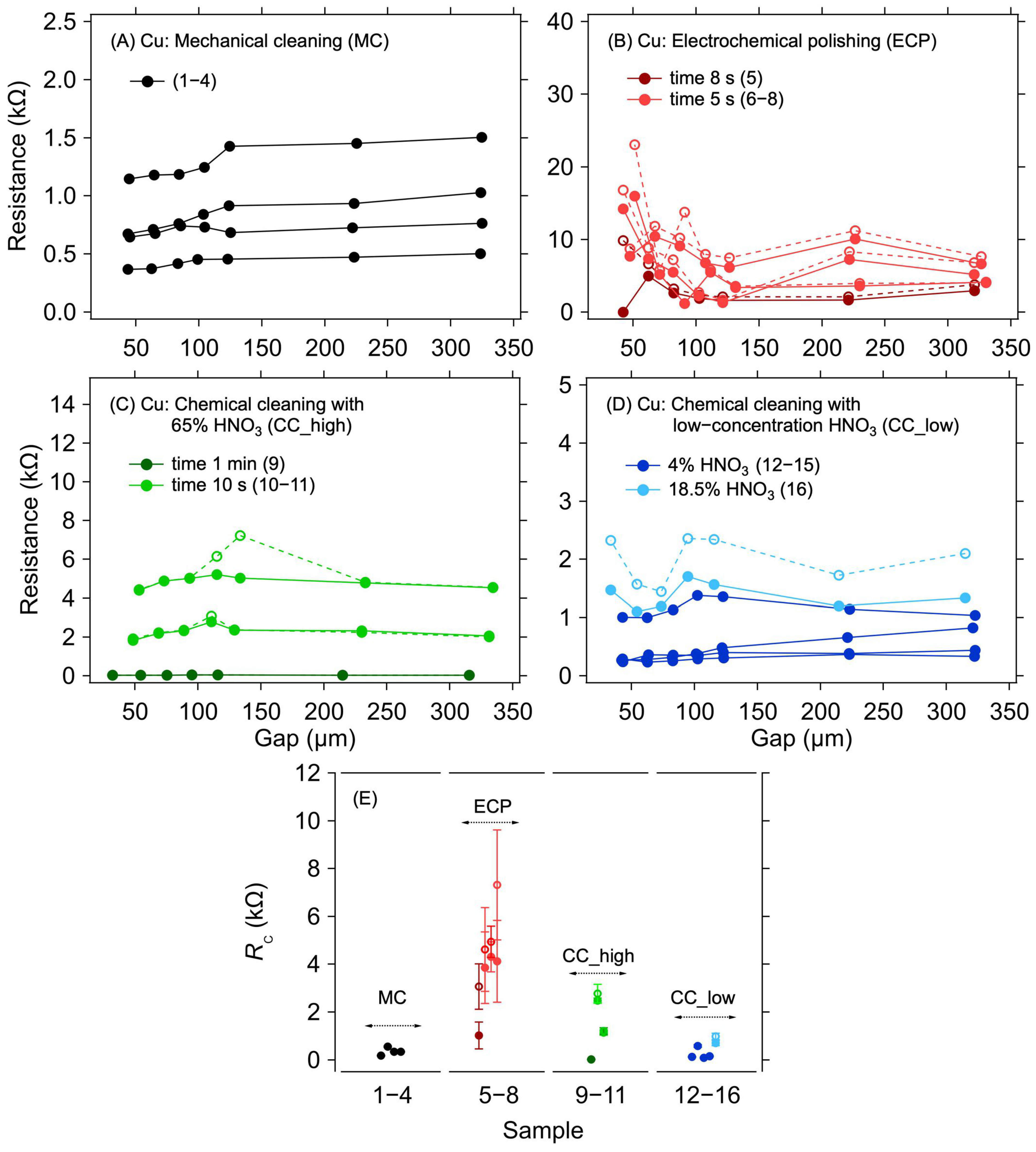
3.1. Cu Electrode System
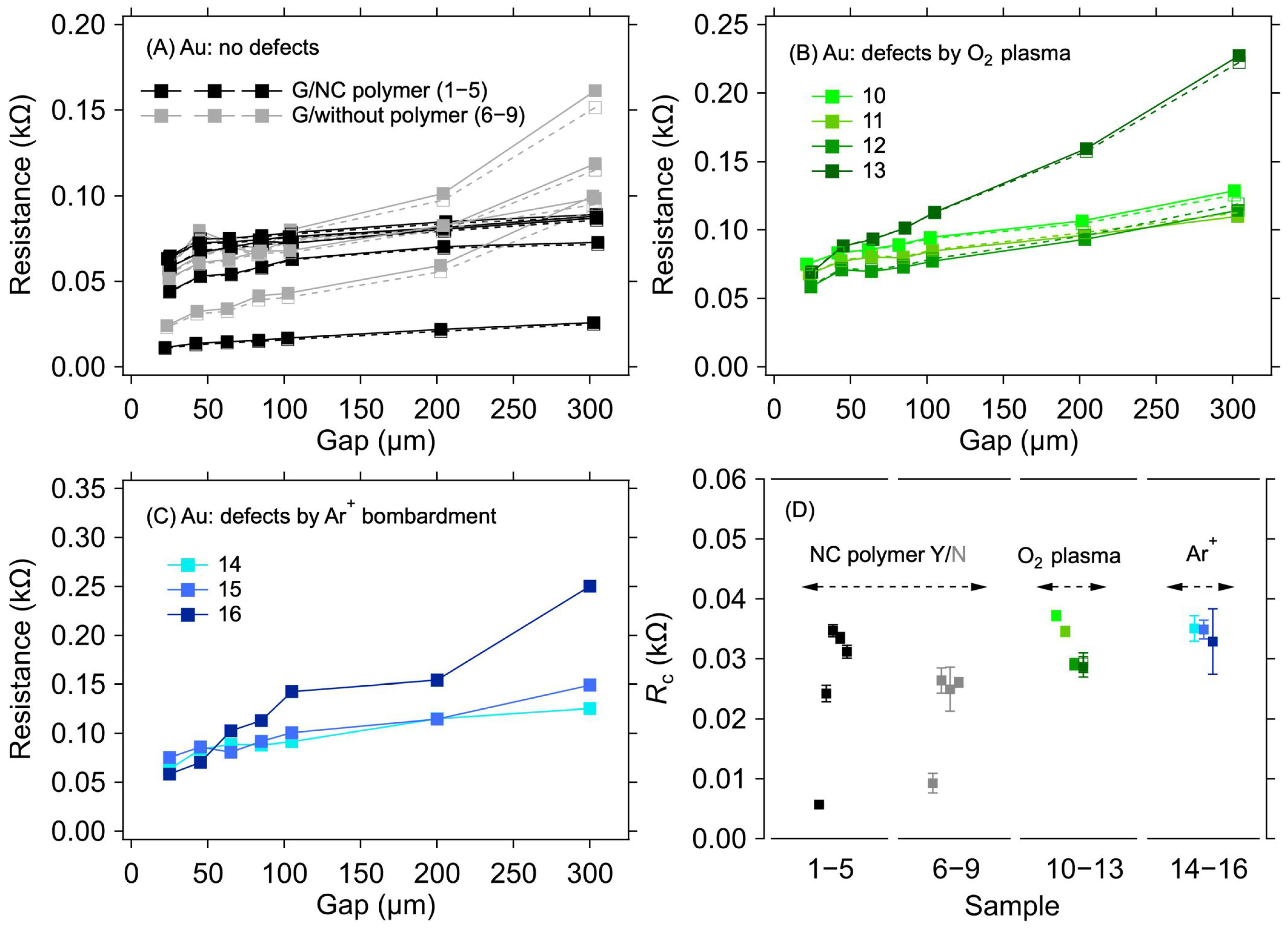
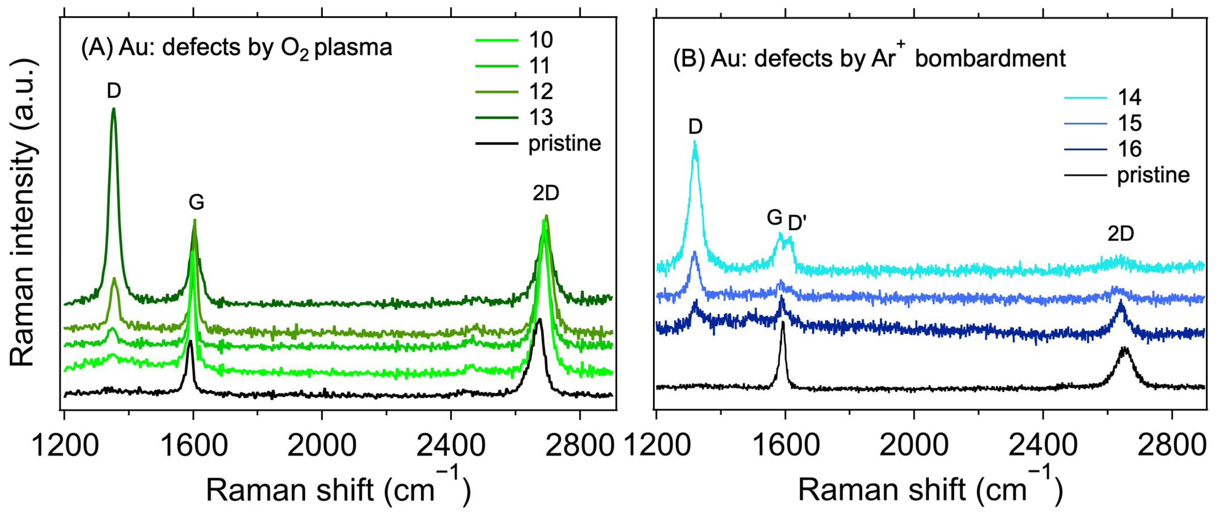
3.2. Au Electrode System
4. Conclusions
Author Contributions
Funding
Data Availability Statement
Conflicts of Interest
References
- Lemme, M.C.; Li, L.-J.; Palacios, T.; Schwierz, F. Two-Dimensional Materials for Electronic Applications. MRS Bull. 2014, 39, 711–718. [Google Scholar] [CrossRef]
- Pereira, P.; Ferreira, D.P.; Araújo, J.C.; Ferreira, A.; Fangueiro, R. The Potential of Graphene Nanoplatelets in the Development of Smart and Multifunctional Ecocomposites. Polymers 2020, 12, 2189. [Google Scholar] [CrossRef] [PubMed]
- Kamedulski, P.; Truszkowski, S.; Lukaszewicz, J.P. Highly Effective Methods of Obtaining N-Doped Graphene by Gamma Irradiation. Materials 2020, 13, 4975. [Google Scholar] [CrossRef] [PubMed]
- Jiménez-Marín, E.; Moreno-Valenzuela, J.; Trejo-Valdez, M.; Martinez-Rivas, A.; Vargas-García, J.R.; Torres-Torres, C. Laser-Induced Electrical Signal Filtering by Multilayer Reduced Graphene Oxide Decorated with Au Nanoparticles. Opt. Express 2019, 27, 7330. [Google Scholar] [CrossRef]
- Islam, M.R.; Shifat, A.S.M.Z.; Liu, K.; Li, Q.; Yang, C.; Wang, Z.; Qu, S.; Wang, Z. Impact of Contact Resistance on the Performances of Graphene Field-Effect Transistor through Analytical Study. AIP Adv. 2021, 11, 045220. [Google Scholar] [CrossRef]
- Giubileo, F.; Di Bartolomeo, A. The Role of Contact Resistance in Graphene Field-Effect Devices. Prog. Surf. Sci. 2017, 92, 143–175. [Google Scholar] [CrossRef]
- Hsu, A.; Wang, H.; Kim, K.K.; Kong, J.; Palacios, T. Impact of Graphene Interface Quality on Contact Resistance and RF Device Performance. IEEE Electron Device Lett. 2011, 32, 1008–1010. [Google Scholar] [CrossRef]
- Passi, V.; Gahoi, A.; Marin, E.G.; Cusati, T.; Fortunelli, A.; Iannaccone, G.; Fiori, G.; Lemme, M.C. Ultralow Specific Contact Resistivity in Metal–Graphene Junctions via Contact Engineering. Adv. Mater. Interfaces 2019, 6, 1801285. [Google Scholar] [CrossRef]
- Robinson, J.A.; LaBella, M.; Zhu, M.; Hollander, M.; Kasarda, R.; Hughes, Z.; Trumbull, K.; Cavalero, R.; Snyder, D. Contacting Graphene. Appl. Phys. Lett. 2011, 98, 053103. [Google Scholar] [CrossRef]
- Nagashio, K.; Nishimura, T.; Kita, K.; Toriumi, A. Contact Resistivity and Current Flow Path at Metal/Graphene Contact. Appl. Phys. Lett. 2010, 97, 143514. [Google Scholar] [CrossRef]
- Gahoi, A.; Kataria, S.; Lemme, M.C. Temperature Dependence of Contact Resistance for Gold-Graphene Contacts. In Proceedings of the 2017 47th European Solid-State Device Research Conference (ESSDERC), Leuven, Belgium, 11–14 September 2017; IEEE: Leuven, Belgium, 2017; pp. 110–113. [Google Scholar]
- Liu, J.; Bao, S.; Wang, X. Applications of Graphene-Based Materials in Sensors: A Review. Micromachines 2022, 13, 184. [Google Scholar] [CrossRef]
- Štulík, J.; Musil, O.; Josefík, F.; Kadlec, P. Graphene-Based Temperature Sensors–Comparison of the Temperature and Humidity Dependences. Nanomaterials 2022, 12, 1594. [Google Scholar] [CrossRef]
- Huang, H.; Su, S.; Wu, N.; Wan, H.; Wan, S.; Bi, H.; Sun, L. Graphene-Based Sensors for Human Health Monitoring. Front. Chem. 2019, 7, 399. [Google Scholar] [CrossRef]
- Shahdeo, D.; Roberts, A.; Abbineni, N.; Gandhi, S. Graphene Based Sensors. In Comprehensive Analytical Chemistry; Elsevier: Amsterdam, The Netherlands, 2020; Volume 91, pp. 175–199. ISBN 978-0-323-85371-2. [Google Scholar]
- Robert, F. Prediction of Contact Length, Contact Pressure and Indentation Depth of Au/Carbon Nanotube Composite Micro Electrical Contact Using Finite Element Modeling. Appl. Surf. Sci. 2019, 489, 470–476. [Google Scholar] [CrossRef]
- Quellmalz, A.; Smith, A.D.; Elgammal, K.; Fan, X.; Delin, A.; Östling, M.; Lemme, M.; Gylfason, K.B.; Niklaus, F. Influence of Humidity on Contact Resistance in Graphene Devices. ACS Appl. Mater. Interfaces 2018, 10, 41738–41746. [Google Scholar] [CrossRef]
- Novoselov, K.S.; Geim, A.K.; Morozov, S.V.; Jiang, D.; Zhang, Y.; Dubonos, S.V.; Grigorieva, I.V.; Firsov, A.A. Electric Field Effect in Atomically Thin Carbon Films. Science 2004, 306, 666–669. [Google Scholar] [CrossRef] [PubMed]
- Berger, C.; Song, Z.; Li, X.; Wu, X.; Brown, N.; Naud, C.; Mayou, D.; Li, T.; Hass, J.; Marchenkov, A.N.; et al. Electronic Confinement and Coherence in Patterned Epitaxial Graphene. Science 2006, 312, 1191–1196. [Google Scholar] [CrossRef] [PubMed]
- Hernandez, Y.; Nicolosi, V.; Lotya, M.; Blighe, F.M.; Sun, Z.; De, S.; McGovern, I.T.; Holland, B.; Byrne, M.; Gun’Ko, Y.K.; et al. High-Yield Production of Graphene by Liquid-Phase Exfoliation of Graphite. Nat. Nanotechnol. 2008, 3, 563–568. [Google Scholar] [CrossRef]
- González, Z.; Acevedo, B.; Predeanu, G.; Axinte, S.M.; Drăgoescu, M.-F.; Slăvescu, V.; Fernandez, J.J.; Granda, M.; Gryglewicz, G.; Melendi-Espina, S. Graphene Materials from Microwave-Derived Carbon Precursors. Fuel Process. Technol. 2021, 217, 106803. [Google Scholar] [CrossRef]
- Li, X.; Cai, W.; An, J.; Kim, S.; Nah, J.; Yang, D.; Piner, R.; Velamakanni, A.; Jung, I.; Tutuc, E.; et al. Large-Area Synthesis of High-Quality and Uniform Graphene Films on Copper Foils. Science 2009, 324, 1312–1314. [Google Scholar] [CrossRef]
- Huet, B.; Raskin, J.-P.; Snyder, D.W.; Redwing, J.M. Fundamental Limitations in Transferred CVD Graphene Caused by Cu Catalyst Surface Morphology. Carbon 2020, 163, 95–104. [Google Scholar] [CrossRef]
- Gahoi, A.; Wagner, S.; Bablich, A.; Kataria, S.; Passi, V.; Lemme, M.C. Contact Resistance Study of Various Metal Electrodes with CVD Graphene. Solid-State Electron. 2016, 125, 234–239. [Google Scholar] [CrossRef]
- Park, K.; Lee, J.; Kim, Y.; Yoon, S.; Yoo, B. Study of Cu Electrochemical Polishing Mechanism with Observation of Water Acceptor Diffusion. Front. Chem. 2021, 9, 763508. [Google Scholar] [CrossRef]
- Kalbac, M.; Frank, O.; Kavan, L. The Control of Graphene Double-Layer Formation in Copper-Catalyzed Chemical Vapor Deposition. Carbon 2012, 50, 3682–3687. [Google Scholar] [CrossRef]
- Bláha, M.; Bouša, M.; Valeš, V.; Frank, O.; Kalbáč, M. Two-Dimensional CVD-Graphene/Polyaniline Supercapacitors: Synthesis Strategy and Electrochemical Operation. ACS Appl. Mater. Interfaces 2021, 13, 34686–34695. [Google Scholar] [CrossRef]
- Melníková-Komínková, Z.; Valeš, V.; Frank, O.; Kalbáč, M. Evolution of the Raman 2D’ Mode in Monolayer Graphene during Electrochemical Doping. Microchem. J. 2022, 181, 107739. [Google Scholar] [CrossRef]
- Hallam, T.; Berner, N.C.; Yim, C.; Duesberg, G.S. Strain, Bubbles, Dirt, and Folds: A Study of Graphene Polymer-Assisted Transfer. Adv. Mater. Interfaces 2014, 1, 1400115. [Google Scholar] [CrossRef]
- Cançado, L.G.; Jorio, A.; Ferreira, E.H.M.; Stavale, F.; Achete, C.A.; Capaz, R.B.; Moutinho, M.V.O.; Lombardo, A.; Kulmala, T.S.; Ferrari, A.C. Quantifying Defects in Graphene via Raman Spectroscopy at Different Excitation Energies. Nano Lett. 2011, 11, 3190–3196. [Google Scholar] [CrossRef]
- Schriver, M.; Regan, W.; Gannett, W.J.; Zaniewski, A.M.; Crommie, M.F.; Zettl, A. Graphene as a Long-Term Metal Oxidation Barrier: Worse Than Nothing. ACS Nano 2013, 7, 5763–5768. [Google Scholar] [CrossRef]
- Liu, N.; Pan, Z.; Fu, L.; Zhang, C.; Dai, B.; Liu, Z. The Origin of Wrinkles on Transferred Graphene. Nano Res. 2011, 4, 996–1004. [Google Scholar] [CrossRef]
- Pacakova, B.; Verhagen, T.; Bousa, M.; Hübner, U.; Vejpravova, J.; Kalbac, M.; Frank, O. Mastering the Wrinkling of Self-Supported Graphene. Sci. Rep. 2017, 7, 10003. [Google Scholar] [CrossRef]
- Ma, B.; Gong, C.; Wen, Y.; Chen, R.; Cho, K.; Shan, B. Modulation of Contact Resistance between Metal and Graphene by Controlling the Graphene Edge, Contact Area, and Point Defects: An Ab Initio Study. J. Appl. Phys. 2014, 115, 183708. [Google Scholar] [CrossRef]
- Anzi, L.; Mansouri, A.; Pedrinazzi, P.; Guerriero, E.; Fiocco, M.; Pesquera, A.; Centeno, A.; Zurutuza, A.; Behnam, A.; Carrion, E.A.; et al. Ultra-Low Contact Resistance in Graphene Devices at the Dirac Point. 2D Mater. 2018, 5, 025014. [Google Scholar] [CrossRef]
- Smith, J.T.; Franklin, A.D.; Farmer, D.B.; Dimitrakopoulos, C.D. Reducing Contact Resistance in Graphene Devices through Contact Area Patterning. ACS Nano 2013, 7, 3661–3667. [Google Scholar] [CrossRef]
- Cusati, T.; Fiori, G.; Gahoi, A.; Passi, V.; Lemme, M.C.; Fortunelli, A.; Iannaccone, G. Electrical Properties of Graphene-Metal Contacts. Sci. Rep. 2017, 7, 5109. [Google Scholar] [CrossRef]
- Vlassiouk, I.; Smirnov, S.; Ivanov, I.; Fulvio, P.F.; Dai, S.; Meyer, H.; Chi, M.; Hensley, D.; Datskos, P.; Lavrik, N.V. Electrical and Thermal Conductivity of Low Temperature CVD Graphene: The Effect of Disorder. Nanotechnology 2011, 22, 275716. [Google Scholar] [CrossRef]
- Shlimak, I.; Haran, A.; Zion, E.; Havdala, T.; Kaganovskii, Y.; Butenko, A.V.; Wolfson, L.; Richter, V.; Naveh, D.; Sharoni, A.; et al. Raman Scattering and Electrical Resistance of Highly Disordered Graphene. Phys. Rev. B 2015, 91, 045414. [Google Scholar] [CrossRef]
- Eckmann, A.; Felten, A.; Verzhbitskiy, I.; Davey, R.; Casiraghi, C. Raman Study on Defective Graphene: Effect of the Excitation Energy, Type, and Amount of Defects. Phys. Rev. B 2013, 88, 035426. [Google Scholar] [CrossRef]
- Eckmann, A.; Felten, A.; Mishchenko, A.; Britnell, L.; Krupke, R.; Novoselov, K.S.; Casiraghi, C. Probing the Nature of Defects in Graphene by Raman Spectroscopy. Nano Lett. 2012, 12, 3925–3930. [Google Scholar] [CrossRef]
- Sundaram, R.S.; Steiner, M.; Chiu, H.-Y.; Engel, M.; Bol, A.A.; Krupke, R.; Burghard, M.; Kern, K.; Avouris, P. The Graphene–Gold Interface and Its Implications for Nanoelectronics. Nano Lett. 2011, 11, 3833–3837. [Google Scholar] [CrossRef]
- Costa, S.D.; Ek Weis, J.; Frank, O.; Kalbac, M. Temperature and Face Dependent Copper–Graphene Interactions. Carbon 2015, 93, 793–799. [Google Scholar] [CrossRef]
- Watanabe, E.; Conwill, A.; Tsuya, D.; Koide, Y. Low Contact Resistance Metals for Graphene Based Devices. Diam. Relat. Mat. 2012, 24, 171–174. [Google Scholar] [CrossRef]


| Sample | Electrode Surface Treatment | RC (kΩ) | ||
|---|---|---|---|---|
| M1 | M2 | |||
| 1 | MC | rubbed with an eraser and cleaned in DI water | 0.188 ± 0.009 | - |
| 2 | 0.561 ± 0.025 | - | ||
| 3 | 0.338 ± 0.019 | - | ||
| 4 | 0.335 ± 0.011 | - | ||
| 5 | ECP | 50% H3PO4/8 s/1V | 1.024 ± 0.56 | 3.073 ± 0.955 |
| 6 | 50% H3PO4/5 s/1V | 3.861 ± 1.500 | 4.618 ± 1.755 | |
| 7 | 4.319 ± 0.635 | 4.945 ± 0.655 | ||
| 8 | 4.131 ± 1.705 | 7.320 ± 2.300 | ||
| 9 | CC_high | 65% HNO3/1 min, wash in DI water for 10 s | 0.022 ± 0.002 | 0.022 ± 0.002 |
| 10 | 65% HNO3/10 s, wash in DI water for 10 s | 2.475 ± 0.108 | 2.781 ± 0.389 | |
| 11 | 1.142 ± 0.111 | 1.214 ± 0.139 | ||
| 12 | CC_low | 4% HNO3/10 s, wash in DI water for 10 s | 0.127 ± 0.011 | - |
| 13 | 0.584 ± 0.059 | - | ||
| 14 | 0.087 ± 0.011 | - | ||
| 15 | 0.150 ± 0.015 | - | ||
| 16 | 18.5% HNO3/1 min, wash in DI water for 10 s, 1M HCl/1 min, and wash in DI water for 10 s | 0.670 ± 0.108 | 0.981 ± 0.139 | |
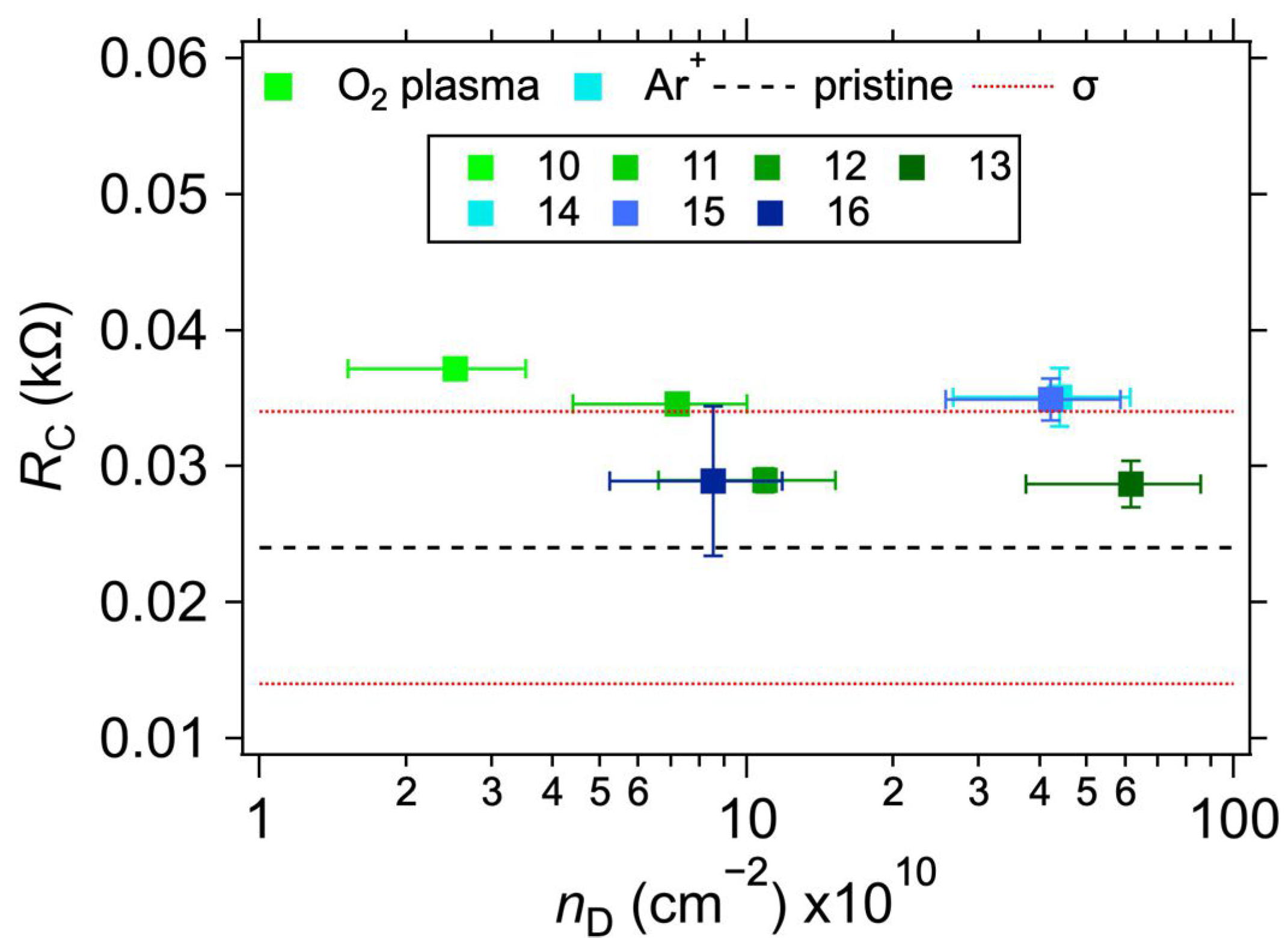
| Sample | Polymer on Top | Defects | ID/IG | LD (nm) | nD (×1010 cm−2) | RC (Ω) | Rs (kΩ/sq) | ||
|---|---|---|---|---|---|---|---|---|---|
| M1 | M2 | ||||||||
| 1 | Yes | No | - | - | 5.7 ± 0.2 | 5.7 ± 0.2 | 0.920 | ||
| 2 | 24.3 ± 1.4 | 24.1 ± 1.3 | 2.588 | ||||||
| 3 | 34.7 ± 1.0 | 34.6 ± 1.0 | 3.031 | ||||||
| 4 | 33.5 ± 0.9 | 33.4 ± 0.9 | 3.074 | ||||||
| 5 | 31.2 ± 1.1 | 31.2 ± 1.0 | 3.052 | ||||||
| 6 | No | 9.3 ± 1.6 | 9.2 ± 1.5 | 2.189 | |||||
| 7 | 26.4 ± 2.1 | 26.3 ± 2.0 | 2.289 | ||||||
| 8 | 25.0 ± 3.7 | 25.2 ± 3.3 | 2.937 | ||||||
| 9 | 26.1 ± 0.7 | 26.0 ± 0.7 | 2.344 | ||||||
| 10 | No | O2 plasma | 12 s/L | 0.11 | 35.5 ± 7.1 | 2.5 ± 1.0 | 37.2 ± 0.7 | 37.3 ± 0.7 | 2.290 |
| 11 | 20 s/L | 0.32 | 20.9 ± 4.2 | 7.2 ± 2.8 | 34.6 ± 0.8 | 34.6 ± 0.8 | 2.173 | ||
| 12 | 10 s/H | 0.48 | 17.1 ± 3.4 | 10.9 ± 4.3 | 29.0 ± 0.9 | 29.1 ± 0.9 | 3.488 | ||
| 13 | 20 s/H | 2.73 | 7.2 ± 1.4 | 61.5 ± 24.1 | 28.7 ± 1.7 | 29.4 ± 1.6 | 2.324 | ||
| 14 | Ar+ bombardment | 3.6 × 1013 cm−2 | 3.94 | 8.5 ± 1.7 | 44.2 ± 17.4 | 35.1 ± 2.1 | - | 2.573 | |
| 15 | 1.2 × 1013 cm−2 | 3.76 | 8.7 ± 1.7 | 42.1 ± 16.5 | 34.9 ± 1.6 | - | 2.476 | ||
| 16 | 4 × 1012 cm−2 | 0.76 | 19.3 ± 3.9 | 8.5 ± 3.3 | 28.9 ± 5.5 | - | 2.362 | ||
Publisher’s Note: MDPI stays neutral with regard to jurisdictional claims in published maps and institutional affiliations. |
© 2022 by the authors. Licensee MDPI, Basel, Switzerland. This article is an open access article distributed under the terms and conditions of the Creative Commons Attribution (CC BY) license (https://creativecommons.org/licenses/by/4.0/).
Share and Cite
Blecha, T.; Vlčková Živcová, Z.; Sonia, F.J.; Mergl, M.; Volochanskyi, O.; Bodnár, M.; Rous, P.; Mizohata, K.; Kalbáč, M.; Frank, O. Electrical Contact Resistance of Large-Area Graphene on Pre-Patterned Cu and Au Electrodes. Nanomaterials 2022, 12, 4444. https://doi.org/10.3390/nano12244444
Blecha T, Vlčková Živcová Z, Sonia FJ, Mergl M, Volochanskyi O, Bodnár M, Rous P, Mizohata K, Kalbáč M, Frank O. Electrical Contact Resistance of Large-Area Graphene on Pre-Patterned Cu and Au Electrodes. Nanomaterials. 2022; 12(24):4444. https://doi.org/10.3390/nano12244444
Chicago/Turabian StyleBlecha, Tomáš, Zuzana Vlčková Živcová, Farjana J. Sonia, Martin Mergl, Oleksandr Volochanskyi, Michal Bodnár, Pavel Rous, Kenichiro Mizohata, Martin Kalbáč, and Otakar Frank. 2022. "Electrical Contact Resistance of Large-Area Graphene on Pre-Patterned Cu and Au Electrodes" Nanomaterials 12, no. 24: 4444. https://doi.org/10.3390/nano12244444
APA StyleBlecha, T., Vlčková Živcová, Z., Sonia, F. J., Mergl, M., Volochanskyi, O., Bodnár, M., Rous, P., Mizohata, K., Kalbáč, M., & Frank, O. (2022). Electrical Contact Resistance of Large-Area Graphene on Pre-Patterned Cu and Au Electrodes. Nanomaterials, 12(24), 4444. https://doi.org/10.3390/nano12244444