Abstract
Hafnium oxide (HfO2) thin film has remarkable physical and chemical properties, which makes it useful for a variety of applications. In this work, HfO2 films were prepared on silicon through plasma enhanced atomic layer deposition (PEALD) at various substrate temperatures. The growth per cycle, structural, morphology and crystalline properties of HfO2 films were measured by spectroscopic ellipsometer, grazing-incidence X-ray diffraction (GIXRD), X-ray reflectivity (XRR), field-emission scanning electron microscopy, atomic force microscopy and x-ray photoelectron spectroscopy. The substrate temperature dependent electrical properties of PEALD–HfO2 films were obtained by capacitance–voltage and current–voltage measurements. GIXRD patterns and XRR investigations show that increasing the substrate temperature improved the crystallinity and density of HfO2 films. The crystallinity of HfO2 films has a major effect on electrical properties of the films. HfO2 thin film deposited at 300 °C possesses the highest dielectric constant and breakdown electric field.
1. Introduction
Hafnium oxide (HfO2) is a promising material for its unique properties, such as high dielectric constant (k), high breakdown electric field, large band gap, excellent surface passivation performance, good stability, high refractive index and wide range of ultraviolet–infrared transparency region [1,2]. As a consequence of these properties, HfO2 film has captivated a tremendous amount of research interest for its applications in a variety of fields, such as anti-reflection films for ultraviolet lasers [3,4], high-k material in capacitors [5,6], non-volatile memories [7] and gate oxide in MOSFETs [8]. HfO2 film has wide applicability to both electronics and optoelectronics. It is used as a high-k material tunnel and gate oxide in nanocrystal floating gate non-volatile memories [9]. HfO2 film is further developed as a ferroelectric material for enhancing the memory windows [2]. HfO2 film also showed great applicability in short-wave infrared photosensors [10]. Furthermore, HfO2 film is utilized as an insulating material in perovskite solar cells [11], Cu(In,Ga)Se2 solar cells [12], c-silicon Passivated Emitter Rear Cell [13] and Polymer solar cells [14]. Due to its multiple applications, great efforts have been devoted to prepare and characterize the HfO2 films. In addition, the performance of HfO2 films is highly determined by the preparation methods. To obtain proper application, preparation of HfO2 film has been investigated through several methods, including ion beam sputtering [15], magnetron sputtering [16,17], molecular beam epitaxy (MBE) [18], metal organic chemical vapor deposition (MOCVD) [19,20], pulsed laser deposition (PLD) [21,22] and atomic layer deposition (ALD). HfO2 films obtained by MBE, MOCVD and PLD need to be prepared at a relatively high substrate temperature. Among these methods, ALD is considered to be one of most hopeful methods owing to its versatile advantages, such as accurate film thickness control, reproducibility, good conformity and high uniformity. ALD is able to meet the needs for atomic layer control and conformal deposition using a sequential, self-limiting surface reaction [23]. ALD is a thin film deposition technique based on the cycle-wise and alternate pulsing of precursor and reactant gases to a reactive surface [24]. ALD can be categorized into thermal ALD and plasma-enhanced ALD (PEALD). Compared with thermal ALD, PEALD offers many advantages, including a lower deposition temperature, a wider choice of feasible precursors and materials, advanced materials properties, more thorough surface ligand removal/regeneration and more flexibility for process optimizations [25]. The improved material properties are a result of the high reactivity provided by the plasma [26]. In PEALD, the surface is exposed to the species generated by a plasma during the reactant step. Typical plasmas used during PEALD are those generated in O2, N2 and H2 reactant gases or combinations thereof [27]. Such plasmas can replace ligand-exchange reactions typical of H2O or NH3 and can be employed to deposit metal oxides, metal nitrides and metal films. The substrate temperature is a key parameter that influences the property of HfO2 films grown by ALD. It determines the surface reaction and transformation of film structure. Therefore, substrate temperature has a critical effect on the crystalline behavior of the HfO2 film and, further, strongly affects the morphological and electrical properties of HfO2 films. Both thermal ALD and PEALD are successfully utilized to deposit HfO2 films. The growth of HfO2 films at various growth temperatures has been investigated by many research groups. In 2015, J. Gao et al. [28] reported that the grown temperature of HfO2 film prepared by thermal ALD must be kept at 200–240 °C to acquire a stable deposition rate of about 1 Å/cycle and the films with higher electric constant. Sai Li et al. [29] investigated structural and optical qualities of HfO2 films through ALD by adjusting the substrate temperature between 170 °C and 290 °C. D. Blaschke et al. [30] studied the hydrogen impurity level in thermal ALD deposited HfO2 films using tetrakis(dimethylamino)hafnium (TDMAHf) precursor and water at the growth temperature between 100 °C and 350 °C. In 2021, Matin Forouzmehr et al. [31] deposited HfO2 films on flexible polymeric substrates at temperatures changing from 100 to 250 °C. Although a lot of effort has been carried out to investigate the stability and interface chemistry of HfO2 films at a variety of temperatures, there exists much less literature about the effects of crystalline behavior on the electrical properties of HfO2 films. Additionally, there is an inalienable relationship between the electrical properties of HfO2 films and substrate temperature. Therefore, the crystalline structure affecting the electrical performance of HfO2 films deposited by PEALD was worthy of further investigation.
In this work, HfO2 films were grown by PEALD on silicon (Si) substrates. The substrate temperature was changed from 100 °C to 450 °C. The substrate temperature on the growth rate, surface morphology, crystalline behavior and electrical properties of the grown HfO2 films was comprehensively studied.
2. Experimental Methods
In this work, 4-inch p type Si wafers with a resistivity of 1–3 Ω·m were utilized as deposition substrates. Si substrates were ultrasonically cleaned by deionized water (10 s), 2% diluted hydrofluoric acid solution (1 min) and deionized water (10 s), respectively. After cleaning, the Si substrates were blown by nitrogen (N2) and transferred to the substrate holder. HfO2 films were prepared on Si at a temperature of 100, 200, 300, 400 and 450 °C using tetrakis (ethylemethylamino) hafnium (TEMAH, purity: 99.9999%, Aimou Yuan, Nanjing, China) and oxygen/argon (O2/Ar) plasma in a PEALD system (Picosun R-200, Espoo, Finland). The plasmas with the mixture of O2 and Ar gases were produced in a microwave cavity by an inductive coupling of radio frequency (RF) power (Litmas RPS, Advanced Energy, Denver, CO, USA). The plasma power was 2500 W. TEMAH was stored at a temperature of 120 °C in a bubbler-type stainless canister. N2 gas was utilized as the carrier gas for TEMAH. Its flow rate is 50 standard cubic centimeters per minute (sccm). The flow rate was controlled by a mass flow controller. The gas lines were heated to 130 °C, higher than the temperature of the bubbler-type stainless canister, to avoid the condensation of precursor. The base pressure of the reactive chamber was 100 Pa. The deposition process of PEALD HfO2 films sequentially included: TEMAH pulse time (1.6 s), N2 purge time (10 s), O2/Ar plasma processing (10 s) and N2 purge time (12 s). The deposition parameters of HfO2 films are listed in Table 1.

Table 1.
Deposition conditions of PEALD HfO2 thin films.
The thicknesses of HfO2 films were measured using spectroscopic ellipsometer (SE, 800 DUV, SENTECH, Berlin, Germany). The crystallinity and mass density of HfO2 films were measured through grazing incidence X-ray diffraction (GIXRD) and X-ray reflectivity (XRR). The diffraction pattern was acquired with an X-ray diffractometer through Cu Kα irradiation with an incident angle of 1°. The initial scan was performed with a 2θ range of 10° to 80° at 0.02° step size and 4 min counting time. The XRR analysis was performed by a diffractometer using parallel beam geometry at an angle of incidence of 0° to 5°. The data analysis was carried out by the software SmartLab Studio II. The fitting model included a HfO2/SiO2/Si stack. The field emission scanning electron microscopy (FESEM, sigma 500, Oberkochen, Germany) and atomic force microscopy (AFM, XE7, Suwon, South Korea) characterizations were carried out to study surface morphology and roughness of HfO2 films. The chemical composition and bonding state in HfO2 films were measured by X-ray photoelectron spectroscopic analysis (XPS, ESCALAB 250Xi, Thermo Fisher, Waltham, MA, USA). Monochromatic Al Kα was used as an X-ray source. The X-ray spot size of 400 μm was detected for HfO2 films analysis. The binding energies were calibrated by a reference of C1s at the peak of 284.8 eV. The surface of HfO2 films was etched through Ar ion beam for 30 s to remove contaminants. The capacitance-voltage (C-V) and current-voltage (I-V) characterizations of HfO2-based devices were performed through a semiconductor parameter measurement system (Keithley 4200-SCS) with an EZON Probe Station at room temperature. For the device’s fabrication, Al/HfO2/Si capacitors were obtained through evaporating circular Aluminum (Al) dots with a metal mask (diameter: ~880 μm). Back contacts were also evaporating Al in a thermal system. Before real measurements, open circuit and short circuit calibration were performed. All the electrical tests were performed in a dark box.
3. Results and Discussion
To identify the growth per cycle (GPC) of HfO2 film, the HfO2 film thicknesses were characterized by SE at different positions. Thickness measurements were carried out after 100, 200, 300, 400 and 500 reaction cycles. Figure 1a presents the thickness of HfO2 films grown at 100, 200, 300, 400 and 450 °C as a function of the number of PEALD cycles. The thickness of HfO2 films increased linearly as the number of PEALD reaction cycles increased. This phenomenon indicated that the GPC is almost constant at each cycle. GPC can be determined from the slope of the linear fitting. Figure 1b illustrates the GPC of HfO2 thin films as a function of different temperatures. The GPC variation can be divided into three regimes. The GPC is approximately 0.13 nm/cycle at a substrate temperature of 100 °C. The GPC decreases to around 0.09 nm/cycle when the substrate temperature was increased to 200 °C. As the substrate temperature increases to 300 °C, the GPC of HfO2 film remains almost constant. Hence, a self-limited window temperature is found at 200–300 °C. When the substrate temperature was increased to 450 °C, the GPC experiences a big jump and reaches a value of 0.18 nm/cycle. The higher GPC at a temperature of 100 °C may result from the precursor of TEMAH condensation or physical adsorption on the surface of the Si substrate under lower temperature [28]. Therefore, when the HfO2 film is deposited at 100 °C, the surface reaction might deviate from the ideal ALD process, resulting in a higher GPC. In this case, the HfO2 films were deposited with a relatively loose structure. When the substrate temperature is varied from 200 °C to 300 °C, the GPC has almost no change, nearly 0.09 nm/cycle, indicating that the GPC of the HfO2 film is considerably stable. This phenomenon, generally called an ALD window, suggests a self-limiting surface reaction behavior. When the substrate temperature goes up to 400 °C and above, the precursor thermally decomposes. This behavior is similar to conventional chemical vapor deposition (CVD). The parasitic CVD-like processes during deposition result in a higher GPC. The CVD-like reaction in depositing HfO2 films at higher temperature was also found by In-Sung PARK et al. [32]. The precursor decomposition lies on the reactor design and process conditions. In this study, it was found that the CVD-like contribution was enhanced at high temperatures. In Ke Xu et al.’s study [33], a surge in the GPC of HfO2 film prepared by thermal ALD occurred beyond 250 °C, which resulted from precursor decomposition. However, according to Ke Xu et al.’s research, when the growth temperature was further increased to 275 °C, GPC decreased conversely, owing to predominant premature thermal decomposition of the precursor.
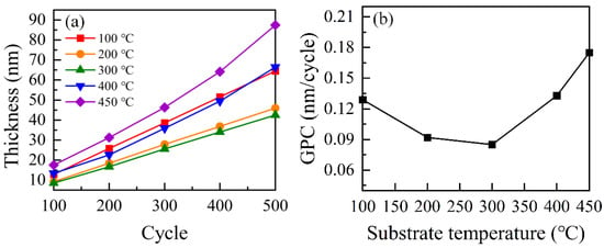
Figure 1.
(a) The thickness of HfO2 film increased linearly with the number of ALD reaction cycles in PEALD. (b) GPC in a temperature range of 100–450 °C.
Figure 2a presents GIXRD patterns of HfO2 films deposited at different substrate temperatures. The GIXRD mode is applied, owing to the thin width of HfO2 films. When the substrate temperature is lower, such as 100 °C and 200 °C, HfO2 films show a broad feature at approximately 2θ of 32°, suggesting that the HfO2 films are amorphous. At lower temperature, the TEMAH and O2/Ar plasma do not have sufficient energy to migrate to the favorable sites. Additionally, the high concentration of physically absorbed precursors may also play a crucial role in generating the amorphous phase, as they may act as a steric hindrance and prevent chemically adsorbed precursors from migrating. When substrate temperature is increased, the precursors obtain more energy and can migrate to the energetically favorable sites. Meanwhile, the steric hindrance deriving from physically adsorbed precursors decreases. As the substrate temperature is further enhanced to 300 °C, some weak diffraction peaks present and the onset of crystallization occurs. Therefore, the HfO2 film transforms from amorphous to crystalline when the substrate temperature is enhanced from 200 °C to 300 °C. The phase transformation from amorphous to crystalline has also been reported by other groups [34]. When substrate temperature is higher than 300 °C, such as 400 °C and 450 °C, HfO2 films display many intense peaks, with different phase orientations which indicate an increase in the degree of crystallization. These peaks are indexed for HfO2 films and are compared with the standard JCPDS (data No. 06-0318) file. It is worth noting that the strongest (−111) phase of HfO2 film deposited at 400 °C transfers to the (200) phase when substrate temperature is increased to 450 °C. The transformation of the strongest phase in HfO2 films may be ascribed to the change in the stress of the films [35]. According to the research by Catalin Palade et al. [36], from HRTEM analysis of the HfO2 films prepared by magnetron sputtering and subjected to rapid thermal annealing, the stress field partially remaining in the lattice induces deformation of monoclinic and tetragonal phases after crystallization. The tetragonal structure formed in the crystal growth process changes into orthorhombic or monoclinic structures by a martensitic-like transition, depending on the doping and local stress field condition. The HfO2 region doped with Ge stabilizes the orthorhombic phase after martensitic-like transformation. Therefore, a transition of the lattice inside crystallites from the monoclinic to orthorhombic phase occurred, accompanied by a continuous strain deformation.
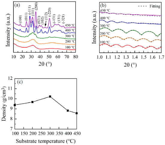
Figure 2.
HfO2 films deposited at 100–450 °C: (a) GIXRD patterns; (b) XRR patterns and measured fitting curves; (c) the extracted density.
The sizes of HfO2 crystallites are obtained according to Scherrer’s formula (1), calculated through the intense (−111) peak data.
where d, k, λ, β and θ refer to the sizes of HfO2 crystallites, the shape factor, the wavelength of X-rays, full width at half maximum (FWHM) and the Bragg’s angle, respectively. The FWHM of the (−111) peak increase is the increasing substrate temperature. The calculated average sizes of HfO2 crystallites decrease accordingly. The sizes of HfO2 crystallites grown at substrate temperatures of 400 °C and 450 °C are approximately 5.1 nm and 4.2 nm, respectively. However, the FWHM of (200) peak decrease is the increasing substrate temperature. Therefore, the calculated sizes of HfO2 crystallites increases, from 5.1 nm at a substrate temperature of 400 °C to 5.2 nm at a substrate temperature of 450 °C.
The increase in crystallization of HfO2 thin films with an increase in substrate temperature also affects the density of ALD–HfO2 films. Figure 2b presents the XRR pattern of HfO2 films deposited at various temperatures. The density of HfO2 films was extracted from the fitted XRR data. Figure 2c presents the density of HfO2 films as a function of substrate temperature. The density of the HfO2 films deposited at 100 °C is about 9.38 g/cm3. When the substrate temperature is raised from 100 °C to 300 °C, the density of HfO2 film increases and approaches the value of approximately 10.22 g/cm3. When the substrate temperature is further increased, the density of the films decreases. Usually, the density of the film depends on the chemical composition and crystallinity. The lower density of HfO2 films may be due to the insufficient surface reaction at a lower substrate temperature [37]. When the substrate temperature is lower, such as 100 °C, more impurities may be involved in the HfO2 film, which possibly derive from the dissociation of precursors. When the substrate temperature is enhanced from 100 °C to 300 °C, impurities in HfO2 films decrease [38]. Additionally, the crystallinity of HfO2 films increases. These two factors cause the improvement in the density of HfO2 films. When the substrate temperature is further enhanced to a higher temperature, the density of HfO2 films deteriorates due to the grain boundary and CVD-like reaction. The highest density of 10.22 g/cm3 obtained in this work is comparable to the reported density of HfO2 film using a MAP-Hf01 precursor and Ar/O2 plasma by Ji-hoon Baaek et al. [39]. The thicknesses of HfO2 films prepared 500 reaction cycles extracted from XRR are 64.7 nm, 46.4 nm,42.2 nm, 66.3 nm and 87.5 nm, respectively.
The surface morphology of HfO2 films at various substrate temperatures was measured by FESEM. The results are displayed in Figure 3. Figure 3a–e presents SEM images of HfO2 films prepared at a temperature of 100, 200, 300, 400 and 450 °C. All the figures have the same amplification factor to obtain a fair comparison. When the substrate temperature is lower, such as 100 °C and 200 °C, the HfO2 films exhibit a smooth surface, indicating a typical amorphous morphology. When the substrate temperature is 300 °C, some grains appear on the surface of the HfO2 film. When the substrate temperature is further raised to a higher value of 400 °C and 450 °C, larger grains with visible grain boundaries are present. Some larger grains might be the clusters consisting of smaller crystallites. The cluster-like surface morphology agrees well with the assumption of thermal decomposition of the TEMAH precursor and the CVD-like grown mode. To further characterize the surface morphological information, AFM measurements were carried out on the surface of the HfO2 films. The AFM images are inset on the top-right corners of the FESEM images. The root mean square (RMS) values obtained from a scan area of 1 μm × 1 μm in tapping mode are plotted in Figure 3f. The RMS value for HfO2 films grown at a substrate temperature of 100 °C is about 0.2 nm. When the substrate temperature rises to 200 °C, the RMS value sees a small increase. However, when the substrate temperature increases to 300 °C, the RMS value experiences a big jump, with a value of approximately 1.4 nm. The roughness of the HfO2 film rapidly increases due to the formation of crystallite [40]. When the substrate temperature further increases up to 400 °C, the RMS value maintains a small increase. When the substrate temperature rises to 450 °C, the RMS value again increases considerably. The surface of HfO2 films becomes rough as the substrate temperature is enhanced from 300 °C to 450 °C. This is attributed to the larger crystal grains embedded in HfO2 films. The AFM characterization of HfO2 films is in good agreement with GIXRD and FESEM measurements of HfO2 films.
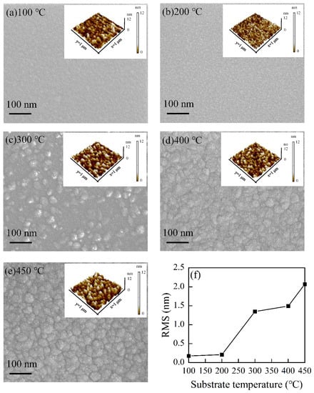
Figure 3.
FESEM and AFM images of HfO2 films with (a) 100 °C, (b) 200 °C, (c) 300 °C, (d) 400 °C and (e) 450 °C. (f) RMS roughness of HfO2 by substrate temperatures.
The XPS characterizations were carried out to study the chemical composition, valence state of Hf, O and relevant defect sites in HfO2 films. Figure 4a presents surveyed XPS spectra of HfO2 films with a binding energy between 1200 and 0 eV. The peaks of Hf and O were investigated in detail. The photoemission intensity peaks Hf 4p1, Hf 4p3, Hf 4d3, Hf 4d5, Hf 4f and O 1s were detected by survey scan, along with auger electron peaks of O KLL. No other contamination species, except carbon, was found within the sensitivity of the instrument. The substrate temperature dependence of the atomic ratio of HfO2 films is plotted in Figure 4b. In all HfO2 films, the Hf atomic ratio was lower than 30% and the O-atomic-ratio was about 65% when compared with the stoichiometric HfO2. The reason for this lies in the carbon content decreasing the Hf atomic ratio. When the substrate temperature was raised from 100 to 450 °C, the O atomic ratio in the HfO2 film is almost constant, while the Hf atomic ratio in HfO2 film increases slightly. There are some carbon (C) impurities in HfO2 films. The carbon atomic ratio in HfO2 film has a decreasing trend except for the film deposited at a temperature of 450 °C. The C 1s atomic ratios in HfO2 films are 7.61%, 6.03%, 4.72%, 3.27% and 3.77%, respectively. The higher carbon concentration at lower substrate temperatures may be ascribed to the incomplete chemical reaction and amorphous structure of HfO2 films. According to the GIXRD measurement, HfO2 films were amorphous when the substrate temperature was lower than 300 °C. In this condition, carbon is more easily adsorbed in HfO2 films. The Hf 4f and O 1s peaks were analyzed in detail. The Hf 4f and O 1s peaks were fitted using the program XPSPEAK4.1 with a Gaussian–Lorentzian mixed function to confirm the chemical composition of HfO2 films. Figure 4c presents high-resolution spectra of Hf 4f of HfO2 films at various substrate temperatures. The Hf 4f spectra can be de-convoluted into two sets of double-peak components. One set of double-peak components at a binding energy of 17.2 eV and 18.8 eV is assigned to Hf4+ 4f7/2 and Hf4+ 4f5/2 peaks of the Hf oxide bond (O-Hf-O), respectively. Another set of double-peak components at a binding energy of 16.5 eV and 18.2 eV is assigned to Hfx+ 4f7/2 (x < 4) and Hfx+ 4f5/2 peaks of Hf suboxide bond, respectively [41]. The double-peak components of oxidized Hf4+ are stronger than those of the sub-oxidized Hfx+. The substrate temperature dependence of the area ratio of Hfx+/(Hfx+ + Hf4+) is plotted in Figure 4d. As the substrate temperature increases from 100 °C to 200 °C, the content of sub-oxidized Hfx+ for the HfO2 film decreases sharply. The content of sub-oxidized Hfx+ for the film remains nearly constant when the substrate temperature is between 200 °C and 300 °C. When the substrate temperature further rises up to 400 °C, the area ratio of Hfx+/(Hfx+ + Hf4+) increases significantly again. The higher content of Hfx+ for the film deposited at 100 °C could be ascribed to the relative shortage of the chemically absorbed precursors owing to the low energy at a low substrate temperature. Many defects, such as carbon and hydroxyl groups, are in the film, while the higher content of Hfx+ for the films deposited at 400 °C and 450 °C may be ascribed to thermal decomposition of the TEMAH precursor at high substrate temperatures. Figure 4e presents the high-resolution spectra of O 1s of HfO2 films at a variety of substrate temperatures. The peaks of O 1s for HfO2 films grown at the lower temperature of 100 °C and higher temperatures of 400–450 °C shift to higher binding energy. This phenomenon could be ascribed to more defects existing in the prepared films. The O 1s spectra can be de-convoluted into two components. The two components at the binding energy of around 530.5 eV and 531.5 eV indicate lattice oxygen (OL) and non-lattice oxygen (ONL), respectively. The OL demonstrates that the prepared films have ordered structures with good properties. The ONL demonstrates that non-lattice oxygen exists in the prepared films, which may originate from the suboxides with Hf [41], O-H or absorbed water. In order to investigate the amount of oxygen vacancies in HfO2 film, the area ratio of ONL/(ONL + OL) as a function of substrate temperature is plotted in Figure 4f. The variation in the area ratio of ONL/(ONL + OL) is similar to the variation in the area ratio of Hfx+/(Hfx+ + Hf4+). When the substrate temperature rises from 100 °C to 300 °C, the area ratio of ONL/(ONL + OL) continuously decreases, indicating more perfect HfO2 lattice. This behavior is caused by the fact that the ratio of chemically adsorbed precursors increases and, therefore, more oxygen atoms can participate in forming Hf-O bonds owing to the increasing reaction energy. When the substrate temperature further increases to 400 °C and 450 °C, the area ratio of ONL/(ONL + OL) increases to higher values of 28.6% and 28.3%. This behavior is possibly attributed to the decomposition of precursors at higher temperature.
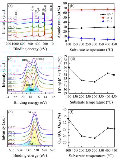
Figure 4.
(a) XPS spectra of HfO2 films with a binding energy between 1200 and 0 eV. (b) Content proportion of Hf, O and C in HfO2 with different substrate temperatures. (c) High-resolution Hf 4f spectra of HfO2 films with various substrate temperatures. (d) The area ratio of Hfx+/(Hfx+ + Hf4+) as a function of substrate temperatures. (e) High-resolution O 1s spectra of HfO2 films with various substrate temperatures. (f) The area ratio of ONL/(ONL + OL) as a function of substrate temperature.
C-V measurements are usually utilized to study the electrical property of dielectric films. C-V measurements were performed herein at room temperature, with the frequency of 1MHz on a standard Al/HfO2/Si/Al structure. Figure 5a illustrates normalized C-V characteristics of HfO2 thin films with various substrate temperatures. The applied voltage (VA) was varied (−6 V < VA < 6V), with a sweep step length of 0.1 V, varying from accumulation to inversion. The variation in C-V curves toward negative voltages indicates the presence of effective oxide charges with positive polarity in prepared HfO2 films. Figure 5b presents the substrate temperature dependence of k of HfO2 films. The extracted k is identified by the maximum capacitance in the accumulation region. The k value is estimated by the following equation
where is the maximum capacitance in the accumulation region, is the area of the capacitor, is the thickness of the HfO2 film and is the dielectric constant of the vacuum. The thickness of HfO2 films used for extracting the dielectric constant is approximately 30 nm. As can be seen in Figure 5b, the value of the HfO2 film increases as the substrate temperature increases from 100 °C to 300 °C. According to the GIXRD measurement, the HfO2 film is mostly amorphous. The lower k value in the lower temperature range is due to the weaker energy of the precursor’s reaction at a lower substrate temperature, resulting in more defects in the prepared film. As the substrate temperature further increases from 300 °C to 450 °C, the k value of the HfO2 film decreases. According to the GIXRD measurement, the HfO2 film’s crystallization becomes obvious when the substrate temperature rises from 300 °C to 450 °C. The defects in crystallized HfO2 films are easily segregated at grain boundaries with unstable bonding, generating a leakage current path, leading to a decrease in k value [42]. Additionally, the decrease in k value in higher substrate temperatures may be ascribed to poor interface property, as presented in C-V curves. The lower slope of C-V curves for the capacitors of HfO2 film prepared at 400 °C and 450 °C indicates that more defects were presented in the interface of HfO2 films and Si substrates.
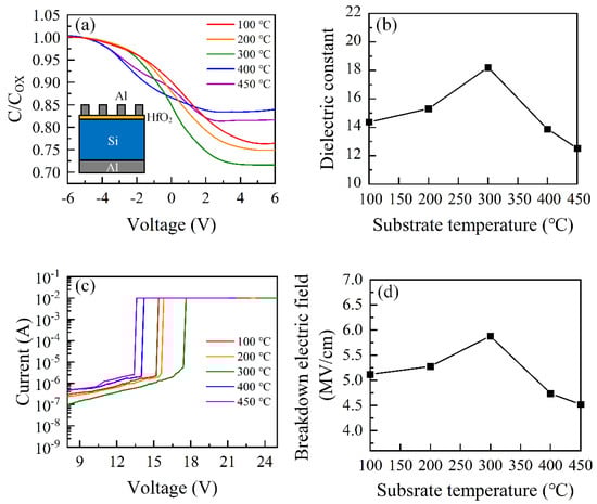
Figure 5.
(a) C-V behavior of HfO2 MOS capacitors. (b) The extracted dielectric constant as a function of substrate temperature. (c) I-V curves of HfO2 MOS capacitors. (d) The breakdown electric field of the HfO2 MOS capacitor according to substrate temperature.
I-V measurements were performed to explore the leakage current properties of Al/HfO2/Si devices. Figure 5c presents I-V curves of the devices at different substrate temperatures. The corresponding breakdown electric field as a function of substrate temperature is also plotted in Figure 5d. As can be seen in the figure, the breakdown electric field firstly increases and then decreases as the substrate temperature increases. When the substrate temperature was 300 °C, the devices obtained the highest breakdown electric field, with the value of 5.88 MV/cm. The decreasing value of the breakdown electric field for the devices prepared at the temperatures higher than 300 °C may be ascribed to the highly crystallized HfO2 films that have a percolation path under the high electrical field due to the high density of the grain boundary defects [39]. The variation in the breakdown electric field is similar to the variation in k. This behavior is caused by the approximate breakdown electric field, Ebd ~ (k)−1/2 relation, illustrated by J. McPherson et al. [43].
Table 2 compares the qualities of HfO2 films obtained by different methods. All of the extracted k values of HfO2 films at various substrate temperatures agree with the reported ALD-grown HfO2 film. In this study, the highest obtained k value of 18.21 at the substrate temperature of 300 °C is higher than most of the other reported PEALD-grown HfO2 films [39,44,45], although it is slightly lower than the k value of 18.60 [46] prepared by PEALD with post deposition annealing and 18.3 [47] prepared by high power impulse magnetron sputtering (HIPIMS). The data of the breakdown electric field and density are not provided in references [46,47]. Therefore, further comparison is not possible. The k values prepared by Young Bum Yoo et al. [48] and Junhui Weng et al. [49] using spin-coating were 14.1 and 16.5, respectively. The k values obtained by Madhuchhanda Nath et al. [50] and A M Lepadatu [9] using radio frequency sputtering were 14 and 15, respectively. The k value obtained by Grzegorz Lupina et al. [51] is 16. The k values obtained by Devika Choudhury et al. [52] and Md. Mamunur Rahman et al. [53] using thermal ALD were 13 and 16.64, respectively. The highest breakdown electric field of the HfO2 films obtained in this work is 5.88 MV/cm, which is slightly lower than the value of 6.2 prepared by Young Bum Yoo et al. [48] using spin-coating. However, it is superior to most of the data provided by the comparative references. The highest density of 10.22 g/cm3 in this work is higher than other values of listing references. According to the investigation of the comparative table, the HfO2 film deposited in this study had a relatively higher mass density and lower defects density. Therefore, a high k value and breakdown electric field can be achieved.
Table 2.
The Comparison of important parameters under different preparation methods.
4. Conclusions
In summary, HfO2 films have been successfully fabricated by PEALD at substrate temperatures ranging from 100 °C to 450 °C. The dependence of crystallization, film density and the electrical property of HfO2 films on substrate temperature has been systematically studied. GIXRD and XRR investigations revealed a gradual phase transformation from an amorphous structure to a polycrystalline structure and a higher crystallization at a substrate temperature of 400 °C. The substrate temperature has a major influence on the film density. XPS results indicate that HfO2 film grown at substrate temperatures of 300 °C has a sufficient chemical reaction, resulting in less Hf suboxide bonds and more lattice oxygen. Additionally, the phase transformation and the grain size of HfO2 films have a tremendous effect on the dielectric constant and breakdown electric field. HfO2 film prepared at 300 °C possesses the highest k value of 18.21 and a breakdown electric field of 5.88 MV/cm.
Author Contributions
Conceptualization, X.-Y.Z., Y.-J.R., D.-S.W., S.-Y.L. and W.-Z.Z.; Data curation, J.H., D.-C.P., W.-Y.W., D.-S.W. and W.-Z.Z.; Formal analysis, Y.-J.R. and C.-J.H.; Funding acquisition, X.-Y.Z., J.H., D.-C.P. and S.-Y.L.; Investigation, W.-Y.W.; Methodology, X.-Y.Z., J.H. and D.-C.P.; Project administration, S.-Y.L.; Writing—original draft, X.-Y.Z. and J.H.; Writing—review & editing, X.-Y.Z. and S.-Y.L. All authors have read and agreed to the published version of the manuscript.
Funding
This work is partially sponsored by the Natural Science Foundation of Fujian Province (Nos. 2020H0025 and 2020J01298), the Science and Technology Project of Xiamen (No. 3502ZCQ20191002), the Xiamen Scientific Research Start-up Foundation for the Returned Overseas Chinese Scholars (No. 5010320004) and the Graduate Science and Technology Innovation Program (No. YKJCX2021102 and YKJCX2021106). This work is also sponsored by the Science and Technology Projects of Fujian Administration for Market Regulation (FJMS2020044).
Data Availability Statement
The data is available on reasonable request from the corresponding author.
Conflicts of Interest
The authors declare that they have no competing interest.
References
- Fina, I.; Sánchez, F. Epitaxial Ferroelectric HfO2 Films: Growth, Properties, and Devices. ACS Appl. Electron. Mater. 2021, 3, 1530–1549. [Google Scholar] [CrossRef]
- Schroeder, U.; Park, M.H.; Mikolajick, T.; Hwang, C.S. The Fundamentals and Applications of Ferroelectric HfO2. Nat. Rev. Mater. 2022, 7, 653–669. [Google Scholar] [CrossRef]
- Yin, C.; Zhu, M.; Zeng, T.; Song, C.; Chai, Y.; Shao, Y.; Zhang, R.; Zhao, J.; Li, D.; Shao, J. HfO2/SiO2 Anti-Reflection Films for UV Lasers via Plasma-Enhanced Atomic Layer Deposition. J. Alloys Compd. 2021, 859, 157875. [Google Scholar] [CrossRef]
- Falmbigl, M.; Godin, K.; George, J.; Mühlig, C.; Rubin, B. Effect of Annealing on Properties and Performance of HfO2 /SiO2 Optical Coatings for UV-Applications. Opt. Express 2022, 30, 12326. [Google Scholar] [CrossRef] [PubMed]
- Singh, S.; Singh, S. Analog/RF Performance Projection of Ultra-Steep Si Doped HfO2 Based Negative Capacitance Electrostatically Doped TFET: A Process Variation Resistant Design. Silicon 2022, 14, 4865–4877. [Google Scholar] [CrossRef]
- Sun, N.; Zhou, D.; Liu, W.; Zhang, Y.; Li, S.; Wang, J.; Ali, F. Importance of Tailoring the Thickness of SiO2 Interlayer in the Observation of Ferroelectric Characteristics in Yttrium Doped HfO2 Films on Silicon. Vacuum 2021, 183, 109835. [Google Scholar] [CrossRef]
- Yun, M.J.; Lee, D.; Kim, S.; Wenger, C.; Kim, H.-D. A Nonlinear Resistive Switching Behaviors of Ni/HfO2/TiN Memory Structures for Self-Rectifying Resistive Switching Memory. Mater. Charact. 2021, 182, 111578. [Google Scholar] [CrossRef]
- Ren, Z.; Lv, D.; Xu, J.; Su, K.; Zhang, J.; Wang, D.; Wu, Y.; Zhang, J.; Hao, Y. Performance of H-Diamond MOSFETs with High Temperature ALD Grown HfO2 Dielectric. Diam. Relat. Mater. 2020, 106, 107846. [Google Scholar] [CrossRef]
- Lepadatu, A.M.; Palade, C.; Slav, A.; Maraloiu, A.V.; Lazanu, S.; Stoica, T.; Logofatu, C.; Teodorescu, V.S.; Ciurea, M.L. Single Layer of Ge Quantum Dots in HfO2 for Floating Gate Memory Capacitors. Nanotechnology 2017, 28, 175707. [Google Scholar] [CrossRef]
- Palade, C.; Lepadatu, A.-M.; Slav, A.; Teodorescu, V.S.; Stoica, T.; Ciurea, M.L.; Ursutiu, D.; Samoila, C. Nanocrystallized Ge-Rich SiGe-HfO2 Highly Photosensitive in Short-Wave Infrared. Materials 2021, 14, 7040. [Google Scholar] [CrossRef]
- Vildanova, M.F.; Nikolskaia, A.B.; Kozlov, S.S.; Shevaleevskiy, O.I. Charge Transfer Mechanisms in Multistructured Photoelectrodes for Perovskite Solar Cells. J. Phys. Conf. Ser. 2020, 1697, 012187. [Google Scholar] [CrossRef]
- Löckinger, J.; Nishiwaki, S.; Bissig, B.; Degutis, G.; Romanyuk, Y.E.; Buecheler, S.; Tiwari, A.N. The Use of HfO2 in a Point Contact Concept for Front Interface Passivation of Cu(In,Ga)Se2 Solar Cells. Sol. Energy Mater. Sol. Cells 2019, 195, 213–219. [Google Scholar] [CrossRef]
- Jha, R.K.; Singh, P.; Goswami, M.; Singh, B.R. Impact of HfO 2 as a Passivation Layer in the Solar Cell Efficiency Enhancement in Passivated Emitter Rear Cell Type. J. Nanosci. Nanotechnol. 2020, 20, 3718–3723. [Google Scholar] [CrossRef]
- Huang, C.; Yu, H. High Performance Polymer Solar Cells Based HfO2 Passivated 2D-HfX2 (X S, Se) as a Hole Transport Layers. Nano Energy 2022, 103, 107750. [Google Scholar] [CrossRef]
- Bendova, M.; Pytlicek, Z.; Prasek, J.; Mozalev, A. The Growth and Unique Electronic Properties of the Porous-Alumina-Assisted Hafnium-Oxide Nanostructured Films. Electrochim. Acta 2019, 327, 135029. [Google Scholar] [CrossRef]
- Zahoor, A.; Xu, C.; Shahid, T.; Anwar, M.A.; Song, Z. Effects of O2 Flux on Structure, Optical Properties and Hydrophobicity of Highly Emissive Antireflective HfO2 Thin Films by Magnetron Sputtering. Vacuum 2022, 197, 110824. [Google Scholar] [CrossRef]
- Dhanunjaya, M.; Manikanthababu, N.; Ojha, S.; Pojprapai, S.; Pathak, A.P.; Nageswara Rao, S.V.S. Effects of Growth Parameters on HfO2 Thin-Films Deposited by RF Magnetron Sputtering. Radiat. Eff. Defects Solids 2022, 177, 15–26. [Google Scholar] [CrossRef]
- Wan, H.W.; Lin, Y.H.; Lin, K.Y.; Chang, T.W.; Cai, R.F.; Kwo, J.; Hong, M. Ultra-High Thermal Stability and Extremely Low D on HfO2/p-GaAs(001) Interface. Microelectron. Eng. 2017, 178, 154–157. [Google Scholar] [CrossRef]
- Vendra, S.S.L.; Antony, N.; Koroleva, E.; Filimonov, A.; Vakhrushev, S.; Kumar, R. Space-Charge Polarisation Dielectric Behaviour of Precursor Derived Monoclinic HfO2. Ceram. Int. 2022, 48, 13063–13070. [Google Scholar] [CrossRef]
- Stesmans, A.; Afanas’ev, V.V. Defect Correlated with Positive Charge Trapping in Functional HfO2 Layers on (100)Si Revealed by Electron Spin Resonance: Evidence for Oxygen Vacancy? Microelectron. Eng. 2017, 178, 112–115. [Google Scholar] [CrossRef]
- Luo, Y.; Tang, Z.; Yin, X.; Chen, C.; Fan, Z.; Qin, M.; Zeng, M.; Zhou, G.; Gao, X.; Lu, X.; et al. Ferroelectricity in Dopant-Free HfO2 Thin Films Prepared by Pulsed Laser Deposition. J. Materiomics 2022, 8, 311–318. [Google Scholar] [CrossRef]
- Nand, M.; Tripathi, S.; Rajput, P.; Kumar, M.; Kumar, Y.; Mandal, S.K.; Urkude, R.; Gupta, M.; Dawar, A.; Ojha, S.; et al. Different Polymorphs of Y Doped HfO2 Epitaxial Thin Films: Insights into Structural, Electronic and Optical Properties. J. Alloys Compd. 2022, 928, 167099. [Google Scholar] [CrossRef]
- George, S.M. Atomic Layer Deposition: An Overview. Chem. Rev. 2010, 110, 111–131. [Google Scholar] [CrossRef] [PubMed]
- Weber, M.J.; Verheijen, M.A.; Bol, A.A.; Kessels, W.M.M. Sub-Nanometer Dimensions Control of Core/Shell Nanoparticles Prepared by Atomic Layer Deposition. Nanotechnology 2015, 26, 094002. [Google Scholar] [CrossRef]
- Chang, J.; Chang, J.P. Achieving Atomistic Control in Materials Processing by Plasma–Surface Interactions. J. Phys. Appl. Phys. 2017, 50, 253001. [Google Scholar] [CrossRef]
- Profijt, H.B.; Potts, S.E.; van de Sanden, M.C.M.; Kessels, W.M.M. Plasma-Assisted Atomic Layer Deposition: Basics, Opportunities, and Challenges. J. Vac. Sci. Technol. Vac. Surf. Films 2011, 29, 050801. [Google Scholar] [CrossRef]
- Weber, M.J.; Mackus, A.J.M.; Verheijen, M.A.; Longo, V.; Bol, A.A.; Kessels, W.M.M. Atomic Layer Deposition of High-Purity Palladium Films from Pd(Hfac)2 and H2 and O2 Plasmas. J. Phys. Chem. C 2014, 118, 8702–8711. [Google Scholar] [CrossRef]
- Gao, J.; He, G.; Zhang, J.W.; Liu, Y.M.; Sun, Z.Q. Deposition Temperature Dependent Optical and Electrical Properties of ALD HfO2 Gate Dielectrics Pretreated with Tetrakisethylmethylamino Hafnium. Mater. Res. Bull. 2015, 70, 840–846. [Google Scholar] [CrossRef]
- Li, S.; Zhang, Y.; Yang, D.; Yang, W.; Chen, X.; Zhao, H.; Hou, J.; Yang, P. Structure and Optical Properties of HfO2 Films on Si (100) Substrates Prepared by ALD at Different Temperatures. Phys. B Condens. Matter 2020, 584, 412065. [Google Scholar] [CrossRef]
- Blaschke, D.; Munnik, F.; Grenzer, J.; Rebohle, L.; Schmidt, H.; Zahn, P.; Gemming, S. A Correlation Study of Layer Growth Rate, Thickness Uniformity, Stoichiometry, and Hydrogen Impurity Level in HfO2 Thin Films Grown by ALD between 100 °C and 350 °C. Appl. Surf. Sci. 2020, 506, 144188. [Google Scholar] [CrossRef]
- Forouzmehr, M.; Zambou, S.; Lahtonen, K.; Honkanen, M.; Nazmul Anam, R.M.; Ruhanen, A.; Rokaya, C.; Lupo, D.; Berger, P.R. Selective Atomic Layer Deposition on Flexible Polymeric Substrates Employing a Polyimide Adhesive as a Physical Mask. J. Vac. Sci. Technol. A 2021, 39, 012405. [Google Scholar] [CrossRef]
- Park, I.S.; Lee, T.; Choi, D.K.; Ahn, J. Metal precursor effects on deposition and interfacial characteristics of HfO2 dielectrics grown by atomic layer deposition. J. Korean Phys. Soc. 2006, 49, 544. [Google Scholar]
- Xu, K.; Milanov, A.P.; Parala, H.; Wenger, C.; Baristiran-Kaynak, C.; Lakribssi, K.; Toader, T.; Bock, C.; Rogalla, D.; Becker, H.-W.; et al. Atomic Layer Deposition of HfO2 Thin Films Employing a Heteroleptic Hafnium Precursor. Chem. Vap. Depos. 2012, 18, 27–35. [Google Scholar] [CrossRef]
- Sharma, A.; Longo, V.; Verheijen, M.A.; Bol, A.A.; Kessels, W.M.M. (Erwin) Atomic Layer Deposition of HfO2 Using HfCp(NMe2)3 and O2 Plasma. J. Vac. Sci. Technol. Vac. Surf. Films 2017, 35, 01B130. [Google Scholar] [CrossRef]
- Matsumoto, S.; Kaneda, Y.; Ito, A. Highly Self-Oriented Growth of (020) and (002) Monoclinic HfO2 Thick Films Using Laser Chemical Vapor Deposition. Ceram. Int. 2020, 46, 1810–1815. [Google Scholar] [CrossRef]
- Palade, C.; Lepadatu, A.-M.; Slav, A.; Cojocaru, O.; Iuga, A.; Maraloiu, V.A.; Moldovan, A.; Dinescu, M.; Teodorescu, V.S.; Stoica, T.; et al. A Nanoscale Continuous Transition from the Monoclinic to Ferroelectric Orthorhombic Phase inside HfO2 Nanocrystals Stabilized by HfO2 Capping and Self-Controlled Ge Doping. J. Mater. Chem. C 2021, 9, 12353–12366. [Google Scholar] [CrossRef]
- Kim, J.H.; Park, T.J.; Kim, S.K.; Cho, D.Y.; Jung, H.S.; Lee, S.Y.; Hwang, C.S. Chemical structures and electrical properties of atomic layer deposited HfO2 thin films grown at an extremely low temperature (≤100 °C) using O3 as an oxygen source. Appl. Surf. Sci. 2014, 292, 852–856. [Google Scholar] [CrossRef]
- Lapteva, M.; Beladiya, V.; Riese, S.; Hanke, P.; Otto, F.; Fritz, T.; Schmitt, P.; Stenzel, O.; Tünnermann, A.; Szeghalmi, A. Influence of Temperature and Plasma Parameters on the Properties of PEALD HfO2. Opt. Mater. Express 2021, 11, 1918. [Google Scholar] [CrossRef]
- Baek, J.; Choi, W.; Kim, H.; Cheon, S.; Byun, Y.; Jeon, W.; Park, J.-S. Plasma-Enhanced Atomic Layer Deposited HfO2 Films Using a Novel Heteroleptic Cyclopentadienyl-Based Hf Precursor. Ceram. Int. 2021, 47, 29030–29035. [Google Scholar] [CrossRef]
- Kim, K.-M.; Jang, J.S.; Yoon, S.-G.; Yun, J.-Y.; Chung, N.-K. Structural, Optical and Electrical Properties of HfO2 Thin Films Deposited at Low-Temperature Using Plasma-Enhanced Atomic Layer Deposition. Materials 2020, 13, 2008. [Google Scholar] [CrossRef]
- Luo, X.; Li, Y.; Yang, H.; Liang, Y.; He, K.; Sun, W.; Lin, H.-H.; Yao, S.; Lu, X.; Wan, L.; et al. Investigation of HfO2 Thin Films on Si by X-Ray Photoelectron Spectroscopy, Rutherford Backscattering, Grazing Incidence X-Ray Diffraction and Variable Angle Spectroscopic Ellipsometry. Crystals 2018, 8, 248. [Google Scholar] [CrossRef]
- Park, S.; Park, B.-E.; Yoon, H.; Lee, S.; Nam, T.; Cheon, T.; Kim, S.-H.; Cheon, H.; Im, S.; Seong, T.; et al. Comparative Study on Atomic Layer Deposition of HfO2 via Substitution of Ligand Structure with Cyclopentadiene. J. Mater. Chem. C 2020, 8, 1344–1352. [Google Scholar] [CrossRef]
- McPherson, J.; Kim, J.-Y.; Shanware, A.; Mogul, H. Thermochemical Description of Dielectric Breakdown in High Dielectric Constant Materials. Appl. Phys. Lett. 2003, 82, 2121–2123. [Google Scholar] [CrossRef]
- Agrawal, K.; Patil, V.; Barhate, V.; Yoon, G.; Lee, Y.-J.; Mahajan, A.; Yi, J. Temperature-Dependent Study of Slow Traps Generation Mechanism in HfO2/GeON/Ge(1 1 0) Metal Oxide Semiconductor Devices. Solid-State Electron. 2020, 167, 107797. [Google Scholar] [CrossRef]
- Popov, V.P.; Antonov, V.A.; Gutakovskiy, A.K.; Tyschenko, I.E.; Vdovin, V.I.; Miakonkikh, A.V.; Rudenko, K.V. Hafnia and Alumina Stacks as UTBOXs in Silicon-on Insulator. Solid-State Electron. 2020, 168, 107734. [Google Scholar] [CrossRef]
- Agrawal, K.S.; Patil, V.S.; Khairnar, A.G.; Mahajan, A.M. HfO2 Gate Dielectric on Ge (1 1 1) with Ultrathin Nitride Interfacial Layer Formed by Rapid Thermal NH3 Treatment. Appl. Surf. Sci. 2016, 364, 747–751. [Google Scholar] [CrossRef]
- Ganesan, R.; Murdoch, B.J.; Partridge, J.G.; Bathgate, S.; Treverrow, B.; Dong, X.; Ross, A.E.; McCulloch, D.G.; McKenzie, D.R.; Bilek, M.M.M. Optimizing HiPIMS Pressure for Deposition of High-k (k = 18.3) Amorphous HfO2. Appl. Surf. Sci. 2016, 365, 336–341. [Google Scholar] [CrossRef]
- Yoo, Y.B.; Park, J.H.; Lee, K.H.; Lee, H.W.; Song, K.M.; Lee, S.J.; Baik, H.K. Solution-Processed High-k HfO2 Gate Dielectric Processed under Softening Temperature of Polymer Substrates. J. Mater. Chem. C 2013, 1, 1651. [Google Scholar] [CrossRef]
- Weng, J.; Chen, W.; Xia, W.; Zhang, J.; Jiang, Y.; Zhu, G. Low-Temperature Solution-Based Fabrication of High-k HfO2 Dielectric Thin Films via Combustion Process. J. Sol-Gel Sci. Technol. 2017, 81, 662–668. [Google Scholar] [CrossRef]
- Nath, M.; Roy, A. Interface and Electrical Properties of Ultra-Thin HfO2 Film Grown by Radio Frequency Sputtering. Phys. B Condens. Matter 2016, 482, 43–50. [Google Scholar] [CrossRef]
- Lupina, G.; Lukosius, M.; Kitzmann, J.; Dabrowski, J.; Wolff, A.; Mehr, W. Nucleation and Growth of HfO2 Layers on Graphene by Chemical Vapor Deposition. Appl. Phys. Lett. 2013, 103, 183116. [Google Scholar] [CrossRef]
- Choudhury, D.; Mandia, D.J.; Langeslay, R.R.; Yanguas-Gil, A.; Letourneau, S.; Sattelberger, A.P.; Balasubramanium, M.; Mane, A.U.; Delferro, M.; Elam, J.W. Atomic Layer Deposition of HfO2 Films Using Carbon-Free Tetrakis(Tetrahydroborato)Hafnium and Water. J. Vac. Sci. Technol. A 2020, 38, 042407. [Google Scholar] [CrossRef]
- Rahman, M.M.; Kim, J.-G.; Kim, D.-H.; Kim, T.-W. Characterization of Al Incorporation into HfO2 Dielectric by Atomic Layer Deposition. Micromachines 2019, 10, 361. [Google Scholar] [CrossRef] [PubMed]


Publisher’s Note: MDPI stays neutral with regard to jurisdictional claims in published maps and institutional affiliations. |
© 2022 by the authors. Licensee MDPI, Basel, Switzerland. This article is an open access article distributed under the terms and conditions of the Creative Commons Attribution (CC BY) license (https://creativecommons.org/licenses/by/4.0/).