Article

Four-Period Vertically Stacked SiGe/Si Channel FinFET Fabrication and Its Electrical Characteristics

Integrated Circuit Advanced Process Center, Institute of Microelectronics, Chinese Academy of Sciences, Beijing 100029, China
*
Authors to whom correspondence should be addressed.
Nanomaterials 2021, 11(7), 1689; https://doi.org/10.3390/nano11071689
Submission received: 4 June 2021 / Revised: 25 June 2021 / Accepted: 26 June 2021 / Published: 28 June 2021
(This article belongs to the Special Issue Silicon Nanodevices)

Abstract

:
In this paper, to solve the epitaxial thickness limit and the high interface trap density of SiGe channel Fin field effect transistor (FinFET), a four-period vertically stacked SiGe/Si channel FinFET is presented. A high crystal quality of four-period stacked SiGe/Si multilayer epitaxial grown with the thickness of each SiGe layer less than 10 nm is realized on a Si substrate without any structural defect impact by optimizing its epitaxial grown process. Meanwhile, the Ge atomic fraction of the SiGe layers is very uniform and its SiGe/Si interfaces are sharp. Then, a vertical profile of the stacked SiGe/Si Fin is achieved with HBr/O2/He plasma by optimizing its bias voltage and O2 flow. After the four-period vertically stacked SiGe/Si Fin structure is introduced, its FinFET device is successfully fabricated under the same fabrication process as the conventional SiGe FinFET. And it attains better drive current Ion, subthreshold slope (SS) and Ion/Ioff ratio electrical performance compared with the conventional SiGe channel FinFET, whose Fin height of SiGe channel is almost equal to total thickness of SiGe in the four-period stacked SiGe/Si channel FinFET. This may be attributed to that the four-period stacked SiGe/Si Fin structure has larger effective channel width (Weff) and may maintain a better quality and surface interfacial performance during the whole fabrication process. Moreover, Si channel of the stacked SiGe/Si channel turning on first also may have contribution to its better electrical properties. This four-period vertically stacked SiGe/Si channel FinFET device has been demonstrated to be a practical candidate for the future technology nodes.

1. Introduction

High-mobility SiGe or Ge channel p-type Fin field effect transistor (FinFET) or gate-all-around (GAA) devices have been demonstrated to be a valid option as performance booster for future technology nodes [1,2,3]. The low-Ge-content SiGe channel will be implemented firstly on the FinFET owing to its advantages of higher hole mobility, better negative bias temperature instability (NBTI) reliability than silicon and more compatible with present silicon platform [4,5]. So far, a SiGe channel can be integrated in FinFET architectures in multiple ways, e.g., by shallow trench isolation (STI) last scheme [6] or by STI first strategy [7] or epitaxial cladding of Si Fins [8]. However, a high quality of low-Ge-content SiGe epitaxial grown on Si substrate is still a challenge task to solve the epitaxial thickness limit of SiGe film and the threading dislocations (TD) defects. This is because its theoretical critical thickness value is only ~10 nm [9]. Compared with the stable low-Ge-content SiGe layer, the thickness of metastable SiGe layer on Si can reach ~100 nm, but its quality is more easily affected by the following high temperature, implantation, and other processes. The other challenge about SiGe Fin channel is that it has relatively high interface trap charge (Nit) at the interfacial layer (IL)/SiGe channel due to the undesired GeOx formation [10]. The passivation techniques of SiGe layer, such as Si-cap, O3 low temperature oxidation, selective GeOx-Scavenging, and fluorine/nitrogen plasma treatment, have been studied and the experimental demonstration on low-Nit SiGe gate stack have been reported [11,12,13,14,15]. However, these passivation techniques may have compatibility problems with a state-of-the-art FinFET. Therefore, a high quality of low-Ge-content SiGe channel FinFET fabrication is still a challenge task and there are limited reports disclosing process details.
In this report, to solve the epitaxial thickness limit and the high interface trap density of SiGe channel FinFET, a four-period vertically stacked SiGe/Si multilayer with the thickness of each SiGe layer less than 10 nm grown on Si substrate is demonstrate by optimizing the epitaxial process. Then, an optimized stacked SiGe/Si Fin etching process with HBr/O2/He plasma is also introduced to attain a perfect profile. Finally, the four-period vertically stacked SiGe/Si channel FinFET is successfully fabricated and it achieves better drive current Ion, subthreshold slope (SS) and Ion/Ioff ratio performance compared with the conventional SiGe channel FinFET under the similar fabrication process.

2. Materials and Methods

P-type FinFET device with a four-period vertically stacked SiGe/Si channel was fabricated on 8-inch p-type (100) wafers. Its fabrication flow is shown in Figure 1, where the fundamental differences with the conventional SiGe channel FinFET process are the stacked SiGe/Si Fin introduction (indicated with red color).
After a standard nWell formation, four-period stacked SiGe/Si multilayer were epitaxially grown by reduced-pressure chemical vapor epitaxial deposition. Then, the vertical Fin pattern with stacked SiGe/Si multilayer on the top of Si substrate were formed by a spacer image transfer (SIT) technique under an optimal HBr/O2/He plasma. After STI filling and planarization, a low temperature of 850 °C for 30 s STI densification anneal and 1:100 diluted HF solution Fin reveal was implemented to attain a stacked SiGe/Si Fin formation [16]. Then, a low temperature SiO2 deposition and dummy gate patterning were performed. After spacer 1 and spacer 2 definition, lightly doped drain (LDD) and source and drain (S/D) implantation was implemented with B and BF2 dopant respectively. A low temperature dopant activation of 850 °C for 30 s was performed to keep the stacked SiGe/Si Fin stability [16]. Inter layer dielectric (ILD) deposition and CMP was employed to exposure the dummy gate. A standard tetramethylammonium hydroxide (TMAH) solution at 70 °C was used to remove the dummy poly gate with high selectivity to the underlying oxide on the stacked SiGe/Si Fin. After removal of this oxide, an in-situ low temperature O3 passivation treatment at 300 °C for 1 min was employed and the Al2O3/HfO2 high-k (HK) dielectric and TiN-based/W metal gate (MG) stack were deposited by the atomic-layer-deposition (ALD) tool. Finally, the standard FinFET following processing was employed to complete the stacked SiGe/Si channel FinFET device fabrication.

3. Result and Discussion

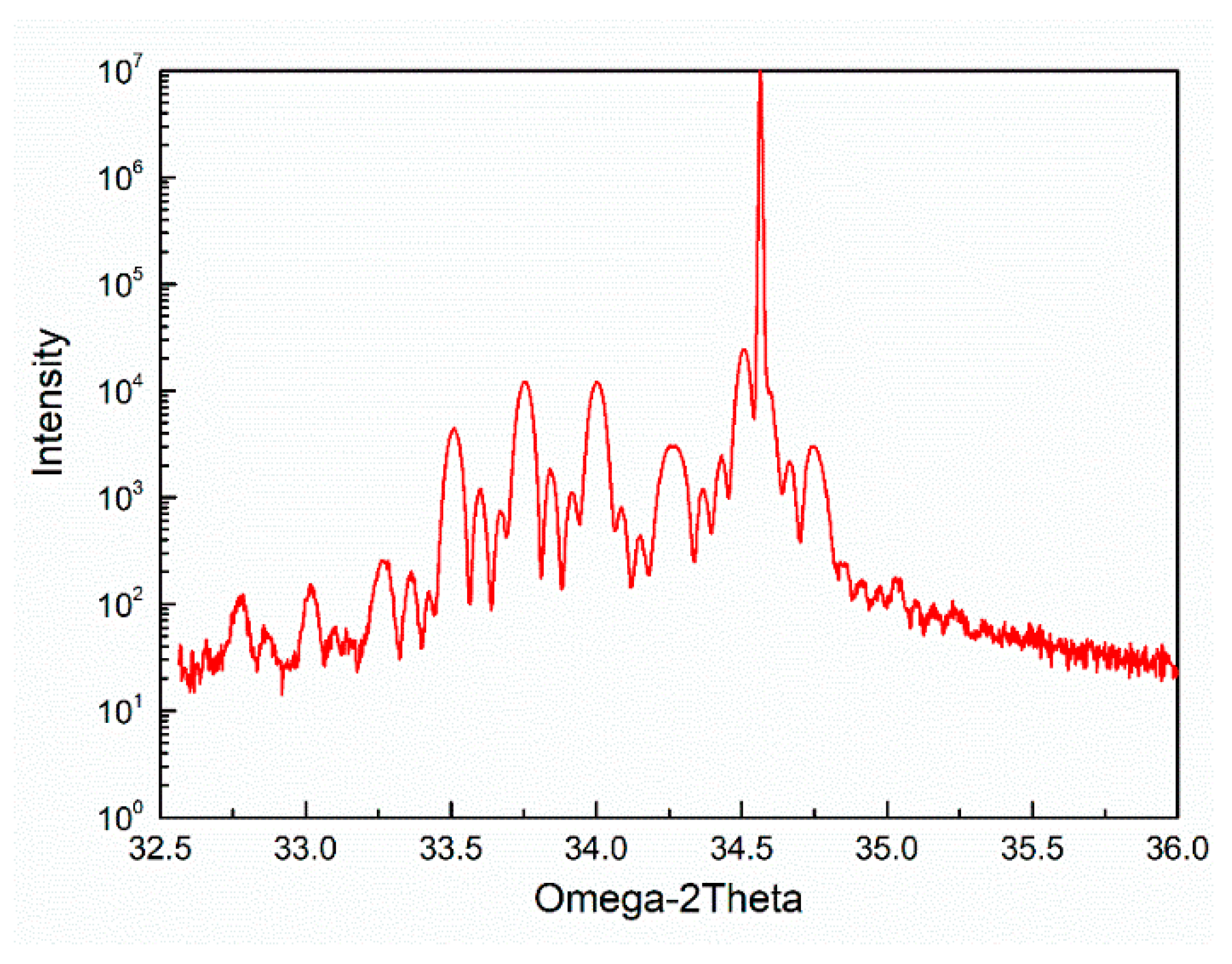
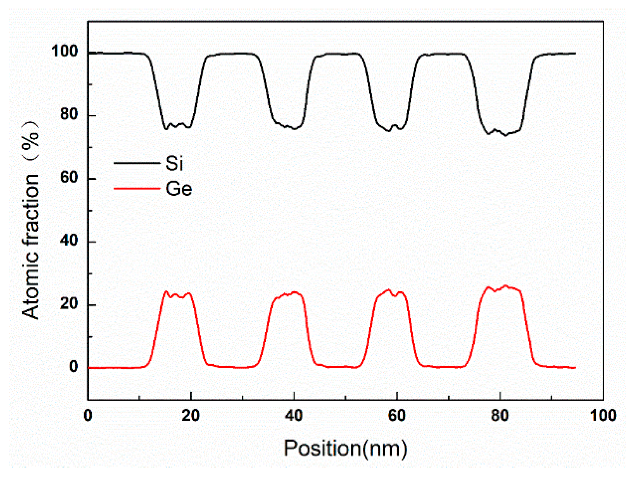
3.1. Epitaxial Growth of Stacked SiGe/Si Multilayer

After a standard HF-last clean, to maintain the well doping profile and attain an excellent surface of the Si substrate, a H2 pre-bake treatment of 825 °C for 5 min is performed. The epitaxial growth of stacked SiGe/Si multilayer is prepared using dichlorosilane (DCS) and GeH4 as SiGe layer precursors and SiH4 as Si layer precursor at 650 °C in H2 ambient, respectively. And a four-period stacked SiGe/Si is fabricated successfully on the Si substrate by appropriately exchanging the sequences of introduced gases.
The crystalline microstructure of the four-period stacked SiGe/Si multilayer epitaxial grown on Si substrate is detected by high resolution X-ray diffraction (HRXRD, Bruker, Tel Aviv, Israel) in the vicinity of the (004) Bragg peak with a Cu peak radiation. Its ω − 2θ HRXRD scan result is shown in Figure 2. It is worth to note that a series of obvious high-intensity satellite peaks are found, indicating that the epitaxial layers of the four-period stacked SiGe/Si multilayer are under strained due to the lattice constant mismatch of Si and SiGe. Moreover, the presence of small-intensity thickness fringes is the characteristic of high quality of the stacked SiGe/Si multilayer.
In addition, its high-angle annular dark field scanning transmission electron microscopy (HAADF-STEM, FEI Talos, Brno, Czech Republic) analysis results are shown in Figure 3. It is found that there are no misfits at the SiGe/Si interfaces, nor threading dislocations crossing the stacked SiGe/Si epitaxial film. Therefore, a high crystal quality four-period stacked SiGe/Si multilayer with thin and distinct interfaces between SiGe and Si is successfully prepared. Meanwhile, the thickness of SiGe from top to bottom is 8.3, 8.2, 8.1 and 10.1 nm under the same time of epitaxial grown. Namely, the thickness of bottom SiGe is ~2 nm thicker than that of others. It is known that the epitaxial rate is strongly dependent on the crystallization of under-layer, that is, the epitaxial rate might be decreased if multi-crystallization occurs in the under-layer.
Subsequently, EDX (FEI Talos, Brno, Czech Republic) line scan analysis of Ge and Si elements is also performed to determine the interfacial morphologies, and atomic fraction of the SiGe/Si layers for the four-period stacked SiGe/Si multilayer. The result is shown in Figure 4. It can be observed that the Ge atomic fraction of the SiGe layers from top to bottom are 23.2%, 23.5%, 23.8%, and 24.5%, respectively. Moreover, the width of transition layer of Si and SiGe are within 1.5 nm. Therefore, very uniform Ge atomic fraction of the SiGe layers with sharp SiGe/Si interfaces are achieved.

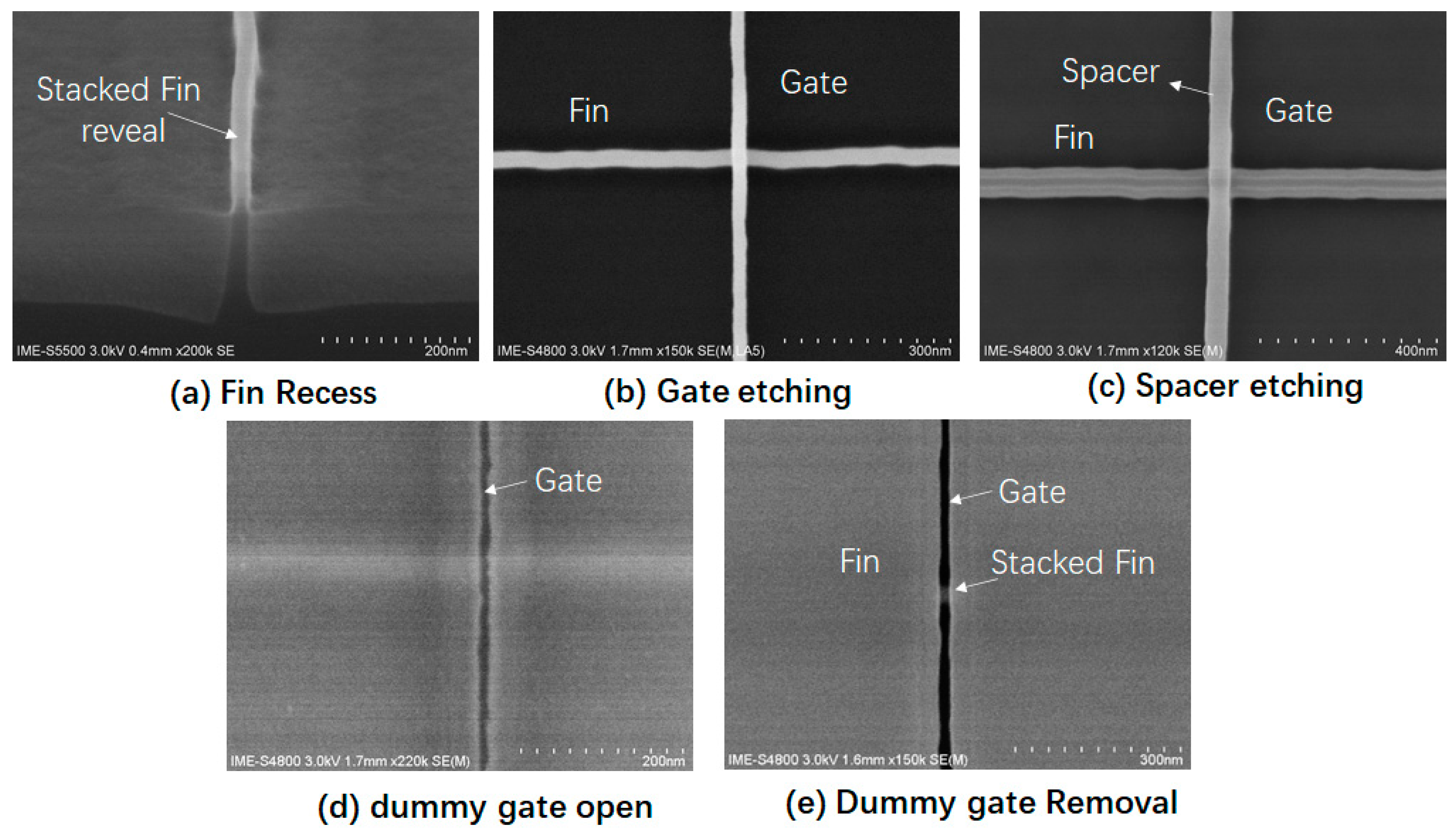
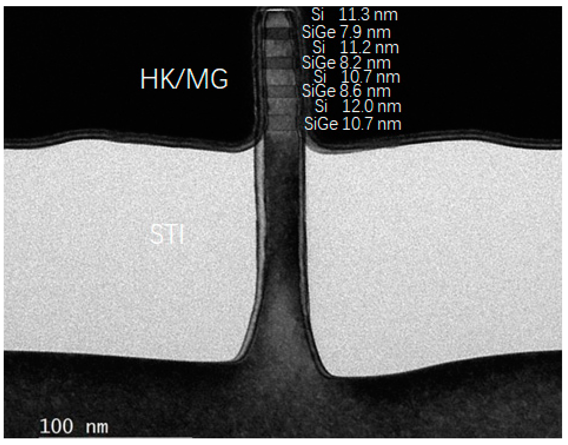
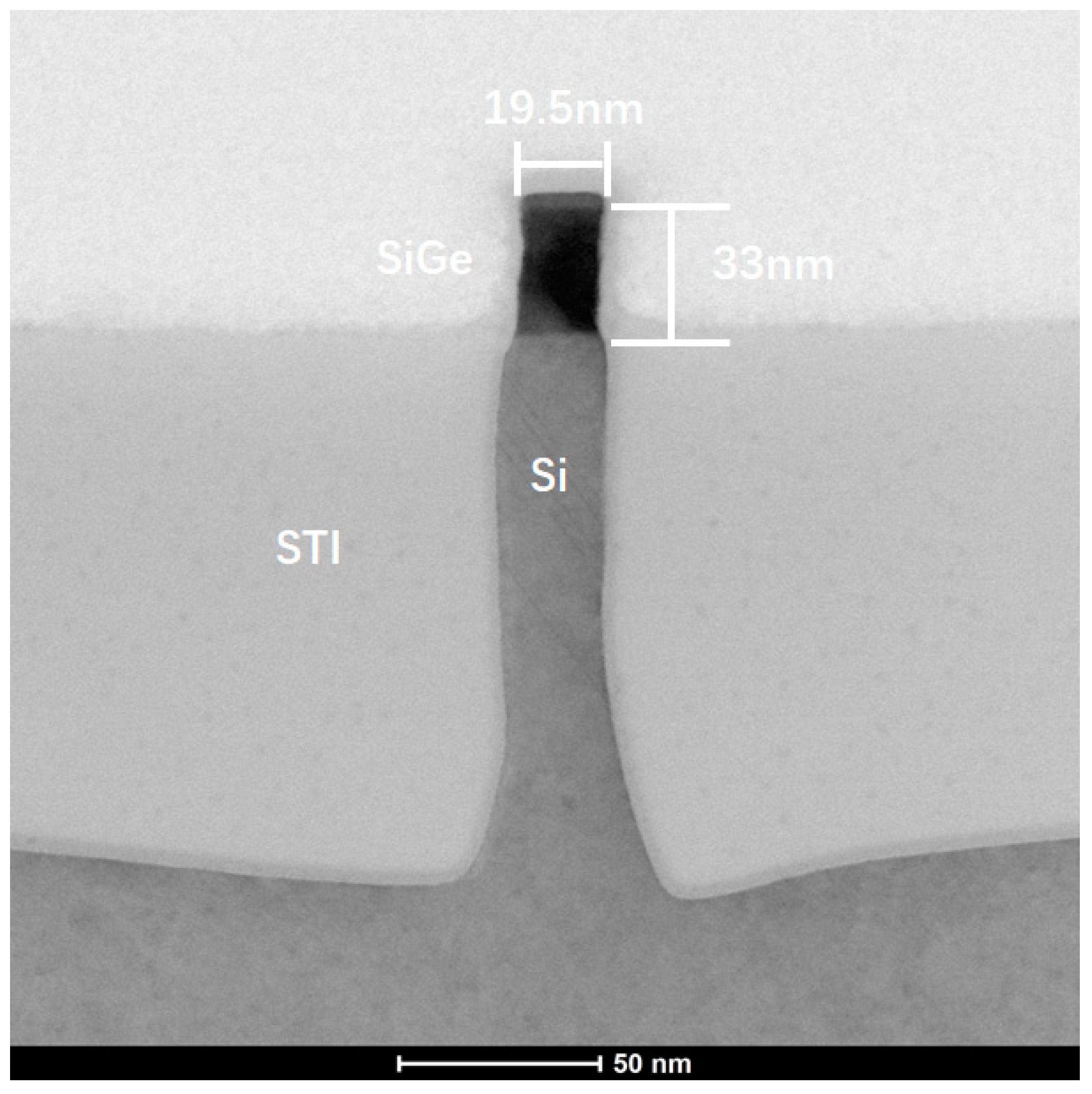
3.2. Stacked SiGe/Si Fin Etching

Based on previous SiGe Fin etching result, HBr-based plasma is chosen as the etching gas for the four-period stacked SiGe/Si multilayer. Figure 5 presents the profiles of Si substrate/four-period stacked SiGe/Si multilayer Fin produced by HBr/O2/He plasma under different bias voltage and O2 flow. The other etching process conditions are as follows: top power of 350 W, pressure of 6 mTorr, HBr flow of 110 sccm, He flow of 50 sccm. A more vertical profile of the Si substrate/four-period stacked SiGe/Si multilayer Fin structure can be achieved as its bias voltage increase from −70 V to −90 V and its O2 flow increasing from 2.2 to 2.5 sccm. This is because that increasing the bias voltage can attain a larger ion bombardment effect and slightly increasing O2 flow can help promote passivation films formation on the stacked SiGe/Si Fin sidewall and preserve its profile during etching.

3.3. FinFET Device Fabrication

After these above newly developed epitaxial growth and etching technologies are implemented, the results of following major fabrication process of the four-period stacked SiGe/Si channel FinFET device are shown in Figure 6. Figure 6a presents the cross-sectional SEM image of the Fin reveal structure post STI recess by 1:100 diluted HF solution. It is found that the STI is well controlled and the stacked SiGe/Si Fin on the top of the Si has been revealed. Figure 6b shows the top view SEM image of stacked SiGe/Si channel FinFET device after gate formation with critical dimension (CD) of ~25 nm. And conformal spacer 1 and spacer 2 in Figure 6c are realized at two sides of dummy gate. Figure 6d,e present a top view of stacked SiGe/Si channel FinFET device after dummy gate CMP and dummy gate removal. As can be seen from the images, the surface of ILD is very smooth, and a dummy poly gate is successfully removed with a stacked SiGe/Si channel exposure in the open gate trench. After dummy gate removal, an in-situ low temperature O3 passivation treatment at 300 °C for 1 min and the Al2O3/HfO2 and TiN/TaN/TiN//W are implemented as HK and MG, respectively. Figure 7 shows cross-sectional transmission electron microscopy (TEM) image for the four-period stacked SiGe/Si channel under the HK/MG stack at the end of fabrication processing. And its HAADF-STEM and EDS mapping results are shown in Figure 8. It is found that a perfect four-period stacked SiGe/Si channel Fin structure with stable SiGe and Si layers is realized and the multilayer HK/MG are well wrapped around. At the same time, the Fin height of SiGe channel is 80.6 nm and the CD is 20 nm.

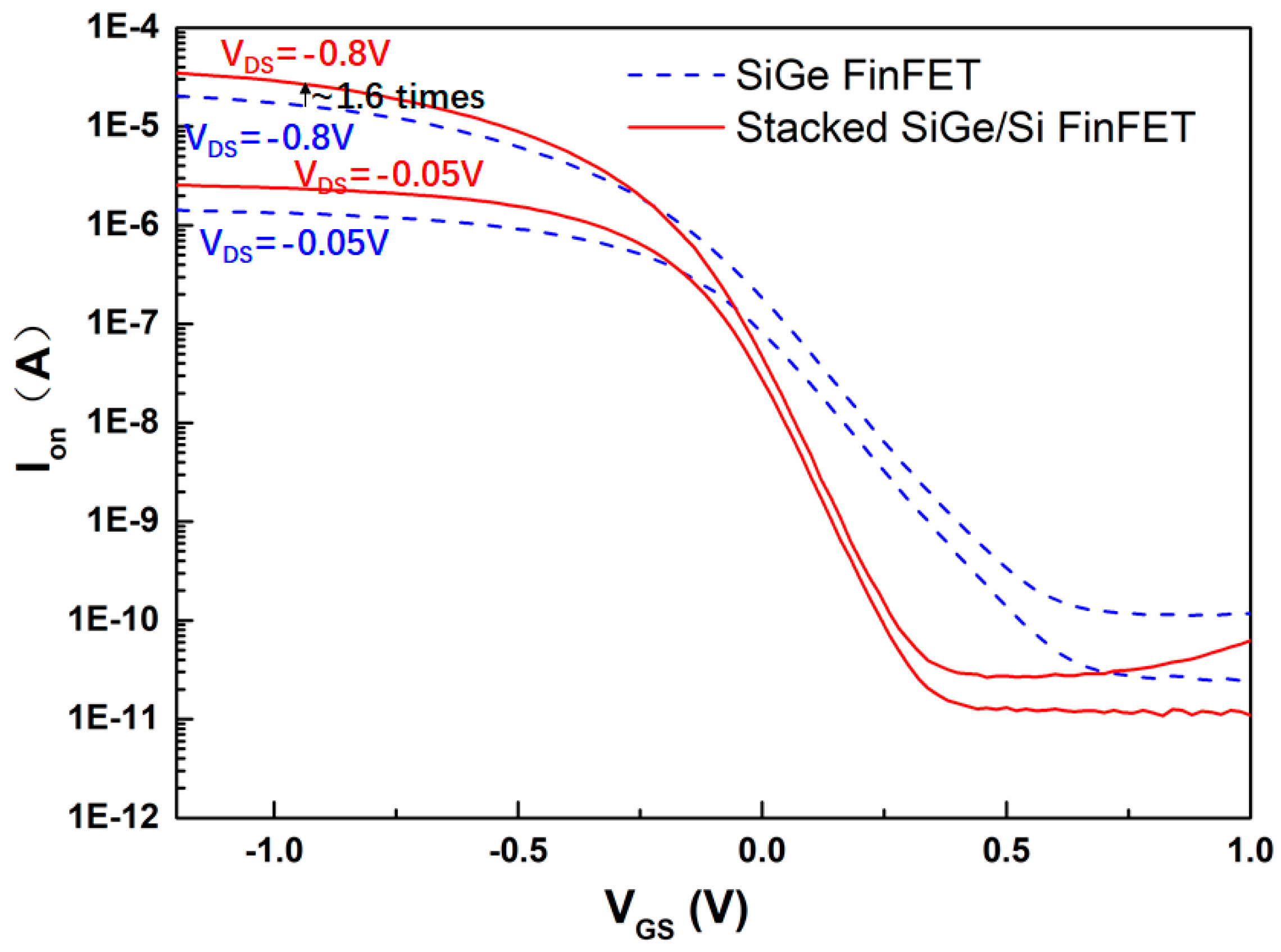
3.4. Electrical Performance

As a comparison, the conventional SiGe channel FinFET is also fabricated under the similar fabrication process.
As shown in Figure 9, the Fin height of its SiGe channel is 33 nm and the CD is 19.5 nm. The Fin height of SiGe channel is almost equal to total thickness of SiGe in the four-period stacked SiGe/Si channel FinFET. Moreover, the CD and profile of Fin of these two kinds of FinFET device are almost comparable. Therefore, these two kinds of FinFET device have almost the same footprint.
Figure 10 shows the IDS-VGS curves for the four-period stacked SiGe/Si channel FinFET and conventional SiGe channel FinFET. Compared with conventional SiGe channel FinFET, the Ion, SS and Ion/Ioff ratio of the four-period stacked SiGe/Si channel FinFET under the same footprint show obvious benefit. And their electrical characteristic data are summarized in Table 1. Its Ion under VDS = VGS = −0.8 V increases 1.6 times, improved from 13.3 µA to 21.2 µA, and its Ion/Ioff ratio can be improved from 1 × 10⁵ to 1 × 10⁶ due to the increase of Ion and the decrease of Ioff at the same time. At the same time, the threshold voltage (Vtsat) extracting at Ion of 1 × 10⁻⁹ A can be improved from +0.38 V to +0.16 V. In addition, four-period stacked SiGe/Si channel FinFET is easier to obtain a better SS characteristic than the conventional SiGe FinFET under the same unoptimized O3 passivation process. Its SS can be improved from 149 mV/dec to 90 mV/dec. The better SS characteristic should be related to the four-period stacked SiGe/Si Fin structure and it also can help to increase the Ion and decrease the Ioff. The better SS can be attributed to the following two reasons: first, the stacked SiGe/Si with each layer SiGe of 8–10 nm in the stable stage may maintain a better quality and surface interfacial performance during the whole fabrication process compared with the the conventional SiGe of 33 nm in the metastable stage; second, the Si channel of the stacked SiGe/Si channel may turn on first due to its lower Dit. Moreover, the larger Ion can be attributed to the increasing of effective channel width (Weff) because the Weff of four-period stacked SiGe/Si Fin is 181 nm and the Weff of conventional SiGe Fin is only 85.5 nm.
This four-period stacked SiGe/Si channel FinFET has been demonstrated to be a practical candidate for the future technology nodes. However, it is important to emphasize that these results are preliminary for the four-period stacked SiGe/Si channel FinFET, and there is still much room to improve its electrical characteristic, such as its SS and Vtsat. Therefore, we will employ the interfacial passivation, and gate stack engineering to further optimize its electrical performance in the future.

4. Conclusions

In a summary, a four-period vertically stacked SiGe/Si FinFET device was successfully fabricated by optimizing its epitaxial grown and Fin etching process. Compared with the conventional SiGe channel FinFET under the same footprint, its Ion increases 1.6 times, Ion/Ioff ratio increases 1 order and SS can be improved from 149 to 90 mV/dec because the four-period stacked SiGe/Si Fin structure has larger Weff and may maintain a better quality and surface interfacial performance during the whole fabrication process. Therefore, this device has been demonstrated to be a practical candidate for future technology nodes. Moreover, considering the compatibility of fabrication process, it also can be use as the I/O device for the vertically stacked Gate-All-Around horizontal nanowire/sheet technology if a thicker gate stack is employed and the channel release step is skipped.

Author Contributions

Methodology, Y.L., F.Z. and X.C.; investigation, Y.L., F.Z., H.L. and Y.Z.; data curation, Y.L., X.C., J.L. (Junjie Li) and Q.Z.; writing—original draft preparation, Y.L., F.Z., X.C., Z.W. and J.L. (Jun Luo); writing—review and editing, Y.L., F.Z. and X.C.; project administration, Y.L.; funding acquisition, Y.L. and W.W. All authors have read and agreed to the published version of the manuscript.

Funding

This work is supported in part by National Natural Science Foundation of China (Grant no. 62074160), in part by the Science and Technology Program of Beijing Municipal Science and Technology Commission (grant no. Z201100004220001), in part by the CAS Pioneer Hundred Talents Program, in part by Beijing Municipal Natural Science Foundation (Grant no. 4202078), and in part by the National Key Project of Science and Technology of China (Grant no. 2017ZX02315001-002).

Institutional Review Board Statement

Not applicable.

Informed Consent Statement

Not applicable.

Data Availability Statement

Not applicable.

Acknowledgments

We thank the Integrated Circuit Advanced Process Center (ICAC) at the Institute of Microelectronics of the Chinese Academy of Sciences for the devices fabricated on their advanced 200 mm CMOS platform.

Conflicts of Interest

The authors declare no conflict of interest.

References

  1. Yeap, G.; Lin, S.S.; Chen, Y.M.; Shang, H.L.; Wang, P.W.; Lin, H.C.; Peng, Y.C.; Sheu, J.Y.; Wang, M.; Chen, X.; et al. 5 nm CMOS Production Technology Platform featuring full-fledged EUV, and High Mobility Channel FinFETs with densest 0.021 µm2 SRAM cells for Mobile SoC and High Performance Computing Applications. In Proceedings of the 2019 IEEE International Electron Devices Meeting (IEDM), San Francisco, CA, USA, 7–11 December 2019; pp. 36.7.1–36.7.4. [Google Scholar]
  2. Mertens, H.; Ritzenthaler, R.; Arimura, H.; Franco, J.; Sebaai, F.; Hikavyy, A.; Pawlak, B.; Machkaoutsan, V.; Devriendt, K.; Tsvetanova, D. Si-cap-free SiGe p-channel FinFETs and gate-all-around transistors in a replacement metal gate process: Interface trap density reduction and performance improvement by high-pressure deuterium anneal. In Proceedings of the 2015 Symposium on VLSI Technology (VLSI Technology), Kyoto, Japan, 16–18 June 2015; pp. T142–T143. [Google Scholar]
  3. Witters, L.; Arimura, H.; Sebaai, F.; Hikavyy, A.; Milenin, A.P.; Loo, R.; De Keersgieter, A.; Eneman, G.; Schram, T.; Wostyn, K.; et al. Strained Germanium Gate-All-Around pMOS Device Demonstration Using Selective Wire Release Etch Prior to Replacement Metal Gate Deposition. IEEE Trans. Electron Devices 2017, 64, 4587–4593. [Google Scholar] [CrossRef]
  4. Franco, J.; Kaczer, B.; Roussel, P.J.; Mitard, J.; Cho, M.; Witters, L.; Grasser, T.; Groeseneken, G. SiGe Channel Technology: Superior Reliability Toward Ultrathin EOT Devices-Part I: NBTI. IEEE Trans. Electron Devices 2013, 60, 396–404. [Google Scholar] [CrossRef]
  5. Lee, C.H.; Southwick, R.G.; Mochizuki, S.; Li, J.; Miao, X.; Wang, M.; Bao, R.; Ok, I.; Ando, T.; Hashemi, P.; et al. Toward High Performance SiGe Channel CMOS: Design of High Electron Mobility in SiGe nFinFETs Outperforming Si. In Proceedings of the 2018 IEEE International Electron Devices Meeting (IEDM), San Francisco, CA, USA, 1–5 December 2018; pp. 35.1.1–35.1.4. [Google Scholar]
  6. Zhao, Z.Q.; Li, Y.; Zan, Y.; Li, Y.L.; Li, J.J.; Cheng, X.H.; Wang, G.L.; Liu, H.Y.; Wang, H.X.; Zhang, Q.Z.; et al. Fabrication technique of the Si0.5Ge0.5 Fin for the high mobility channel FinFET device. Semicond. Sci. Technol. 2020, 35, 045015. [Google Scholar] [CrossRef]
  7. Zhao, Z.Q.; Li, Y.L.; Wang, G.L.; Du, A.Y.; Li, Y.; Zhang, Q.Z.; Xu, G.B.; Zhang, Y.K.; Luo, J.; Li, J.F.; et al. Process optimization of the Si0.7Ge0.3 Fin Formation for the STI first scheme. Semicond. Sci. Technol. 2019, 34, 125008. [Google Scholar] [CrossRef]
  8. Mochizuki, S.; Colombeau, B.; Zhang, J.; Kung, S.C.; Stolfi, M.; Zhou, H.; Breton, M.; Watanabe, K.; Li, J.; Jagannathan, H.; et al. Structural and Electrical Demonstration of SiGe Cladded Channel for PMOS Stacked Nanosheet Gate-All-Around Devices. In Proceedings of the 2020 IEEE Symposium on VLSI Technology, Honolulu, HI, USA, 16–19 June 2020; pp. 1–2. [Google Scholar]
  9. Paul, D.J. Si/SiGe heterostructures: From material and physics to devices and circuits. Semicond. Sci. Technol. 2004, 19, R75–R108. [Google Scholar] [CrossRef]
  10. Arimura, H.; Wostyn, K.; Ragnarsson, L.Å.; Capogreco, E.; Chasin, A.; Conard, T.; Brus, S.; Favia, P.; Franco, J.; Mitard, J.; et al. Ge oxide scavenging and gate stack nitridation for strained Si0.7Ge0.3 pFinFETs enabling 35% higher mobility than Si. In Proceedings of the 2019 IEEE International Electron Devices Meeting (IEDM), San Francisco, CA, USA, 7–11 December 2019; pp. 29.2.1–29.2.4. [Google Scholar]
  11. Jungwoo, O.; Majhi, P.; Jammy, R.; Joe, R.; Dip, A.; Takuya, S.; Yasushi, A.; Takanobu, K.; Tsunetoshi, A.; Masayuki, T. Additive mobility enhancement and off-state current reduction in SiGe channel pMOSFETs with optimized Si Cap and high-k metal gate stacks. In Proceedings of the 2009 International Symposium on VLSI Technology, Systems, and Applications, Hsinchu, Taiwan, 27–29 April 2009; pp. 22–23. [Google Scholar]
  12. Zhang, B.; Yu, W.; Zhao, Q.T.; Hartmann, J.; Lupták, R.; Buca, D.; Bourdelle, K.; Wang, X.; Mantl, S. High mobility Si/Si0.5Ge0.5/strained SOI p-MOSFET with HfO2 /TiN gate stack. In Proceedings of the 2010 10th IEEE International Conference on Solid-State and Integrated Circuit Technology, Shanghai, China, 1–4 November 2010; pp. 911–913. [Google Scholar]
  13. Ando, T.; Hashemi, P.; Bruley, J.; Rozen, J.; Ogawa, Y.; Koswatta, S.; Chan, K.K.; Cartier, E.A.; Mo, R.; Narayanan, V. High Mobility High-Ge-Content SiGe PMOSFETs Using Al2O3/HfO2 Stacks With In-Situ O3 Treatment. IEEE Electron Device Lett. 2017, 38, 303–305. [Google Scholar] [CrossRef]
  14. Lee, C.H.; Kim, H.; Jamison, P.; Southwick, R.G.; Mochizuki, S.; Watanabe, K.; Bao, R.; Galatage, R.; Guillaumet, S.; Ando, T.; et al. Selective GeOx-scavenging from interfacial layer on Si1−xGex channel for high mobility Si/Si1−xGex CMOS application. In Proceedings of the 2016 IEEE Symposium on VLSI Technology, Honolulu, HI, USA, 14–16 June 2016; pp. 1–2. [Google Scholar]
  15. Chang, K.M.; Chen, C.F.; Lai, C.H.; Kuo, P.S.; Chen, Y.M.; Chang, T.Y. Electrical properties of SiGe nanowire following fluorine/nitrogen plasma treatment. Appl. Surf. Sci. 2014, 289, 581–585. [Google Scholar] [CrossRef]
  16. Li, Y.; Cheng, X.; Zhong, Z.; Zhang, Q.; Wang, G.; Li, Y.; Li, J.; Ma, X.; Wang, X.; Yang, H.; et al. Key Process Technologies for Stacked Double Si0.7Ge0.3 Channel Nanowires Fabrication. ECS J. Solid State Sci. Technol. 2020, 9, 064009. [Google Scholar] [CrossRef]
Figure 1. Fabrication flow of four-period stacked SiGe/Si Channel FinFET device.
Nanomaterials 11 01689 g001
Figure 2. HRXRD spectra result on the four-period stacked SiGe/Si multilayer epitaxial grown on Si substrate.
Nanomaterials 11 01689 g002
Figure 3. (a)Cross-section HAADF-STEM images of four-period stacked SiGe/Si multilayer; (b) its magnified images at the SiGe/Si interfaces.
Nanomaterials 11 01689 g003
Figure 4. EDX line scan analysis of Ge and Si elements across the four-period stacked SiGe/Si multilayer.
Nanomaterials 11 01689 g004
Figure 5. Scanning electron microscope (SEM) images of Fin profile under HBr/O2/He plasma under (a) bias voltage of −70 V and O2 flow of 2.2 sccm, (b) bias voltage of −90 V and O2 flow of 2.5 sccm.
Nanomaterials 11 01689 g005
Figure 6. SEM images of stacked SiGe/Si channel FinFET device at different fabrication stages: (a) Fin reveal post STI recess, (b) dummy gate formation, (c) spacer formation, (d) poly gate open by CMP, (e) dummy gate removal.
Nanomaterials 11 01689 g006
Figure 7. TEM result of four-period stacked SiGe/Si channel FinFET under the HK/MG stack at the end of fabrication processing.
Nanomaterials 11 01689 g007
Figure 8. HAADF-STEM and EDS mapping results of the four-period stacked SiGe/Si channel FinFET under the HK/MG stack at the end of processing.
Nanomaterials 11 01689 g008
Figure 9. TEM result of the conventional SiGe channel Fin profile.
Nanomaterials 11 01689 g009
Figure 10. IDS-VGS characteristics of the four-period stacked SiGe/Si channel FinFET and conventional SiGe channel FinFET under the similar fabrication process.
Nanomaterials 11 01689 g010
Table 1. Electrical characteristic comparison of the four-period stacked SiGe/Si and conventional SiGe channel FinFET.
CategoryIon (µA)SS (mV/dec)Vtsat (V)Ion/Ioff
Conventional SiGe channel FinFET13.31490.381 × 105
Four-period stacked SiGe/Si channel FinFET21.2900.161 × 106
Publisher’s Note: MDPI stays neutral with regard to jurisdictional claims in published maps and institutional affiliations.

