
Core-Shell Dual-Gate Nanowire Charge-Trap Memory for Synaptic Operations for Neuromorphic Applications


Abstract
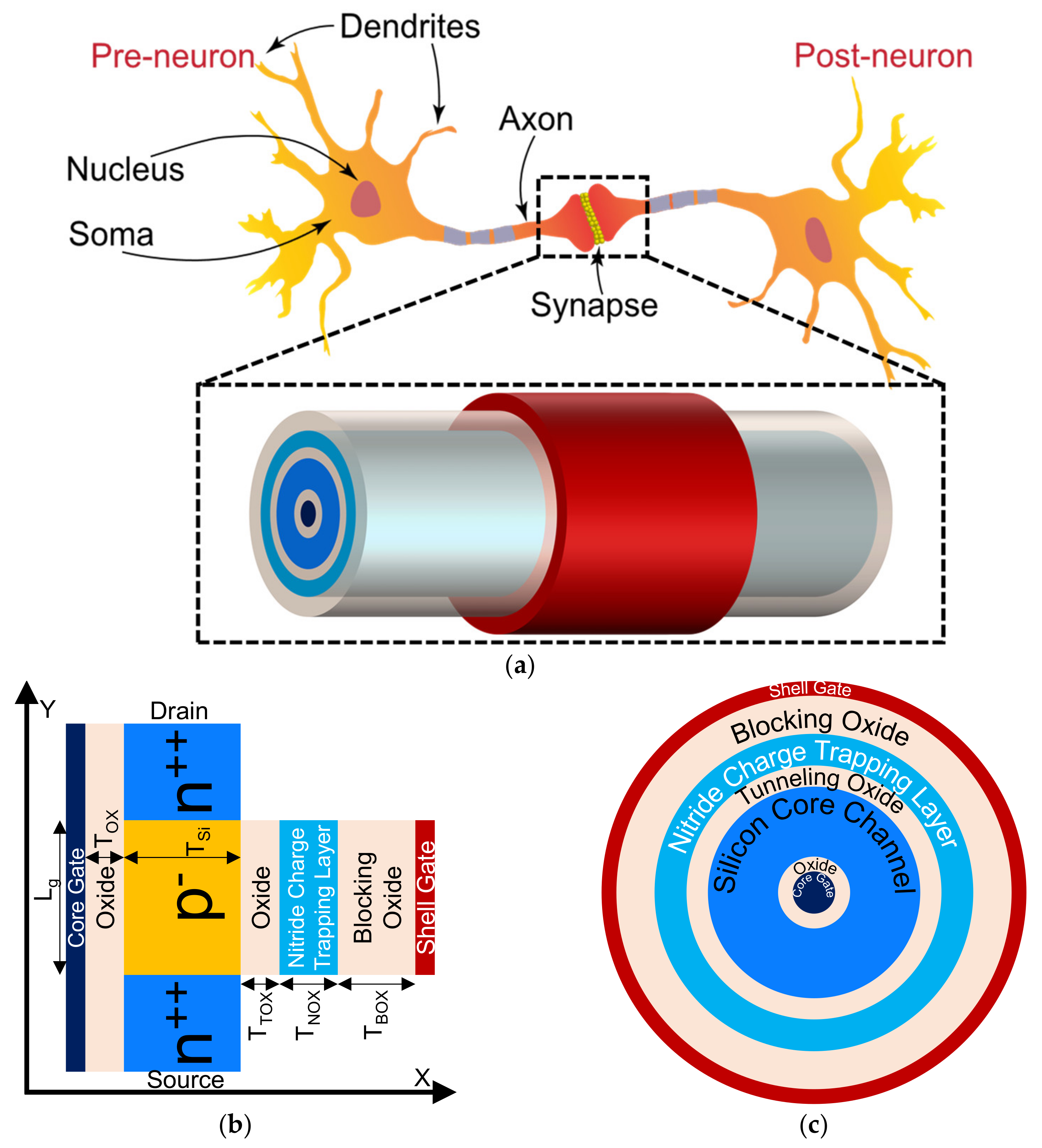
:1. Introduction
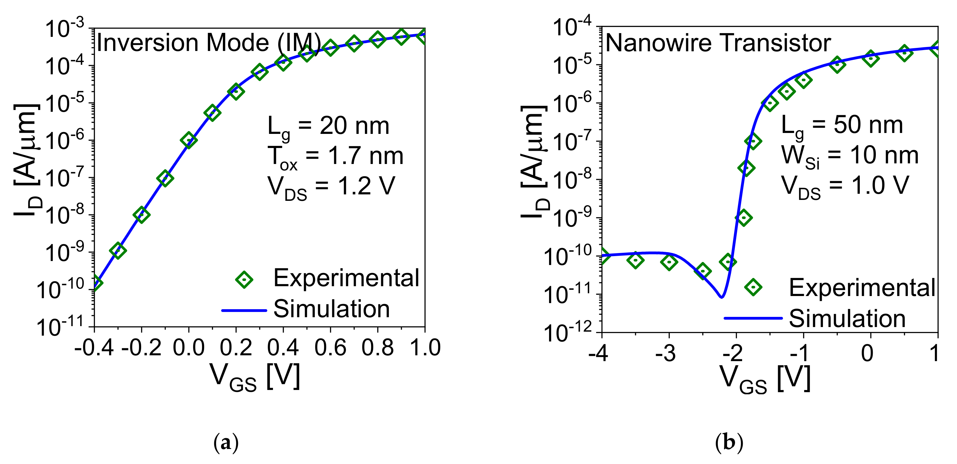
2. Device Design Strategies and Models Calibration
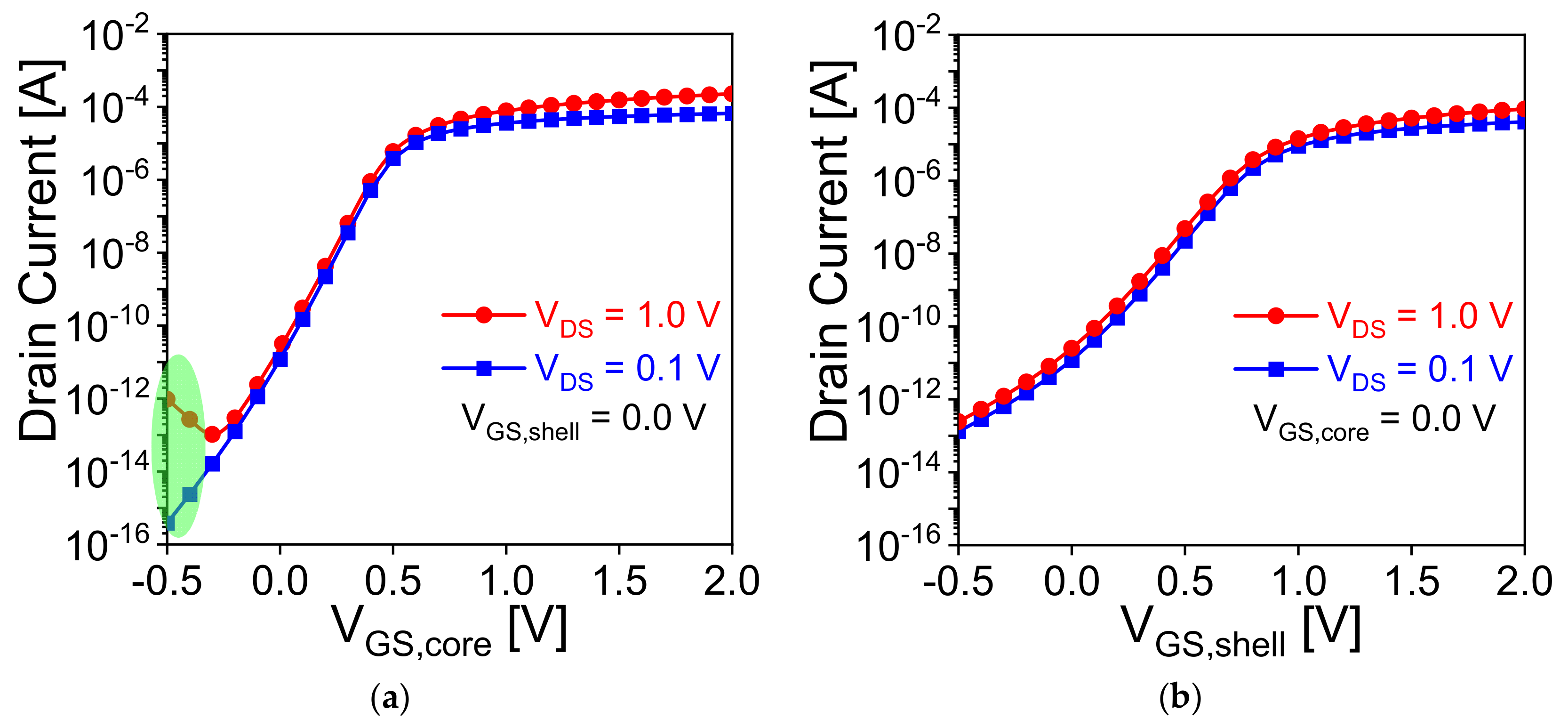
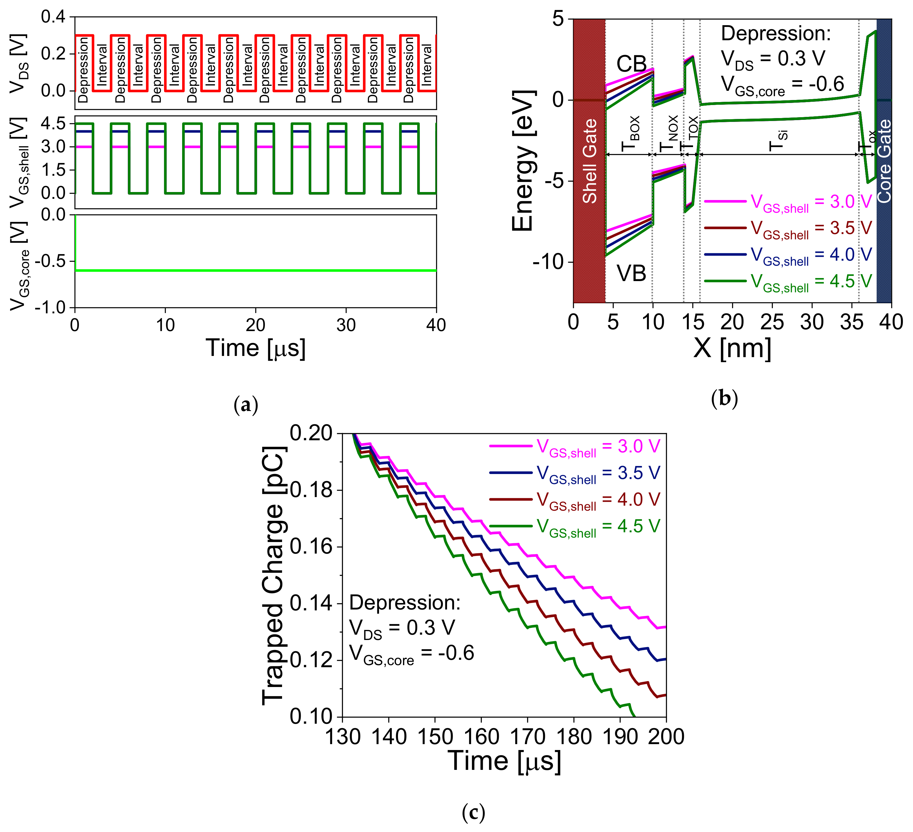
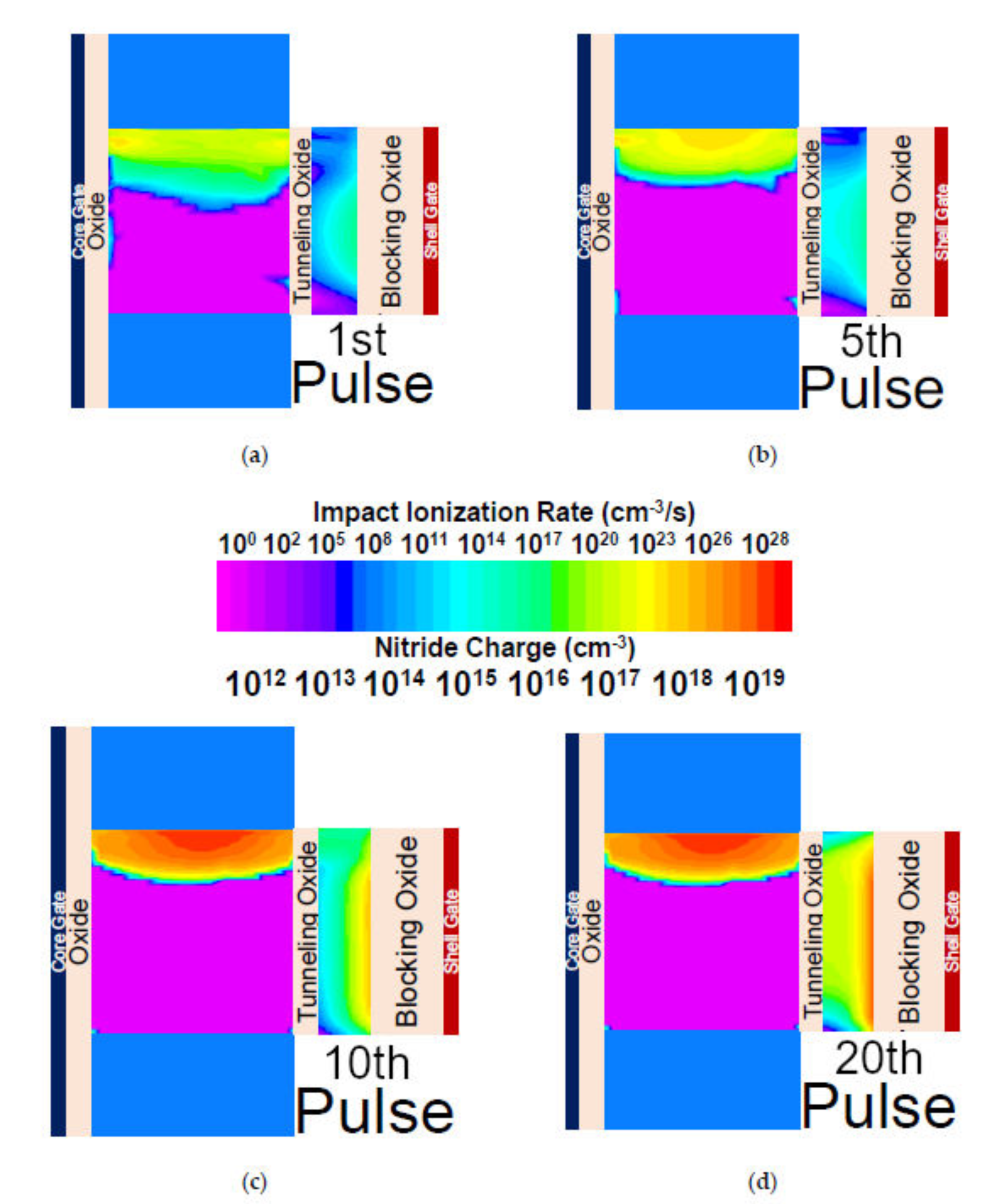
3. Results and Discussion
4. Conclusions
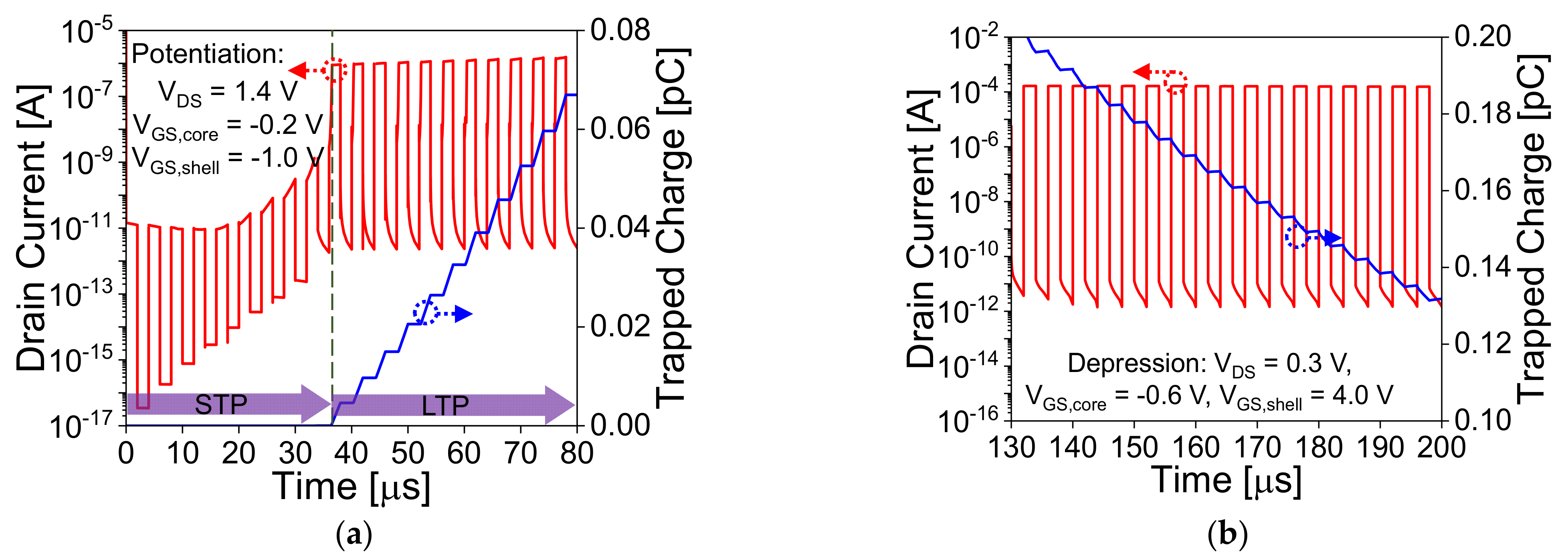
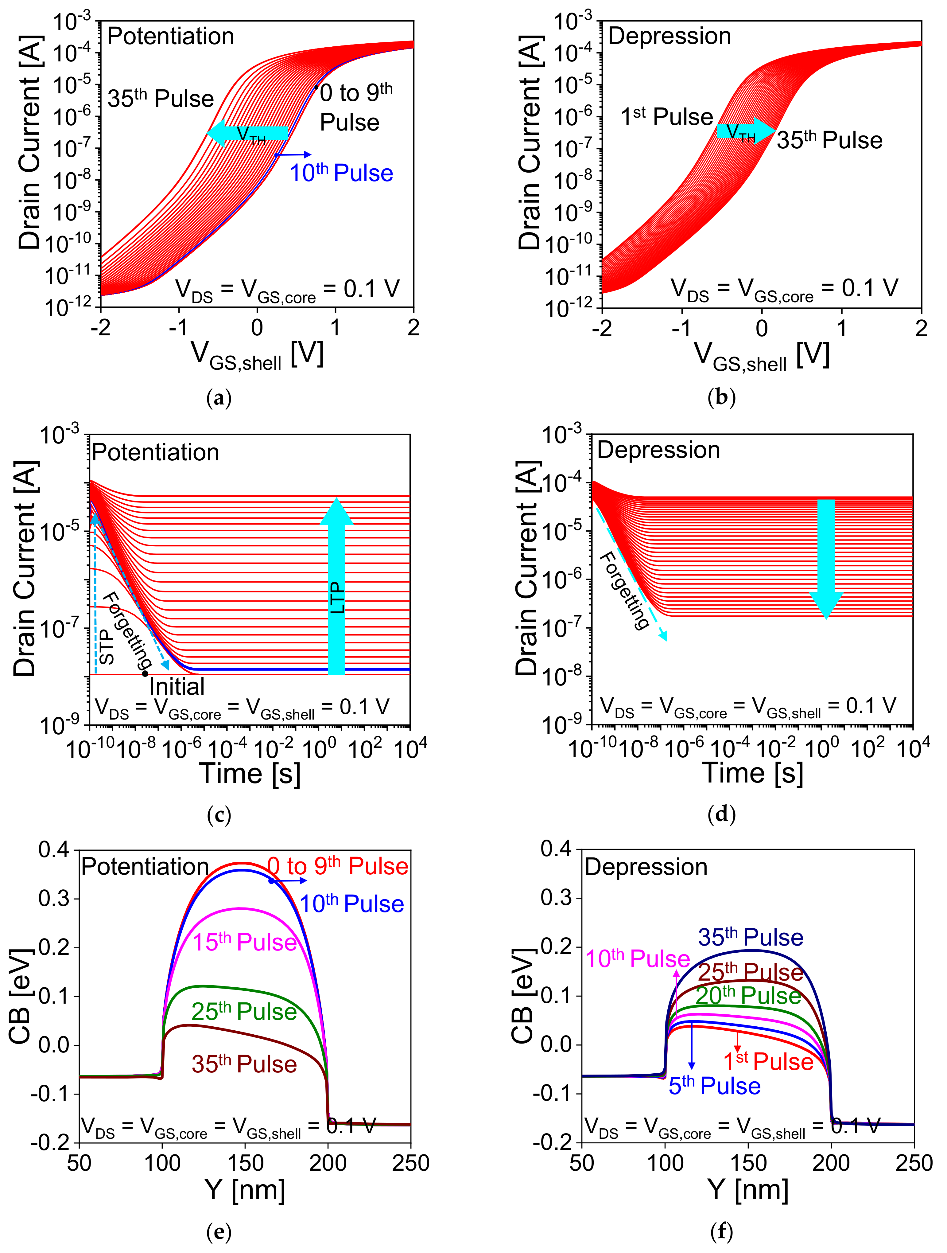
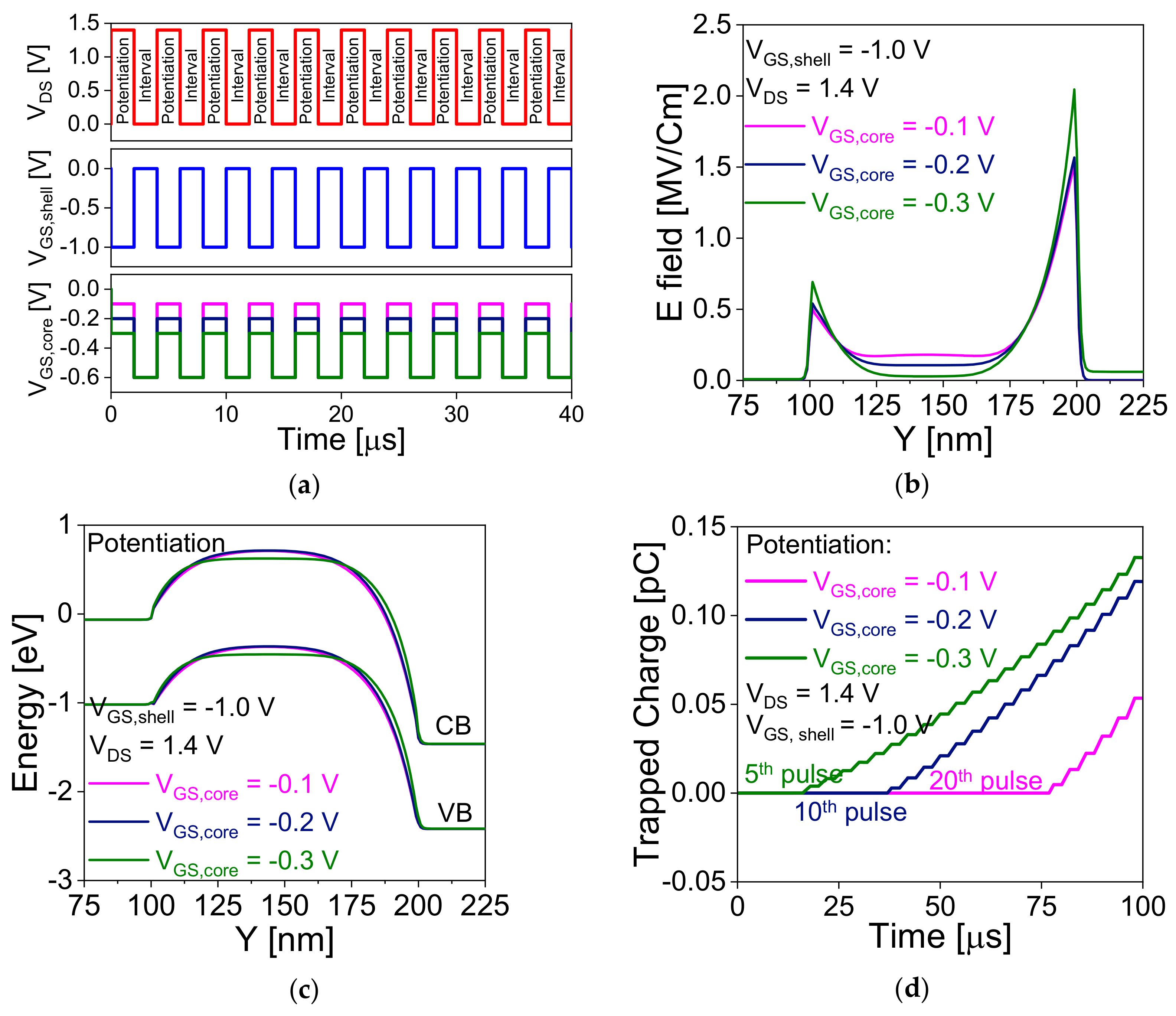
- Transformation from STP to LTP occurs at the 10th pulse and it can be modulated through core gate voltage (VGS,core) because the tunneling is governed through VGS,core.
- The trade-off between change in threshold voltage, and linearity in, conductance is observed during depression operation.
- We can investigate the learning and inference capabilities of the proposed synaptic device for hardware based neural networks (HNN).
- A reliable and consistent digit recognition accuracy of 92.28% is achieved by a single layer neural network on the MNIST dataset.
Author Contributions
Funding
Data Availability Statement
Conflicts of Interest
References
- Kuzum, D.; Yu, S.; Philip Wong, H.-S. Synaptic electronics: Materials, devices and applications. Nanotechnology 2013, 24, 38200. [Google Scholar] [CrossRef] [PubMed]
- Indiveri, G.; Liu, S.-C. Memory and Information Processing in Neuromorphic Systems. Proc. IEEE 2015, 103, 1379–1397. [Google Scholar] [CrossRef] [Green Version]
- Kim, S.; Yoon, J.; Kim, H.-D.; Choi, S.-J. Carbon Nanotube Synaptic Transistor Network for Pattern Recognition. ACS Appl. Mater. Interfaces 2015, 7, 25479–25486. [Google Scholar] [CrossRef] [PubMed]
- Tang, B.; Hussain, S.; Xu, R.; Cheng, Z.; Liao, J.; Chen, Q. Novel Type of Synaptic Transistors Based on a Ferroelectric Semiconductor Channel. ACS Appl. Mater. Interfaces 2020, 12, 24920–24928. [Google Scholar] [CrossRef]
- Ambrogio, S.; Ciocchini, N.; Laudato, M.; Milo, V.; Pirovano, A.; Fantini, P.; Ielmini, D. Unsupervised Learning by Spike Timing Dependent Plasticity in Phase Change Memory (PCM) Synapses. Front. Neurosci. 2016, 10, 1–12. [Google Scholar] [CrossRef] [PubMed] [Green Version]
- Burr, G.W.; Shelby, R.M.; Sebastian, A.; Kim, S.; Kim, S.; Sidler, S.; Virwani, K.; Ishii, M.; Narayanan, P.; Fumarola, A.; et al. Neuromorphic computing using non-volatile memory. Adv. Phys. X 2017, 2, 89–124. [Google Scholar] [CrossRef]
- Kang, D.; Jang, J.T.; Park, S.; Ansari, M.H.R.; Bae, J.-H.; Choi, S.-J.; Kim, D.M.; Kim, C.; Cho, S.; Kim, D.H. Threshold-Variation-Tolerant Coupling-Gate α-IGZO Synaptic Transistor for More Reliably Controllable Hardware Neuromorphic System. IEEE Access 2021, 9, 59345–59352. [Google Scholar] [CrossRef]
- Sun, B.; Guo, T.; Zhou, G.; Ranjan, S.; Jiao, Y.; Wei, L.; Zhou, Y.N.; Wu, Y.A. Synaptic devices based neuromorphic computing applications in artificial intelligence. Mater. Today Phys. 2021, 18, 100393. [Google Scholar] [CrossRef]
- Ryu, J.-H.; Kim, B.; Hussain, F.; Ismail, M.; Mahata, C.; Oh, T.; Imran, M.; Min, K.K.; Kim, T.-H.; Yang, B.-D.; et al. Zinc Tin Oxide Synaptic Device for Neuromorphic Engineering. IEEE Access 2020, 8, 130678–130686. [Google Scholar] [CrossRef]
- Lee, D.K.; Kim, M.-H.; Bang, S.; Kim, T.-H.; Choi, Y.-J.; Kim, S.; Cho, S.; Park, B.-G. HfOx-based nano-wedge structured resistive switching memory device operating at sub- μ A current for neuromorphic computing application. Semicond. Sci. Technol. 2020, 35, 055002. [Google Scholar] [CrossRef]
- Kim, M.-H.; Cho, S.; Park, B.-G. Nanoscale wedge resistive-switching synaptic device and experimental verification of vector-matrix multiplication for hardware neuromorphic application. Jpn. J. Appl. Phys. 2021, 60, 050905. [Google Scholar] [CrossRef]
- Cho, S.W.; Kwon, S.M.; Kim, Y.-H.; Park, S.K. Recent Progress in Transistor-Based Optoelectronic Synapses: From Neuromorphic Computing to Artificial Sensory System. Adv. Intell. Syst. 2021, 2000162, 2000162. [Google Scholar] [CrossRef]
- Sun, B.; Ranjan, S.; Zhou, G.; Guo, T.; Du, C.; Wei, L.; Zhou, Y.N.; Wu, Y.A. A True Random Number Generator Based on Ionic Liquid Modulated Memristors. ACS Appl. Electron. Mater. 2021, 3, 2380–2388. [Google Scholar] [CrossRef]
- Kim, D.; Jang, J.T.; Yu, E.; Park, J.; Min, J.; Kim, D.M.; Choi, S.J.; Mo, H.S.; Cho, S.; Roy, K.; et al. Pd/IGZO/p+-Si Synaptic Device with Self-Graded Oxygen Concentrations for Highly Linear Weight Adjustability and Improved Energy Efficiency. ACS Appl. Electron. Mater. 2020, 2, 2390–2397. [Google Scholar] [CrossRef]
- Kim, H.; Hwang, S.; Park, J.; Park, B.G. Silicon synaptic transistor for hardware-based spiking neural network and neuromorphic system. Nanotechnology 2017, 28. [Google Scholar] [CrossRef] [PubMed]
- Yu, E.; Cho, S.; Park, B.-G. A Silicon-Compatible Synaptic Transistor Capable of Multiple Synaptic Weights toward Energy-Efficient Neuromorphic Systems. Electronics 2019, 8, 1102. [Google Scholar] [CrossRef] [Green Version]
- Kim, H.; Park, J.; Kwon, M.-W.; Lee, J.-H.; Park, B.-G. Silicon-Based Floating-Body Synaptic Transistor With Frequency-Dependent Short- and Long-Term Memories. IEEE Electron Device Lett. 2016, 37, 249–252. [Google Scholar] [CrossRef]
- Yu, R.; Li, E.; Wu, X.; Yan, Y.; He, W.; He, L.; Chen, J.; Chen, H.; Guo, T. Electret-Based Organic Synaptic Transistor for Neuromorphic Computing. ACS Appl. Mater. Interfaces 2020, 12, 15446–15455. [Google Scholar] [CrossRef]
- Yu, E.; Cho, S.; Roy, K.; Park, B.G. A Quantum-Well Charge-Trap Synaptic Transistor with Highly Linear Weight Tunability. IEEE J. Electron Devices Soc. 2020, 8, 834–840. [Google Scholar] [CrossRef]
- Seo, Y.-T.; Lee, M.-S.; Kim, C.-H.; Woo, S.Y.; Bae, J.-H.; Park, B.-G.; Lee, J.-H. Si-Based FET-Type Synaptic Device with Short-Term and Long-Term Plasticity Using High-κ Gate-Stack. IEEE Trans. Electron Devices 2019, 66, 917–923. [Google Scholar] [CrossRef]
- Moon, K.; Lim, S.; Park, J.; Sung, C.; Oh, S.; Woo, J.; Lee, J.; Hwang, H. RRAM-based synapse devices for neuromorphic systems. Faraday Discuss. 2019, 213, 421–451. [Google Scholar] [CrossRef]
- Ielmini, D. Brain-inspired computing with resistive switching memory (RRAM): Devices, synapses and neural networks. Microelectron. Eng. 2018, 190, 44–53. [Google Scholar] [CrossRef]
- Ferain, I.; Colinge, C.A.; Colinge, J.P. Multigate transistors as the future of classical metal-oxide-semiconductor field-effect transistors. Nature 2011, 479, 310–316. [Google Scholar] [CrossRef] [PubMed]
- Fahad, H.M.; Smith, C.E.; Rojas, J.P.; Hussain, M.M. Silicon Nanotube Field Effect Transistor with Core–Shell Gate Stacks for Enhanced High-Performance Operation and Area Scaling Benefits. Nano Lett. 2011, 11, 4393–4399. [Google Scholar] [CrossRef] [PubMed]
- Fahad, H.M.; Hussain, M.M. Are Nanotube Architectures More Advantageous Than Nanowire Architectures For Field Effect Transistors? Sci. Rep. 2012, 2, 475. [Google Scholar] [CrossRef] [PubMed] [Green Version]
- Sahay, S.; Kumar, M.J. Nanotube Junctionless FET: Proposal, Design, and Investigation. IEEE Trans. Electron Devices 2017, 64, 1851–1856. [Google Scholar] [CrossRef]
- Tekleab, D. Device Performance of Silicon Nanotube Field Effect Transistor. IEEE Electron Device Lett. 2014, 35, 506–508. [Google Scholar] [CrossRef]
- Musalgaonkar, G.; Sahay, S.; Saxena, R.S.; Kumar, M.J. Nanotube Tunneling FET With a Core Source for Ultrasteep Subthreshold Swing: A Simulation Study. IEEE Trans. Electron Devices 2019, 66, 4425–4432. [Google Scholar] [CrossRef]
- Vinet, M.; Poiroux, T.; Widiez, J.; Lolivier, J.; Previtali, B.; Vizioz, C.; Guillaumot, B.; Le Tiec, Y.; Besson, P.; Biasse, B.; et al. Bonded planar double-metal-gate NMOS transistors down to 10 nm. IEEE Electron Device Lett. 2005, 26, 317–319. [Google Scholar] [CrossRef]
- Choi, S.-J.; Moon, D.-I.; Kim, S.; Duarte, J.P.; Choi, Y.-K. Sensitivity of Threshold Voltage to Nanowire Width Variation in Junctionless Transistors. IEEE Electron Device Lett. 2011, 32, 125–127. [Google Scholar] [CrossRef]
- Ansari, M.H.R.; Kim, D.; Cho, S.; Lee, J.-H.; Park, B.-G. Core-Shell Dual-Gate Nanowire Synaptic Transistor with Short/Long-Term Plasticity. In Proceedings of the 5th IEEE Electron Devices Technology & Manufacturing Conference (EDTM), Chengdu, China, 8–11 April 2021; pp. 1–3. [Google Scholar]
- Navlakha, N.; Lin, J.-T.; Kranti, A. Retention and Scalability Perspective of Sub-100-nm Double Gate Tunnel FET DRAM. IEEE Trans. Electron Devices 2017, 64, 1561–1567. [Google Scholar] [CrossRef]
- Ansari, M.H.R.; Cho, S. Performance Improvement of 1T DRAM by Raised Source and Drain Engineering. IEEE Trans. Electron Devices 2021, 68, 1577–1584. [Google Scholar] [CrossRef]
- Yoshida, E.; Tanaka, T. A capacitorless 1T-DRAM technology using gate-induced drain-leakage (GIDL) current for low-power and high-speed embedded memory. IEEE Trans. Electron Devices 2006, 53, 692–697. [Google Scholar] [CrossRef]
- Ansari, M.H.R.; Navlakha, N.; Lin, J.T.; Kranti, A. Doping Dependent Assessment of Accumulation Mode and Junctionless FET for 1T DRAM. IEEE Trans. Electron Devices 2018, 65, 1205–1210. [Google Scholar] [CrossRef]
- Yu, E.; Cho, S.; Shin, H.; Park, B.-G. A Band-Engineered One-Transistor DRAM With Improved Data Retention and Power Efficiency. IEEE Electron Device Lett. 2019, 40, 562–565. [Google Scholar] [CrossRef]
- Han, D.C.; Jang, D.J.; Lee, J.Y.; Cho, S.; Cho, I.H. Investigation of Modified 1T DRAM with Twin Gate Tunneling Field Effect Transistor for Improved Retention Characteristics. J. Semicond. Technol. Sci. 2020, 20, 145–150. [Google Scholar] [CrossRef]
- Yu, E.; Kim, Y.; Lee, J.; Cho, Y.; Lee, W.J.; Cho, S. Processing and Characterization of Ultra-thin Poly-crystalline Silicon for Memory and Logic Application. J. Semicond. Technol. Sci. 2018, 18, 172–179. [Google Scholar] [CrossRef]
- Ha, J.; Lee, J.Y.; Kim, M.; Cho, S.; Cho, I.H. Investigation and Optimization of Double-gate MPI 1T DRAM with Gate-induced Drain Leakage Operation. J. Semicond. Technol. Sci. 2019, 19, 165–171. [Google Scholar] [CrossRef]
- Martí, D.; Rigotti, M.; Seok, M.; Fusi, S. Energy-Efficient Neuromorphic Classifiers. Neural Comput. 2016, 28, 2011–2044. [Google Scholar] [CrossRef] [Green Version]


| Device Parameters | Values |
|---|---|
| Gate length (Lg) | 100 nm–50 nm |
| Silicon core channel radius (TSi) | 20 nm |
| Tunneling oxide thickness (TTOX) | 2 nm (SiO2) |
| Nitride layer thickness (TNOX) | 4 nm (Si3N4) |
| Blocking oxide thickness (TBOX) | 6 nm (SiO2) |
| Oxide thickness (TOX) | 2 nm (SiO2) |
| Core-gate workfunction (ϕm,Core) | 4.6 eV |
| Shell-gate workfunction (ϕm,Shell) | 4.8 eV |
| Channel doping (NA) | 1015 cm−3 |
| Source/drain doping (ND) | 1020 cm−3 |
Publisher’s Note: MDPI stays neutral with regard to jurisdictional claims in published maps and institutional affiliations. |
© 2021 by the authors. Licensee MDPI, Basel, Switzerland. This article is an open access article distributed under the terms and conditions of the Creative Commons Attribution (CC BY) license (https://creativecommons.org/licenses/by/4.0/).
Share and Cite
Ansari, M.H.R.; Kannan, U.M.; Cho, S. Core-Shell Dual-Gate Nanowire Charge-Trap Memory for Synaptic Operations for Neuromorphic Applications. Nanomaterials 2021, 11, 1773. https://doi.org/10.3390/nano11071773
Ansari MHR, Kannan UM, Cho S. Core-Shell Dual-Gate Nanowire Charge-Trap Memory for Synaptic Operations for Neuromorphic Applications. Nanomaterials. 2021; 11(7):1773. https://doi.org/10.3390/nano11071773
Chicago/Turabian StyleAnsari, Md. Hasan Raza, Udaya Mohanan Kannan, and Seongjae Cho. 2021. "Core-Shell Dual-Gate Nanowire Charge-Trap Memory for Synaptic Operations for Neuromorphic Applications" Nanomaterials 11, no. 7: 1773. https://doi.org/10.3390/nano11071773
APA StyleAnsari, M. H. R., Kannan, U. M., & Cho, S. (2021). Core-Shell Dual-Gate Nanowire Charge-Trap Memory for Synaptic Operations for Neuromorphic Applications. Nanomaterials, 11(7), 1773. https://doi.org/10.3390/nano11071773