Abstract
Photodetectors and display backplane transistors based on molybdenum disulfide (MoS2) have been regarded as promising topics. However, most studies have focused on the improvement in the performances of the MoS2 photodetector itself or emerging applications. In this study, to suggest a better insight into the photodetector performances of MoS2 thin film transistors (TFTs), as photosensors for possible integrated system, we performed a comparative study on the photoresponse of MoS2 and hydrogenated amorphous silicon (a-Si:H) TFTs. As a result, in the various wavelengths and optical power ranges, MoS2 TFTs exhibit 2~4 orders larger photo responsivities and detectivities. The overall quantitative comparison of photoresponse in single device and inverters confirms a much better performance by the MoS2 photodetectors. Furthermore, as a strategy to improve the field effect mobility and photoresponse of the MoS2 TFTs, molecular doping via poly-L-lysine (PLL) treatment was applied to the MoS2 TFTs. Transfer and output characteristics of the MoS2 TFTs clearly show improved photocurrent generation under a wide range of illuminations (740~365 nm). These results provide useful insights for considering MoS2 as a next-generation photodetector in flat panel displays and makes it more attractive due to the fact of its potential as a high-performance photodetector enabled by a novel doping technique.
1. Introduction
For achieving the ultimate scaling of Si devices below a sub-nanometer, direct tunneling of leakage current in the channel is a critical problem to be resolved, because it can lead to large power consumption [1,2]. In this regard, transition metal dichalcogenides (TMDCs) with a sizable and tunable energy bandgap, depending on the number of layers, have actively been studied as a potential candidate for the next generation of semiconductors. In addition, the versatile properties of TMDCs, including outstanding electrostatic gate coupling, no dangling bonds, high effective mass of electrons leading to less direct tunneling leakage, and unique optical/chemical properties, have generated plenty of research interest [3,4,5,6]. Among the varieties of the TMDC family, molybdenum disulfide (MoS2) is a representative of TMDC material with easy preparation via CVD and/or exfoliation, high electron mobility (>100 cm2/Vs), and an abundant form of MoS2 as natural minerals [7,8]. Until now, enormous research activities, involving basic transport mechanisms, circuit level demonstration for flat panel displays and FinFETs, new concepts of devices, and gas sensors, have been extensively performed [9,10,11,12,13,14,15,16,17]. In particular, among the numerous research fields of MoS2 thin film transistors (TFTs), applications for photodetectors and display backplane transistors have been regarded as important and promising topics for the future technology with its novel electrical/optical properties [18,19,20]. Those studies for MoS2 photodetectors have reported remarkable performances including broad band detection from ultraviolet to near-infrared (NIR), ultra-high photoresponsivity, flexible application, polarization sensitive photodetection, high-speed photoresponse, high spatially resolved imaging [21,22,23,24,25,26,27]. However, most of the studies have focused on the performances of the MoS2 photodetector itself or emerging applications using them because of the easy preparation of the devices via exfoliated or CVD layers, their relatively stable device performance, and reproducible device implementation as compared with other TMDC layers. In order to suggest a better insight into photodetective properties for MoS2 thin film transistors (TFTs) quantitatively as photosensors, possibly integrated with a display system, in this study, we carried out a comparative study on the photoresponse of the MoS2 TFTs and hydrogenated amorphous silicon (a-Si:H) TFTs. This was due to the immediate availability of highly accumulated information in the literature in terms of the optical properties of a-Si:H-based TFTs and their understanding on device behaviors. a-Si:H has been used as conventional TFTs in the display industry, and photodetectors integrated with active matrix are conjugated as imaging scanners, optical feedback systems, or/and touch panels for interactive display operation [28,29,30,31]. Compared to a-Si:H TFTs, MoS2 TFTs have demonstrated potential for both display backplane TFTs and photodetectors [18,19,20,21,22,23,24,25,26,27]. Furthermore, even with comparison of amorphous indium–gallium–zinc-oxide (a-IGZO) TFTs, which are presently one of the most promising display backplane TFTs with high mobility and maturity of material, MoS2 TFTs possess advantages of detecting spectrum and negligible photo persistent current (PPC) effects [31,32]. Thus, this comparative study was expected to provide intuitive criteria for researchers in terms of the key aspects that are required for MoS2 layers as one of the next-generation semiconductors for the future photodetectors in display systems.
Furthermore, as a strategy to improve the field effect mobility and photoresponse of the MoS2 TFTs, we adopted a doping treatment in this work. Until now, various doping methods have been applied including high-k-based fixed-charge induction, molecule-induced charge transfer, organic solvents-based doping, electrical doping via local electrode configuration, electrothermal doping, and gas-based doping. Among these techniques, molecular doping has been predominantly utilized owing to the immediately accessible approach with several advantages such as post process compatibility, unnecessity to deposit additional layers, and low temperature during the treatment on devices. In this regard, molecular doping by poly-L-lysine (PLL) treatment was applied to the MoS2 TFTs. In general, PLL with amino group has been frequently used to make graphene and carbon nanotubes positively functionalized, which results in high affinity to induce negatively charged biomolecules [33,34,35]. This technique leads to the improvement on uniformity of nanomaterials coating and its corresponding control of sequence order associated with electrical polarity of molecule ending groups. On the other hand, PLL-based doping for TMDC and its corresponding evaluation on optical detectivity control, compared with conventional TFTs, for example, a-Si:H TFTs, has been reported to be limited. In this study, PLL was coated on the surface of MoS2 layers to enhance the electron charges in the MoS2 TFTs. Transfer and output characteristics of the MoS2 TFTs clearly showed improved photocurrent generation under a wide range of illumination (740~365 nm). In addition, its chemical and physical properties were analyzed by X-ray spectroscopy (XPS), Raman spectroscopy, and atomic force microscopy (AFM) to confirm the doping’s effects on the MoS2 TFTs. As a result, along with the extracted photo responsivity and detectivity, PLL treatment demonstrated not only that it induced n-doping effects but also that it improved the photoresponse of the MoS2 TFTs.
These results will provide useful insights for considering MoS2 as a next-generation photodetector in flat panel displays and make it more attractive as a potential high-performance photodetector enabled by a novel doping technique.
2. Materials and Methods
Two kinds of photosensitive TFTs were fabricated as shown in Figure 1: (i) multilayered MoS2 (m-MoS2) TFT and (ii) a-Si:H TFT. Figure 1a shows an inverted staggered a-Si:H TFT composed of a 360 nm thick Al/Mo gate metal on a glass substrate, a 430 nm thick SiNx gate insulator, a 210 nm thick a-Si:H/n+a-Si:H layer, and a 430 nm thick Mo/Al/Mo source and drain contacts, which were based on one of the conventional process protocols for the implementation of a-Si:H fabrication in the TFT-LCD mass production lines. Figure 1b shows m-MoS2 TFTs that were implemented on the thermally oxidized Si wafers with 10 nm thick SiO2. The heavily phosphorus-doped silicon wafer (ρ ~ 0.005 ohm·cm) was initially used as a global gate. The multilayers of MoS2 were mechanically exfoliated from bulk MoS2 crystals (SPI Supplies, 429ML-AB, West Chester, PA, USA) and transferred onto Si substrates, with thermal oxide (~10 nm) as a gate insulator, using adhesive poly dimethylsiloxane (PDMS) elastomer. Then, immediate annealing was performed in mixed gas (~Ar/H2) at a temperature of 400 °C for 1 h to remove organic residues and surface treatment on the MoS2 films that might contaminate them during the transfer process [36]. Thereafter, 35 nm Au was evaporated using e-gun evaporators, followed by lifting off on a photo lithographically patterned area, forming the source/drain electrodes. Figure 1c displays an optical microscope image of fabricated a-Si:H TFT with a 4.6 μm channel length and a 40 μm channel width. Figure 1d exhibits the height profile of the m-MoS2 by atomic force microscopy (AFM, Bruker, MULTIMODE-8-AM, Billerica, MA, USA), confirmed as ~9.5 nm (corresponding to ~15 layers). The insets display optical microscope images of fabricated m-MoS2 TFT with a 10 μm channel length and a 30 μm channel width.
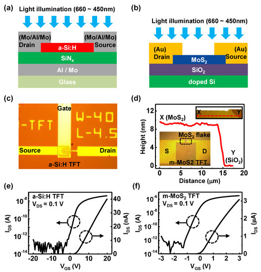
Figure 1.
Cross-sectional views of (a) an a-Si:H TFT and (b) a m-MoS2 TFT under illumination. Optical microscope images of (c) an implemented a-Si:H TFT. (d) Topographical cross-sectional profile along the dashed line indicates in the atomic force a microscope image of exfoliated MoS2 layers, X on thermal oxide and Y in the FETs. X and Y in the inset (right top) denote the location of an oxide (SiO2) and a MoS2 layer, respectively. Inset (left bottom) shows optical microscope images of the implemented m-MoS2 TFT. The channel width-to-length ratio (W/L) was 40/4.5 μm for the a-Si:H TFT and 30/10 μm for the m-MoS2 TFT. Transfer characteristics of (e) a-Si:H TFT and (f) m-MoS2 TFT in linear and log scale measured at VDS = 0.1 V.
For n-type doping, poly-L-lysine (PLL) was purchased from Sigma–Aldrich (Seoul, Korea) and used as charge enhancing molecules for the m-MoS2 TFTs. For the treatment, the fabricated m-MoS2 TFTs were dipped in a water solution containing PLL (0.1% w/v) in ambient air, at room temperature. The dipping time was 2.5 h for the PLL treatment, followed by baking at 100 °C on a hot plate for 10 min. A Raman spectrometer (WITEC alpha300, Ulm, Germany) was used to analyze the Raman spectra and PL intensity of the TMDC flakes with a 532 nm laser excitation and 1 μm of beam size. Light for comparison of the photo response between a-Si:H and m-MoS2 TFTs was illuminated by the laser (wavelength: 630 nm, 530 nm, and 450 nm; power: 1 μW~20 mW) and a multi-wavelength fiber-coupled LED source (Mightex, Inc., Pleasanton, CA, USA) with various wavelength (365 nm, 455 nm, 530 nm, 656 nm, and 740 nm), and 3 mW cm−2 of power density was employed to measure the photocurrent of m-MoS2 TFTs before and after PLL treatment. All the electrical characterizations were measured with a semiconductor impedance analyzer (Agilent 4155C, Seoul, Korea) in ambient air at room temperature.
3. Results and Discussion
3.1. Comparative Study on the Photoresponse of a-Si:H and m-MoS2 TFTs
Figure 1e,f display the transfer characteristics (IDS–VGS) of implemented a-Si:H TFTs and m-MoS2 TFTs at VDS = 0.1 V. The on/off current ratio was ~106 for the a-Si:H TFT and ~107 for the m-MoS2 TFT. The field-effect mobility (μFE) was, respectively, extracted as 0.34 and 12.36 cm2/V·s for a-Si:H and m-MoS2 TFTs from the equation μFE = gm·L/(COX·VDS·W), where gm is the transconductance, COX is the dielectric capacitance, L and W indicate channel length and width, and VDS·is drain-to-source voltage, respectively. The subthreshold swing (SS) of the m-MoS2 transistor was ~200 mV/dec, while it was 1 V/dec with the a-Si:H TFTs. The extracted electrical properties indicate that the quality of fabricated TFTs was reasonable compared with previous results in the literature [31,37,38,39]; thus, the photoresponse of both TFTs were ready to be compared without consideration of noticeable defects or flaws.
For a fair comparison, both TFTs had similar channel dimensions, the distance between light source and device was fixed, and the duration of illuminated light was identically set. Then, to investigate the photoelectrical properties of the a-Si:H and m-MoS2 TFTs, the transfer characteristics under illumination with different wavelength and intensities were measured. Figure 2a–c show photo-induced transfer curves at VDS = 0.1 V, obtained from a-Si:H TFT in log scale, and their linear scale is shown in Figure 2d–f. Power intensity varies from 1 μW to 20 mW for 660 nm laser, from 1 μW to 5 mW for 530 nm laser, and from 10 μW to 5 mW for 450 nm laser. Measured data, as shown in Figure 2, revealed the generation of photocurrent (Iphoto = Ilight − Idark) of a-Si:H TFTs under illumination, corresponding to all wavelengths in this test. The generation of a photocurrent can be explained according to the following scenario: when the light illuminated the channel materials, photon energy of light produced the electron–hole pairs in the channel region. Then, the excited electron–hole pairs drifted along the channel by the applied lateral E-field associated with VDS, resulting in the increase of drain-to-source current. In addition, the photocurrent of a-Si:H was enhanced as the light intensity increased, that is, a stronger optical power generates more electron–hole pairs from the channel materials. Figure 2 presents a proper photo-transistor operation of a-Si:H TFTs, and the linear scale graphs indicate a gradual photocurrent increase at the on-state (VGS > 0 V) without degradation of the field-effect mobility. With the same procedures for the evaluation of the photoresponse, Figure 3 shows the transfer characteristics of the m-MoS2 TFTs under illumination with different wavelength and intensities. The m-MoS2 TFTs also exhibit proper photo-transistor operation, and a parallel shift of Vth was observed in the linear scale graphs. When we visually compared the photoresponse for both TFTs, it can be directly seen that the photocurrent of the a-Si:H TFTs was at an nA level, whereas the m-MoS2 TFTs was at a μA level. Furthermore, the m-MoS2 TFTs had a sensitive dependency on the wavelength of light, and these photoresponses can be potentially tailored by engineering the layer thickness [40,41]. Thus, these results elucidate a better potential of MoS2 for the versatile and high-performance photodetectors.
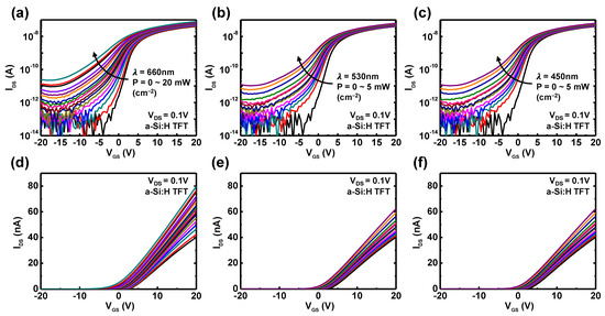
Figure 2.
Transfer characteristics of a-Si:H TFTs under illumination of 660, 530, and 450 nm lasers in (a–c) log and (d–f) linear scale. Various optical intensities (0~5 mW cm–2) were applied to a-Si:H TFTs with the same distance and angle.
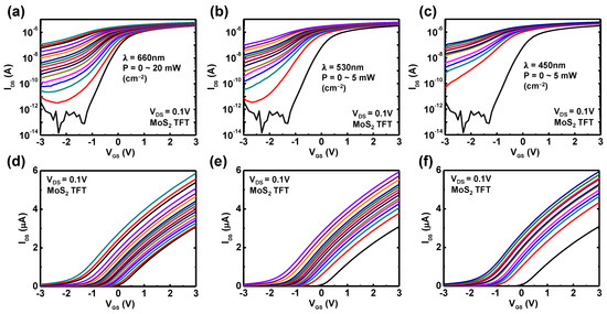
Figure 3.
Transfer characteristics of m-MoS2 TFTs under illumination at 660, 530, and 450 nm using lasers in (a–c) log and (d–f) linear scale at VDS = 0.1 V. Various optical intensities (0~5 mW cm–2) were applied to a-Si:H TFTs with the same distance and angle.
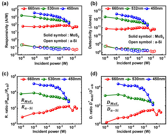
One of the most important figures of merit for a photodetector is its external photoresponsivity and detectivity. To quantitatively compare the performance of photoresponse, both photoresponsivity and detectivity were extracted and shown in Figure 4. The photoresponsivity and detectivity were calculated from equations R = Iphoto/Plight, D = R × S1/2(2qIdark)1/2, where P is a total incident optical power, S is the effective illuminated area, q is the electron charge, and Idark is dark current. Iphoto and Idark are the current levels in the off regime, for the bias condition, at VGS = −1.2 V for m-MoS2 TFTs and VGS = −1.5 V for a-Si:H TFTs, respectively, under either light illumination or dark condition. Figure 4a shows extracted photoresponsivity of m-MoS2 and a-Si:H TFTs. The photoresponsivities of the m-MoS2 TFTs ranged from 102 to 104 for RGB light, and those of the a-Si:H TFTs were within 10−1, wherein the responsivities of the a-Si:H TFTs were similar regardless of the wavelength as reported in the literature [31]. In the all of wavelengths and optical power ranges, the m-MoS2 TFTs exhibited 2~5 orders larger responsivities than that of the a-Si:H TFTS, which is attributed to different photocurrent value for both TFTs. In addition, Figure 4b presents the detectivity of the m-MoS2 and a-Si:H TFTs, from which detectivities of the m-MoS2 TFTs were 1011~1013 and those of the a-Si:H TFTs were extracted as 108~109. Due to the noticeable current ratio between Iphoto and Idark, the m-MoS2 TFTs had clearly higher detectivities than a-Si:H TFTs. As a result, in the all of wavelength and optical power range, the m-MoS2 TFTs exhibited 2~4 orders larger detectivities. The overall quantitative comparison of responsivities and detectivities for the m-MoS2 and a-Si:H TFTs are summarized in Figure 4c,d, which obviously confirms a much better performance of MoS2 photodetector.
In addition, as a circuit level photodetector, photosensitive inverters were implemented and compared using a-Si:H and m-MoS2 TFTs in Figure 5. These photoinverters are key component of light-to-frequency conversion circuits (LFCs), which are practically beneficial for the future IoT systems required for a high level of security [37,38,39,42]. To demonstrate the capabilities of a-Si:H and m-MoS2 TFTs in a circuit-level photodetector, the photo response of depletion load enhancement driver (DLED) inverters was measured. In the configuration of an a-Si:H DLED inverter, the channel width of the load TFT (Wload) was varied to change the effective illuminated area of the a-Si:H channel under light illumination. Figure 5a displays the voltage transfer characteristics (VTCs) of an a-Si:H DLED inverter with 40 μm of Wload. In dark conditions, the switching behavior of the inverter was poor, whereas it is improved under light illumination. This is because sufficient load currents are required to obtain reasonable swing performance in VTCs for a DLED inverter. Thus, under illumination, increased currents yielded improved switching behaviors. However, in this case, VTC curves were not distinguished depending on different wavelength of light (i.e., R, G, B), so that the requirements of photosensitive inverters were not satisfied. To secure sufficient load currents, a-Si:H DLED inverters with large Wload of 4000 and 8000 μm were utilized. As shown in Figure 5b,c, in dark conditions, decent switching properties were obtained with 4000 μm Wload and full swing characteristics were achieved with 8000 μm Wload. Furthermore, minimum VOUT (VOL) values did not reach the value of zero due to the fact of too much photocurrent stemming from a large illuminating area; thus, there waw a tradeoff between the stability of the inverter operation and photoresponse. On the contrary, the DLED inverter composed of m-MoS2 TFTs with 30 m Wload exhibited stable full-swing characteristics under dark and illumination at all wavelengths, which is attributed to better mobility and photoresponse than the a-Si:H TFTs. Consequently, Figure 5 indicates that the a-Si:H TFTs require at least 8000 μm of channel width for the application of photosensitive inverters, compared to the 30 μm of the m-MoS2 TFTs. These results elucidate that m-MoS2 TFTs have robust advantages with regard to the level of device integration per area, chip density, and sensitive modulation properties in variations of wavelength from dark to blue compared to the a-Si:H TFTs.
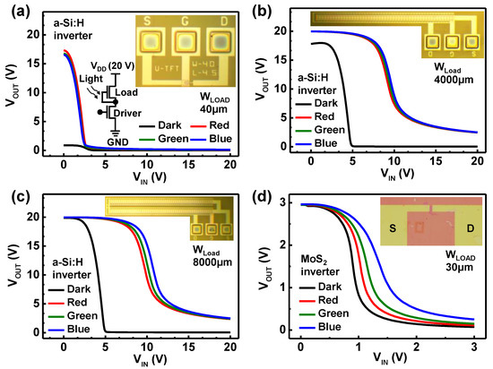
Figure 5.
Voltage transfer characteristics of a-Si:H DLED inverters with (a) 40 μm, (b) 4000 μm, and (c) 8000 μm of Wload under illumination from dark to blue. (d) Voltage transfer characteristics of m-MoS2 DLED inverters with 30 μm Wload. Insets show optical image of a-Si:H and m-MoS2 TFTs with each channel dimension.
3.2. Improvement in the Photoresponse of m-MoS2 TFTs by Molecular Doping Technique
In addition to revealing the high optoelectrical performance of m-MoS2 TFTs by comparison with a-Si:H TFTs, the photoresponsivity can be enhanced by molecular doping treatment [43,44,45]. Although there are different techniques to improve the photodetector’s performance, the molecular doping method has several advantages, as it does not need a change in the device’s structure or the addition of different channel materials or layers but consist of a low temperature process, ultra-thin thickness, and post-process compatibility after device fabrication. In this regard, poly-L-lysine (PLL) was adopted to enhance the photoresponsivity via n-doping effect for m-MoS2 TFTs from PLL molecules.
Figure 6a illustrates a schematic for molecular doping of m-MoS2 TFT to induce donor-like doping with facilitation of charge enhancers. Attached on the surface of m-MoS2, amine (NH2)-based charge transfer of PLL molecules can play a role in donating electrons toward MoS2 layers, leading to donor-like doping effects with protonated NH3+ functional group in PLL. Figure 1b shows transfer characteristics of m-MoS2 TFTs at VDS = 1 V in log and linear scale, respectively. After the PLL treatment for 1.5 h, without discernible degradation of SS and of-off ratio, clear Vth shift (ΔVth ~ −1.0 V) and improvement of on-current were shown. For the quantitative analysis on doping effects according to the PLL treatment, mobility, and carrier concentration was plotted in Figure 6c. The carrier concentration was calculated by the following equation n2D = (L/W) (IDS/q·μFE·VDS), where L and W are the length and width of channel and q is the electron charge. As a consequence of charge enhancement, μFE was extracted as 13.0 and 18.3 cm2/V·s before and after PLL treatment, respectively, which reveals a 40% increase in μFE. In parallel, n2D was calculated as 2.0 × 10¹² and 2.4 × 10¹² before and after PLL treatment, respectively, from which 20% enhancement of n2D was obtained. These results clearly show the improvement of electrical properties by treatment of PLL.
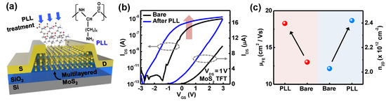
Figure 6.
(a) A schematic illustration of m-MoS2 TFTs with PLL molecules treated on the surface of m-MoS2; (b) transfer characteristics of m-MoS2 TFTs at VDS = 1 V before and after PLL treatment; (c) extracted field effect mobility and carrier concentration before and after PLL treatment.
Thereafter, for better understanding on electrically observed doping effects by PLL, chemical and physical properties and their analysis on m-MoS2 TFTs were examined. First, optical properties were examined via photoluminescence (PL) spectroscopy. Figure 7a shows PL spectra of m-MoS2 TFTs after PLL treatment, from which peak intensity after PLL treatment was reduced because donor-like doping effects enhanced the formation of tightly bound trions of MoS2 [45,46,47], leading to a decrease in the radiative recombination of excitons. With the extracted optical properties, electrical behaviors, corresponding to each optical excitation, were investigated in the following section. As reported elsewhere [45,47,48,49,50,51,52,53,54], Raman spectroscopy also has been dominantly used as a reliable tool to confirm the doping effects on TMDCs. Figure 4a plots the Raman spectra of the m-MoS2 TFTs before and after the treatment of PLL. In the Figure 4a, two characteristic vibrational modes (E12g and A1g) were observed near 383 and 409 cm−1 in the bare m-MoS2 flakes, where E12g mode was attributed to the in-plane vibration between Mo and S atoms, whereas the A1g mode was due to the out-of-plane vibration between Mo and S atoms. After the PLL treatment, the E12g and A1g peaks were shifted left by 0.25 cm−1 and 0.63 cm−1 for m-MoS2 TFTs, respectively. Obviously observed left shifts of two characteristics mode in Raman peaks describe that n-doping effects of PLL treatment result from the increase of the electron–phonon scattering due to the higher electron concentration [45,47,48,49,51,52,55]. Thus, PLL treatment would enhance the electron density, leading to increase of electron–phonon scattering, which lends phonon frequency decreased [54]. The Raman results support the n-doping effects on m-MoS2 TFTs, which are attributed to the PLL treatment, and their chemical analysis via Raman nicely matched with the entire trend of electrical properties as shown in Figure 6.
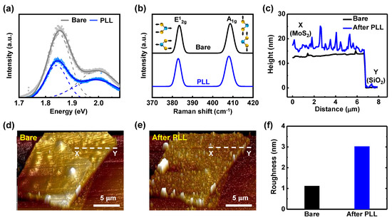
Figure 7.
(a) Photoluminescence (PL) characteristics of m-MoS2 flakes before and after PLL treatment; (b) evolution of Raman spectra of m-MoS2 corresponding to bare condition and PLL treatment; (c) Height profile of m-MoS2 flakes measured by AFM before and after PLL treatment. X and Y denote MoS2 and SiO2 region, respectively; (d) AFM topographical images of m-MoS2 flake for (d) bare condition and (e) PLL treatment. Dashed line indicates extracted points to obtain height profile in Figure 7c; (f) evolution of surface roughness of the m-MoS2 flakes extracted from the AFM topography. The Surface roughness increased via attached molecules after PLL treatment.
In addition, as for the physical examination, morphological change of m-MoS2 flakes by PLL treatment was measured by atomic force microscopy (AFM). Figure 7c–e display the height information and AFM 3D images of MoS2 flake before and after PLL treatment for 3 h. Figure 7c reveals the increased height profile of MoS2 flake along the flake-substrate line, which is attributed to attached PLL molecules on the surface of MoS2 flake. The position of X (MoS2) and Y (SiO2) measured by AFM are denoted in Figure 7d,e. Moreover, the images of Figure 7d,e show the bare and PLL-treated MoS2 flake, respectively, where the bumpy surface of MoS2 flakes was slightly observed after PLL treatment. Thereafter, as a root mean square (RMS) value, surface roughness by AFM analysis was extracted as 1.12 nm (or 3.03 nm) for MoS2 flakes before (or after) PLL treatment for 3 h, respectively (Figure 4f). All results in Figure 7c–f are one of reasonable evidence to validate that the attachment of PLL molecules enables to modify nano-scaled surface morphology of MoS2 flake [51,56], resulting in possible tuning of electrical properties for m-MoS2 FFTs.
To validate the doping effects on improvement of photoresponse, variations of currents under illumination were monitored before and after PLL treatment. Figure 8a presents transfer characteristics (e.g., 3-terminal operation) of the m-MoS2 TFTs without any doping treatment. Under illumination from the visible to UV range (740~365 nm), an increase in currents was observed in the bare m-MoS2 TFTs, which are commonly reported behaviors in the literature [37,38,39,40]. Furthermore, an increase in the current was gradually enhanced as the wavelength of the light decrease (i.e., as photon energy increase) [37,38,39,40]. Thereafter, time-dependent photoresponse in two-terminal operation was measured. Figure 8b shows photocurrents of bare m-MoS2 TFTs at VDS = 1 V. As similar with transfer characteristics in Figure 8a, increases in the photocurrent are gradually shown as the wavelengths of the light decreased. Then, after PLL treatment for bare the m-MoS2 TFTs, the photoresponses were measured with same condition. Figure 8c displays the transfer characteristics of the PLL treated the m-MoS2 TFTs. It is shown that after PLL treatment, the transfer curves shifted left in dark conditions, compared to the bare m-MoS2 TFTs. Moreover, the currents of the PLL-treated m-MoS2 TFTs under illumination were also higher than those of the bare m-MoS2 TFTs, which might be attributed to enhancement of the photoresponse. However, the increased currents of the PLL-treated m-MoS2 TFTs under illumination than the bare m-MoS2 TFTs might be regarded as only the results of Vth shift. Therefore, to clearly confirm the improvement in the photoresponse, photocurrents were extracted in Figure 8d. The larger photocurrents of the PLL-treated m-MoS2 TFTs were evidently observed under all wavelength ranges. In addition, the μFE of the bare m-MoS2 TFTs was augmented at 33% under illumination of 365 nm compared to dark conditions, whereas the PLL-treated m-MoS2 TFTs had a 92% enhanced μFE under illumination of 365 nm. Lastly, responsivity and detectivity were examined as quantitative evaluations of photoresponse. Figure 8e presents 2~6 times higher responsivities and 1.3~3.5 times enlarged detectivities of the PLL-treated m-MoS2 TFTs, compared to the bare m-MoS2 TFTs. These behaviors are well matched with previous results [43,44,45,47]. As a result, Figure 8 validates the improved photoresponse of the m-MoS2 TFTs after PLL treatment, which is possibly due to the increased number of tightly bound trions and their lifetime as shown in Figure 7a [46,57].
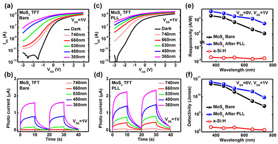
Figure 8.
Photoresponses from (a) transfer characteristics and (b) two-terminal output characteristics of bare m-MoS2 TFTs under illumination from 740 nm to 365 nm. Photoresponses from (c) transfer characteristics and (d) two-terminal output characteristics of PLL-treated m-MoS2 TFTs. Comparisons of (e) responsivities and (f) detectivities of bare and PLL-treated m-MoS2 TFTs and a-Si:H TFTs extracted at VGS = 0 V, VDS = 1 V for wavelength from 740 nm to 365 nm.
In addition, the response and recovery time for the m-MoS2 and a-Si:H TFTs were extracted at 90% and 10% of maximum photo current. Overall, bare m-MoS2 TFTs had a rise (or decay) time in the range from 3.5 (or 6.1) to 7.4 (or 6.9) s, respectively, under wavelengths from 365 to 740 nm, whereas PLL-treated m-MoS2 TFTs possessed rise (or decay) time from 2.6 (or 7.9) to 6.1 (or 9.8) sec of rise time, respectively. The shortened response time and prolonged recovery time might be attributed to the enhanced formation of tightly bound trions with PLL treatment in the m-MoS2 TFTs [46], leading to a decreased recombination rate of excitons. Reduced PL intensities of the m-MoS2 TFTs with PLL treatment supports the decreased recombination rate of excitons as shown in Figure 7a. Therefore, the prolonged lifetime of carriers can induce faster response times of photoexcited carriers and their slower recovery time with PLL treatment. However, response and recovery time of a-Si:H TFTs were extracted within a 10 ms range, which is consistent with other literature [31]. Thus, response and recovery time of the m-MoS2 TFTs remained as a problem to be resolved yet. This should be accompanied with an improvement of material, insulator, and passivation, and interface engineering.
Overall, the performance of m-MoS2 photodetector itself is not overwhelmed, as compared with the previously reported data in the literature. However, in this study, it is meaningful that the development of generally applicable doping methodology for performance improvement of TMDC photodetectors and its comparative study with conventional products of a-Si:H TFTs in order to understand the figures of merit quantitatively. The present works could provide the intuitive criteria from the perspective of researchers in terms of key aspects that are required for MoS2 layers as one of the next-generation semiconductors for the future photodetectors in display systems.
4. Conclusions
In this study, a comparative study of the photoresponse of m-MoS2 and a-Si:H TFTs was conducted to provide better insight into the photodetector performances of m-MoS2 TFTs as photosensors integrated with display systems. With extracted 2~4 orders larger photo responsivity and detectivity of m-MoS2 TFTs, it revealed better performance of m-MoS2 photodetectors in the various wavelengths and optical power ranges. Furthermore, the photosensitive m-MoS2 DLED inverter showed robust advantages with regard to level of device integration per area, chip density, and sensitive modulation properties in variations of wavelength from dark to blue as compared to an a-Si:H DLED inverter. In addition, as a strategy to improve the field effect mobility and photoresponse of the m-MoS2 TFTs, molecular doping by PLL treatment was applied to the m-MoS2 TFTs. Transfer and output characteristics of the m-MoS2 TFTs clearly showed improved photocurrent generation under a wide range of illuminations (740~365 nm), and its chemical and physical properties were analyzed by XPS, Raman spectroscopy, and AFM to confirm the doping effects on m-MoS2 TFTs. As a result, along with extracted photo responsivity and detectivity, PLL treatment demonstrated not only the ability to induce n-doping effects but also to improve the photoresponse of the m-MoS2 TFTs. This comparative study will provide an intuitive criteria for m-MoS2 TFTs to be utilized as future photodetectors in flat panel displays, and it will make them more attractive with their potential for high-performance photodetection enabled by a novel doping technique.
Author Contributions
Conceptualization, S.H.J.; methodology, S.H.J.; validation, S.G.S. and J.H.R.; Formal analysis, S.G.S. and J.H.R.; investigation, S.G.S., J.H.R., S.Y.K., and J.J.; resources, S.H.J.; data curation, S.G.S. and J.H.R.; writing—original draft preparation, S.G.S. and J.H.R.; writing—review and editing, S.G.S., J.H.R., S.Y.K., and J.J.; visualization, S.G.S. and J.H.R.; supervision, S.H.J.; project administration, S.H.J.; funding acquisition, S.H.J. All authors have read and agreed to the published version of the manuscript.
Funding
This work was supported by the Incheon National University Research Grant in 2019.
Data Availability Statement
The data presented in this study are available on request from the corresponding author.
Conflicts of Interest
The authors declare no conflict of interest. The funders had no role in the design of the study; in the collection, analyses, or interpretation of data; in the writing of the manuscript, or in the decision to publish the results.
References
- Roy, M.; Mukhopadhyay, S.; Mahmoodi-Meimand, H. Leakage current mechanisms and leakage reduction techniques in deep-submicrometer CMOS circuits. Proc. IEEE 2003, 91, 305–327. [Google Scholar] [CrossRef]
- Abbas, Z.; Olivieri, M. Impact of technology scaling on leakage power in nano-scale bulk CMOS digital standard cells. Microelectron. J. 2014, 45, 179–195. [Google Scholar] [CrossRef]
- Wang, Q.H.; Kalantar-Zadeh, K.; Kis, A.; Coleman, J.N.; Strano, M.S. Electronics and optoelectronics of two-dimensional transition metal dichalcogenides. Nat. Nanotechnol. 2012, 7, 699–712. [Google Scholar] [CrossRef] [PubMed]
- Jariwala, D.; Sangwan, V.K.; Lauhon, L.J.; Marks, T.J.; Hersam, M.C. Emerging device applications for semiconducting two-dimensional transition metal dichalcogenides. ACS Nano 2014, 8, 1102–1120. [Google Scholar] [CrossRef] [PubMed]
- Desai, S.B.; Madhvapathy, S.R.; Sachid, A.B.; Llinas, J.P.; Wang, Q.; Ahn, G.H.; Pitner, G.; Kim, M.J.; Bokor, J.; Hu, C.; et al. MoS2 transistors with 1-nanometer gate lengths. Science 2016, 354, 99–102. [Google Scholar] [CrossRef]
- Chhowalla, M.; Shin, H.S.; Eda, G.; Li, L.J.; Loh, K.P.; Zhang, H. The chemistry of two-dimensional layered transition metal dichalcogenide nanosheets. Nat. Chem. 2013, 5, 263–275. [Google Scholar] [CrossRef]
- Venkata Subbaiah, Y.P.; Saji, K.J.; Tiwari, A. Atomically Thin MoS2: A Versatile Nongraphene 2D Material. Adv. Funct. Mater. 2016, 26, 2046–2069. [Google Scholar] [CrossRef]
- Radisavljevic, B.; Radenovic, A.; Brivio, J.; Giacometti, V.; Kis, A. Single-layer MoS2 transistors. Nat. Nanotechnol. 2011, 6, 147–150. [Google Scholar] [CrossRef]
- Jariwala, D.; Sangwan, V.K.; Late, D.J.; Johns, J.E.; Dravid, V.P.; Marks, T.J.; Lauhon, L.J.; Hersam, M.C. Band-like transport in high mobility unencapsulated single-layer MoS2 transistors. Appl. Phys. Lett. 2013, 102, 173107. [Google Scholar] [CrossRef]
- He, G.; Ghosh, K.; Singisetti, U.; Ramamoorthy, H.; Somphonsane, R.; Bohra, G.; Matsunaga, M.; Higuchi, A.; Aoki, N.; Najmaei, S.; et al. Conduction Mechanisms in CVD-Grown Monolayer MoS2 Transistors: From Variable-Range Hopping to Velocity Saturation. Nano Lett. 2015, 15, 5052–5058. [Google Scholar] [CrossRef] [PubMed]
- Wang, H.; Yu, L.; Lee, Y.H.; Shi, Y.; Hsu, A.; Chin, M.L.; Li, L.J.; Dubey, M.; Kong, J.; Palacios, T. Integrated circuits based on bilayer MoS2 transistors. Nano Lett. 2012, 12, 4674–4680. [Google Scholar] [CrossRef]
- Yu, S.; Kim, J.S.; Jeon, P.J.; Ahn, J.; Park, J.C.; Im, S. Transition Metal Dichalcogenide-Based Transistor Circuits for Gray Scale Organic Light-Emitting Displays. Adv. Funct. Mater. 2017, 27, 1603682. [Google Scholar] [CrossRef]
- Kumar, R.; Kulriya, P.K.; Mishra, M.; Singh, F.; Gupta, G.; Kumar, M. Highly selective and reversible NO2 gas sensor using vertically aligned MoS2 flake networks. Nanotechnology 2018, 29, 464001. [Google Scholar] [CrossRef]
- Gao, G.; Yu, J.; Yang, X.; Pang, Y.; Zhao, J.; Pan, C.; Sun, Q.; Wang, Z.L. Triboiontronic Transistor of MoS2. Adv. Mater. 2019, 31, 1806905. [Google Scholar] [CrossRef]
- Yang, X.; Han, J.; Yu, J.; Chen, Y.; Zhang, H.; Ding, M.; Jia, C.; Sun, J.; Sun, Q.; Wang, Z.L. Versatile Triboiontronic Transistor via Proton Conductor. ACS Nano 2020, 14, 8668–8677. [Google Scholar] [CrossRef] [PubMed]
- Yang, X.; Yu, J.; Zhao, J.; Chen, Y.; Gao, G.; Wang, Y.; Sun, Q.; Wang, Z.L. Mechanoplastic Tribotronic Floating-Gate Neuromorphic Transistor. Adv. Funct. Mater. 2020, 30, 2002506. [Google Scholar] [CrossRef]
- Huang, C.Y.; Chang, C.; Lu, G.Z.; Huang, W.C.; Huang, C.S.; Chen, M.L.; Lin, T.N.; Shen, J.L.; Lin, T.Y. Hybrid 2D/3D MoS2/GaN heterostructures for dual functional photoresponse. Appl. Phys. Lett. 2018, 112, 233106. [Google Scholar] [CrossRef]
- Nalwa, H.S. A review of molybdenum disulfide (MoS2) based photodetectors: From ultra-broadband, self-powered to flexible devices. RSC Adv. 2020, 10, 30529–30602. [Google Scholar] [CrossRef]
- Choi, M.; Park, Y.J.; Sharma, B.K.; Bae, S.R.; Kim, S.Y.; Ahn, J.H. Flexible active-matrix organic light-emitting diode display enabled by MoS2 thin-film transistor. Sci. Adv. 2018, 4, eaas8721. [Google Scholar] [CrossRef] [PubMed]
- Choi, M.; Bae, S.R.; Hu, L.; Hoang, A.T.; Kim, S.Y.; Ahn, J.H. Full-color active-matrix organic light-emitting diode display on human skin based on a large-Area MoS2 backplane. Sci. Adv. 2020, 6, eabb5898. [Google Scholar] [CrossRef] [PubMed]
- Choi, W.; Cho, M.Y.; Konar, A.; Lee, J.H.; Cha, G.B.; Hong, S.C.; Kim, S.; Kim, J.; Jena, D.; Joo, J.; et al. High-detectivity multilayer MoS2 phototransistors with spectral response from ultraviolet to infrared. Adv. Mater. 2012, 24, 5832–5836. [Google Scholar] [CrossRef]
- Kim, K.S.; Ji, Y.J.; Kim, K.H.; Choi, S.; Kang, D.H.; Heo, K.; Cho, S.; Yim, S.; Lee, S.; Park, J.H.; et al. Ultrasensitive MoS2 photodetector by serial nano-bridge multi-heterojunction. Nat. Commun. 2019, 10, 4701. [Google Scholar] [CrossRef]
- Zhang, K.; Peng, M.; Yu, A.; Fan, Y.; Zhai, J.; Wang, Z.L. A substrate-enhanced MoS2 photodetector through a dual-photogating effect. Mater. Horiz. 2019, 6, 826–833. [Google Scholar] [CrossRef]
- Chen, S.; Cao, R.; Chen, X.; Wu, Q.; Zeng, Y.; Gao, S.; Guo, Z.; Zhao, J.; Zhang, M.; Zhang, H. Anisotropic Plasmonic Nanostructure Induced Polarization Photoresponse for MoS2-Based Photodetector. Adv. Mater. Interfaces 2020, 7, 1902179. [Google Scholar] [CrossRef]
- Tsai, D.S.; Liu, K.K.; Lien, D.H.; Tsai, M.L.; Kang, C.F.; Lin, C.A.; Li, L.J.; He, J.H. Few-layer MoS2 with high broadband photogain and fast optical switching for use in harsh environments. ACS Nano 2013, 7, 3905–3911. [Google Scholar] [CrossRef]
- Son, Y.; Wang, Q.H.; Paulson, J.A.; Shih, C.J.; Rajan, A.G.; Tvrdy, K.; Kim, S.; Alfeeli, B.; Braatz, R.D.; Strano, M.S. Layer number dependence of MoS2 photoconductivity using photocurrent spectral atomic force microscopic imaging. ACS Nano 2015, 9, 2843–2855. [Google Scholar] [CrossRef]
- Reynolds, M.F.; Guimarães, M.H.D.; Ga, H.; Kang, K.; Cortese, A.J.; Ralph, D.C.; Park, J.; McEuen, P.L. MoS2 pixel arrays for real-time photoluminescence imaging of redox molecules. Sci. Adv. 2019, 5, eaat9476. [Google Scholar] [CrossRef] [PubMed]
- Snell, A.J.; Mackenzie, K.D.; Spear, W.E.; LeComber, P.G.; Hughes, A.J. Application of amorphous silicon field effect transistors in addressable liquid crystal display panels. Appl. Phys. 1981, 24, 357–362. [Google Scholar] [CrossRef]
- Karim, K.S.; Nathan, A.; Member, S.; Rowlands, J.A. Readout Circuit for Digital Imaging. IEEE Trans. Electron. Devices 2003, 50, 200–208. [Google Scholar] [CrossRef]
- Lee, K.C.; Moon, S.H.; Berkeley, B.; Kim, S.S. Optical feedback system with integrated color sensor on LCD. Sens. Actuators A Phys. 2006, 130–131, 214–219. [Google Scholar] [CrossRef]
- Ahn, S.E.; Song, I.; Jeon, S.; Jeon, Y.W.; Kim, Y.; Kim, C.; Ryu, B.; Lee, J.H.; Nathan, A.; Lee, S.; et al. Metal oxide thin film phototransistor for remote touch interactive displays. Adv. Mater. 2012, 24, 2631–2636. [Google Scholar] [CrossRef] [PubMed]
- Jang, J.T.; Park, J.; Ahn, B.D.; Kim, D.M.; Choi, S.J.; Kim, H.S.; Kim, D.H. Study on the Photoresponse of Amorphous In-Ga-Zn-O and Zinc Oxynitride Semiconductor Devices by the Extraction of Sub-Gap-State Distribution and Device Simulation. ACS Appl. Mater. Interfaces 2015, 7, 15570–15577. [Google Scholar] [CrossRef] [PubMed]
- Shan, C.; Yang, H.; Han, D.; Zhang, Q.; Ivaska, A.; Niu, L. Water-soluble graphene covalently functionalized by biocompatible poly-L-lysine. Langmuir 2009, 25, 12030–12033. [Google Scholar] [CrossRef]
- Basu, A.K.; Sah, A.N.; Pradhan, A.; Bhattacharya, S. Poly-L-Lysine functionalised MWCNT-rGO nanosheets based 3-d hybrid structure for femtomolar level cholesterol detection using cantilever based sensing platform. Sci. Rep. 2019, 9, 3686. [Google Scholar] [CrossRef] [PubMed]
- Zhang, Y.; Li, J.; Shen, Y.; Wang, M.; Li, J. Poly-L-lysine functionalization of single-walled carbon nanotubes. J. Phys. Chem. B 2004, 108, 15343–15346. [Google Scholar] [CrossRef]
- Roh, J.; Cho, I.T.; Shin, H.; Baek, G.W.; Hong, B.H.; Lee, J.H.; Jin, S.H.; Lee, C. Fluorinated CYTOP passivation effects on the electrical reliability of multilayer MoS2 field-effect transistors. Nanotechnology 2015, 26, 455201. [Google Scholar] [CrossRef]
- Ryu, J.H.; Baek, G.W.; Yu, S.J.; Seo, S.G.; Jin, S.H. Photosensitive full-swing multi-layer MoS2 inverters with light shielding layers. IEEE Electron. Device Lett. 2017, 38, 67–70. [Google Scholar] [CrossRef]
- Seo, S.G.; Han, S.W.; Cha, H.Y.; Yang, S.; Jin, S.H. Light-shield layers free photosensitive inverters comprising GaN-Drivers and multi-layered MoS2-Loads. IEEE Electron. Device Lett. 2019, 40, 107–110. [Google Scholar] [CrossRef]
- Seo, S.G.; Jin, S.H. Photosensitive Complementary Inverters Based on n-Channel MoS2 and p-Channel MoTe2 Transistors for Light-to-Frequency Conversion Circuits. Phys. Status Solidi Rapid Res. Lett. 2019, 13, 1900317. [Google Scholar] [CrossRef]
- Lee, H.S.; Min, S.W.; Chang, Y.G.; Park, M.K.; Nam, T.; Kim, H.; Kim, J.H.; Ryu, S.; Im, S. MoS2 nanosheet phototransistors with thickness-modulated optical energy gap. Nano Lett. 2012, 12, 3695–3700. [Google Scholar] [CrossRef] [PubMed]
- Dileep, K.; Sahu, R.; Sarkar, S.; Peter, S.C.; Datta, R. Layer specific optical band gap measurement at nanoscale in MoS2 and ReS2 van der Waals compounds by high resolution electron energy loss spectroscopy. J. Appl. Phys. 2016, 119, 114309. [Google Scholar] [CrossRef]
- Jeong, J.; Seo, S.G.; Kim, S.Y.; Jin, S.H. Photosensitive Complementary Inverters Composed of n-Channel ReS2 and p-Channel Single-Walled Carbon Nanotube Field-Effect Transistors. Phys. Status Solidi Rapid Res. Lett. 2020, 14, 2000420. [Google Scholar] [CrossRef]
- Jo, S.H.; Park, H.Y.; Kang, D.H.; Shim, J.; Jeon, J.; Choi, S.; Kim, M.; Park, Y.; Lee, J.; Song, Y.J.; et al. Broad Detection Range Rhenium Diselenide Photodetector Enhanced by (3-Aminopropyl)Triethoxysilane and Triphenylphosphine Treatment. Adv. Mater. 2016, 28, 6711–6718. [Google Scholar] [CrossRef] [PubMed]
- Kim, J.; Heo, K.; Kang, D.H.; Shin, C.; Lee, S.; Yu, H.Y.; Park, J.H. Rhenium Diselenide (ReSe2) Near-Infrared Photodetector: Performance Enhancement by Selective p-Doping Technique. Adv. Sci. 2019, 6, 1901255. [Google Scholar] [CrossRef]
- Lin, J.D.; Han, C.; Wang, F.; Wang, R.; Xiang, D.; Qin, S.; Zhang, X.A.; Wang, L.; Zhang, H.; Wee, A.T.S.; et al. Electron-doping-enhanced trion formation in monolayer molybdenum disulfide functionalized with cesium carbonate. ACS Nano 2014, 8, 5323–5329. [Google Scholar] [CrossRef]
- Mak, K.F.; He, K.; Lee, C.; Lee, G.H.; Hone, J.; Heinz, T.F.; Shan, J. Tightly bound trions in monolayer MoS2. Nat. Mater. 2013, 12, 207–211. [Google Scholar] [CrossRef]
- Kang, D.H.; Kim, M.S.; Shim, J.; Jeon, J.; Park, H.Y.; Jung, W.S.; Yu, H.Y.; Pang, C.H.; Lee, S.; Park, J.H. High-Performance Transition Metal Dichalcogenide Photodetectors Enhanced by Self-Assembled Monolayer Doping. Adv. Funct. Mater. 2015, 25, 4219–4227. [Google Scholar] [CrossRef]
- Li, Y.; Xu, C.; Hu, P.; Zhen, L. Carrier Control of MoS2 Nanoflakes by. ACS Nano 2013, 7, 7795–7804. [Google Scholar] [CrossRef]
- Kang, D.H.; Jeon, M.H.; Jang, S.K.; Choi, W.Y.; Kim, K.N.; Kim, J.; Lee, S.; Yeom, G.Y.; Park, J.H. Self-Assembled Layer (SAL)-Based Doping on Black Phosphorus (BP) Transistor and Photodetector. ACS Photonics 2017, 4, 1822–1830. [Google Scholar] [CrossRef]
- Kang, D.H.; Shim, J.; Jang, S.K.; Jeon, J.; Jeon, M.H.; Yeom, G.Y.; Jung, W.S.; Jang, Y.H.; Lee, S.; Park, J.H. Controllable nondegenerate p-type doping of tungsten diselenide by octadecyltrichlorosilane. ACS Nano 2015, 9, 1099–1107. [Google Scholar] [CrossRef]
- Ji, H.G.; Solís-Fernández, P.; Yoshimura, D.; Maruyama, M.; Endo, T.; Miyata, Y.; Okada, S.; Ago, H. Chemically Tuned p- and n-Type WSe2 Monolayers with High Carrier Mobility for Advanced Electronics. Adv. Mater. 2019, 31, 1903613. [Google Scholar] [CrossRef] [PubMed]
- Tarasov, A.; Zhang, S.; Tsai, M.Y.; Campbell, P.M.; Graham, S.; Barlow, S.; Marder, S.R.; Vogel, E.M. Controlled doping of large-area trilayer MoS2 with molecular reductants and oxidants. Adv. Mater. 2015, 27, 1175–1181. [Google Scholar] [CrossRef] [PubMed]
- Cho, K.; Min, M.; Kim, T.Y.; Jeong, H.; Pak, J.; Kim, J.K.; Jang, J.; Yun, S.J.; Lee, Y.H.; Hong, W.K.; et al. Electrical and Optical Characterization of MoS2 with Sulfur Vacancy Passivation by Treatment with Alkanethiol Molecules. ACS Nano 2015, 9, 8044–8053. [Google Scholar] [CrossRef]
- Roh, J.; Ryu, J.H.; Baek, G.W.; Jung, H.; Seo, S.G.; An, K.; Jeong, B.G.; Lee, D.C.; Hong, B.H.; Bae, W.K.; et al. Threshold Voltage Control of Multilayered MoS2 Field-Effect Transistors via Octadecyltrichlorosilane and their Applications to Active Matrixed Quantum Dot Displays Driven by Enhancement-Mode Logic Gates. Small 2019, 15, 1803852. [Google Scholar] [CrossRef]
- Iqbal, M.W.; Amin, A.; Kamran, M.A.; Ateeq, H.; Elahi, E.; Hussain, G.; Azam, S.; Aftab, S.; Alharbi, T.; Majid, A. Tailoring the electrical properties of MoTe2 field effect transistor via chemical doping. Superlattices Microstruct. 2019, 135, 106247. [Google Scholar] [CrossRef]
- Lee, B.; Chen, Y.; Duerr, F.; Mastrogiovanni, D.; Garfunkel, E.; Andrei, E.Y.; Podzorov, V. Modification of electronic properties of graphene with self-assembled monolayers. Nano Lett. 2010, 10, 2427–2432. [Google Scholar] [CrossRef]
- Heo, K.; Jo, S.H.; Shim, J.; Kang, D.H.; Kim, J.H.; Park, J.H. Stable and Reversible Triphenylphosphine-Based n-Type Doping Technique for Molybdenum Disulfide (MoS2). ACS Appl. Mater. Interfaces 2018, 10, 32765–32772. [Google Scholar] [CrossRef]
Publisher’s Note: MDPI stays neutral with regard to jurisdictional claims in published maps and institutional affiliations. |
© 2021 by the authors. Licensee MDPI, Basel, Switzerland. This article is an open access article distributed under the terms and conditions of the Creative Commons Attribution (CC BY) license (https://creativecommons.org/licenses/by/4.0/).