
Electronic Transport Mechanisms Correlated to Structural Properties of a Reduced Graphene Oxide Sponge

 , , ,
, , ,  and
and 
Abstract
:1. Introduction
2. Experimental
3. Results
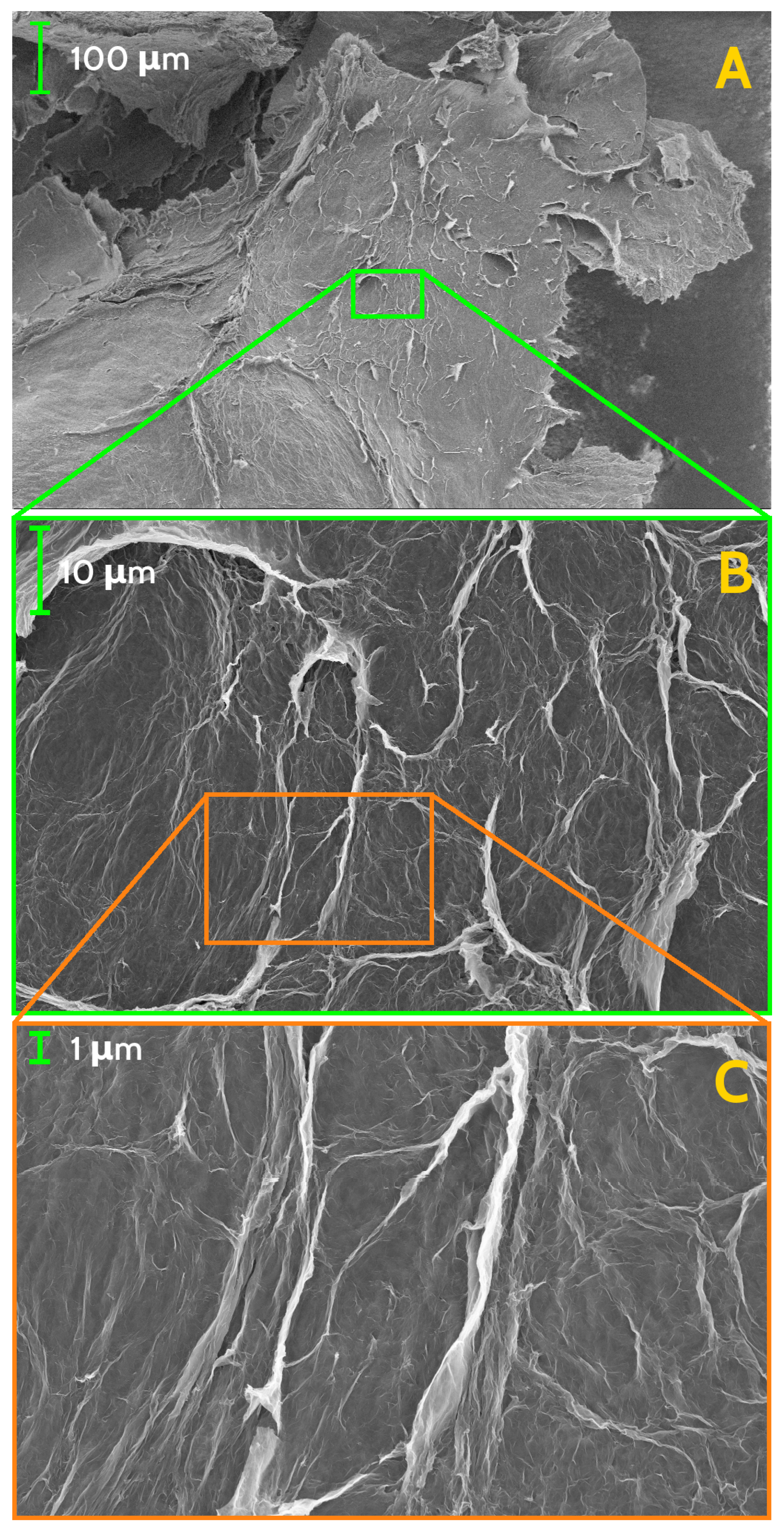
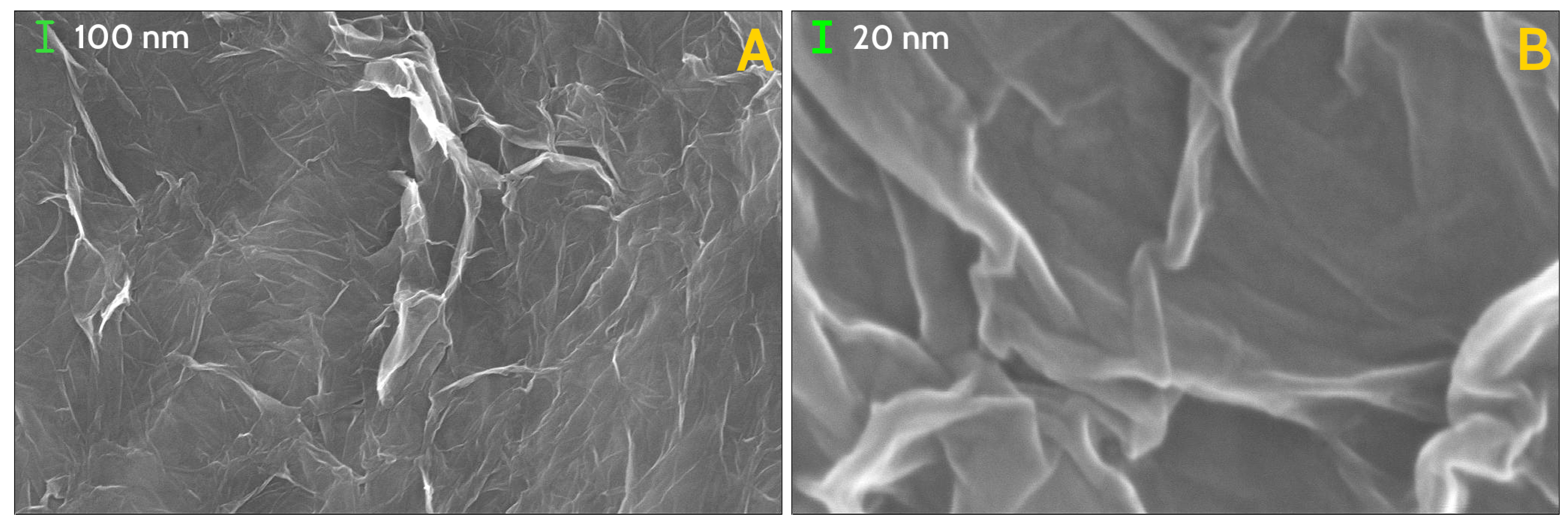
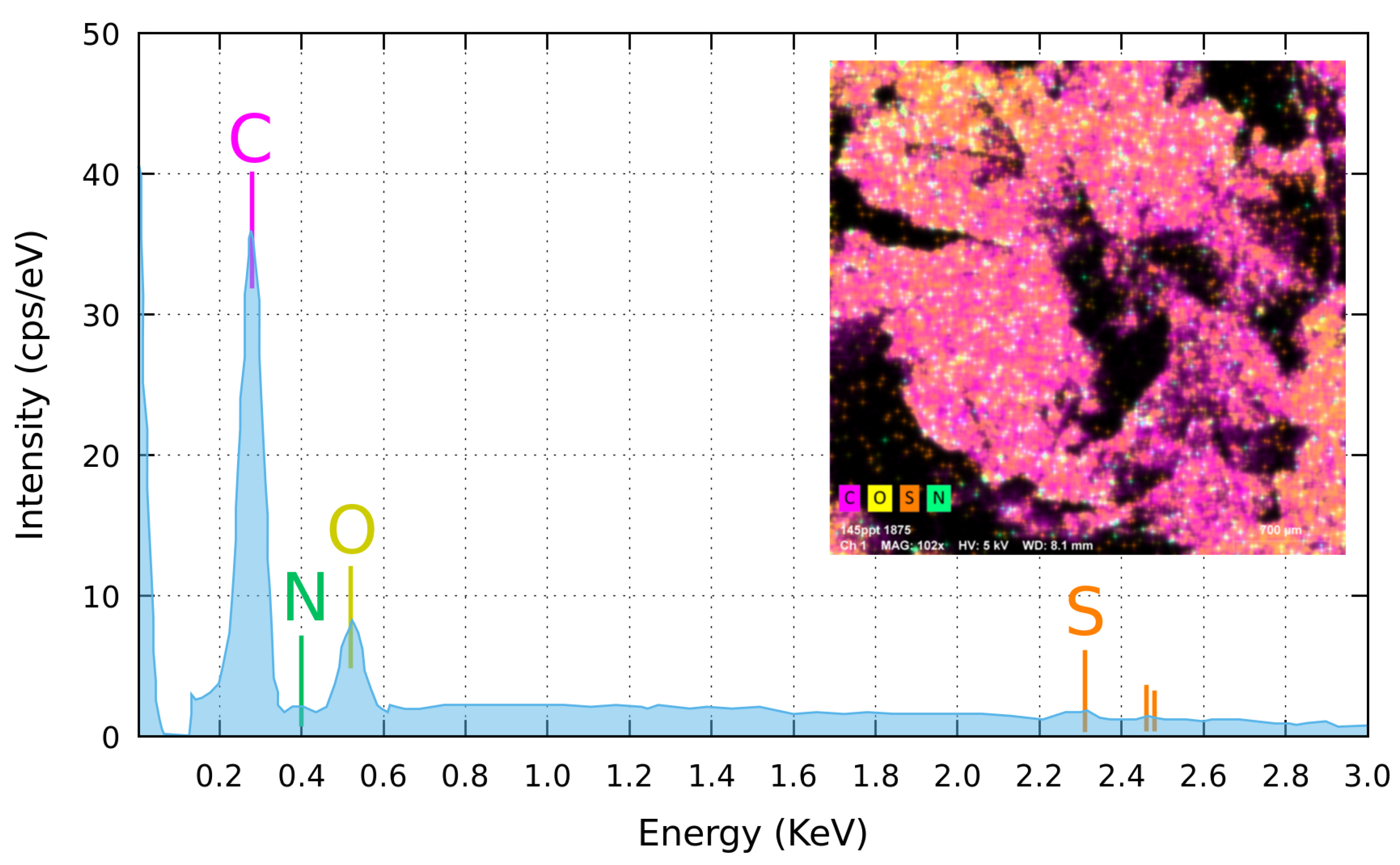
3.1. Structure
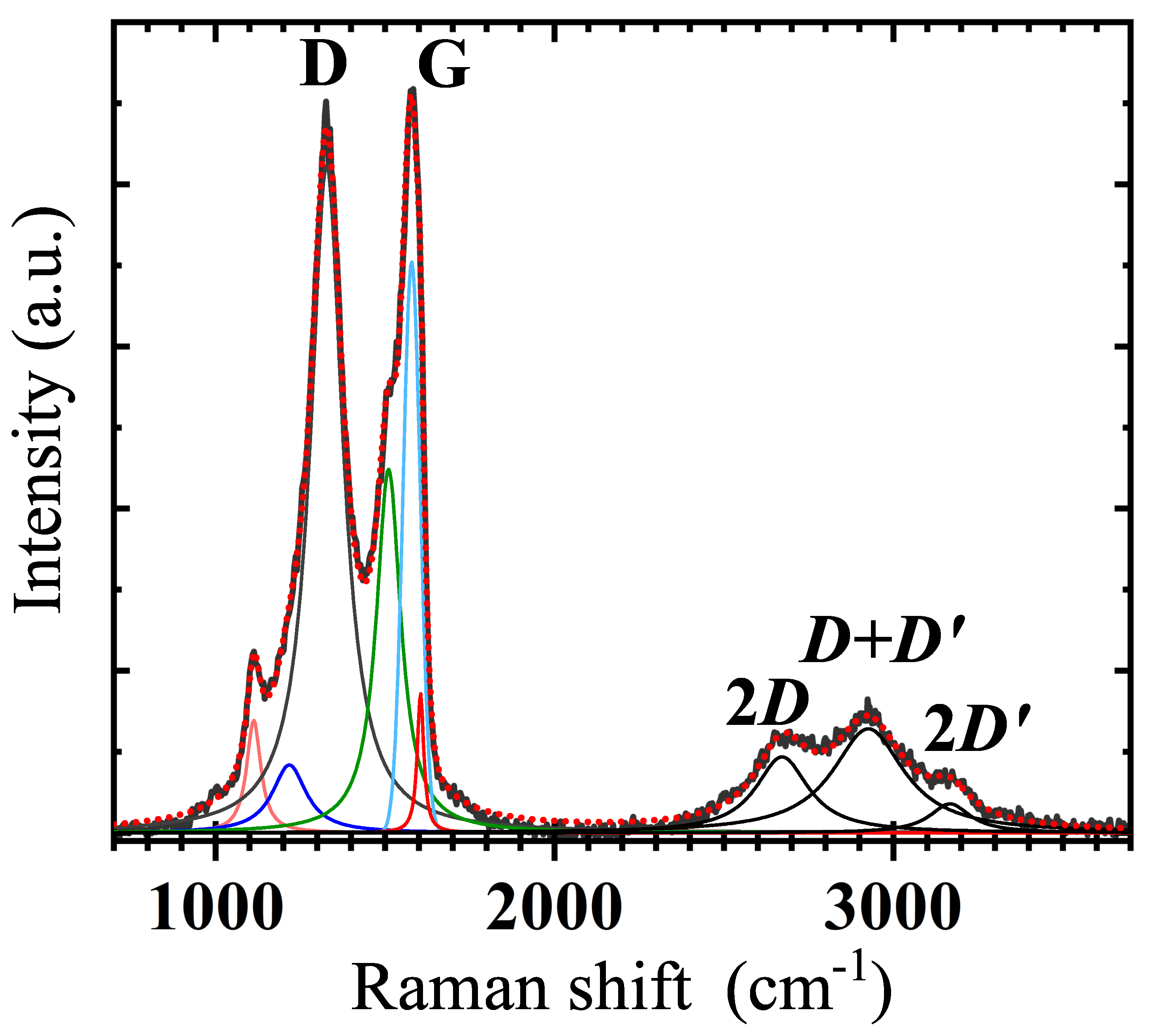
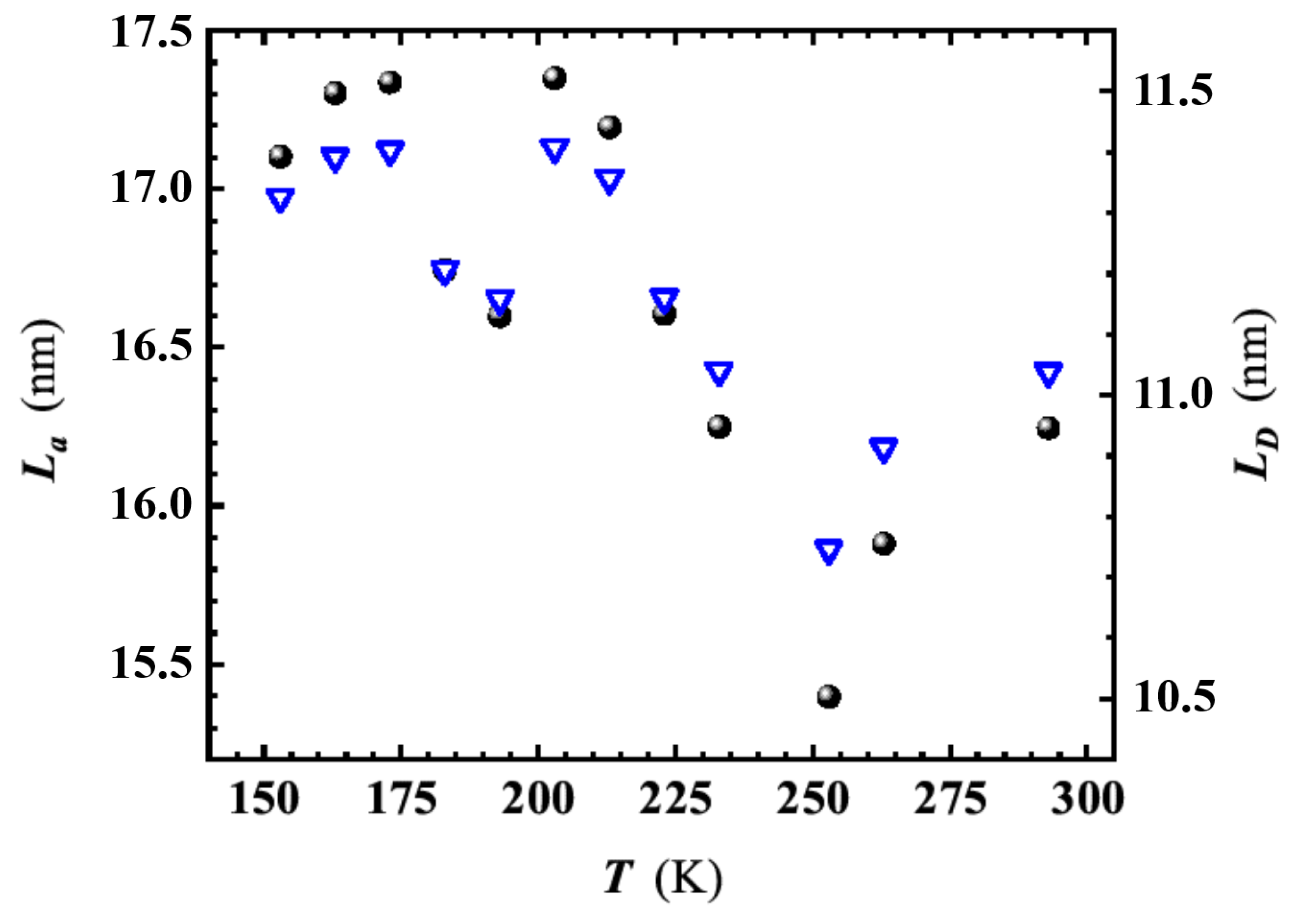
3.2. Raman Spectrum

| Raman Peak/Band | Position (Expected) | FWHM (meas.) | Position (meas.) | Amplitude (meas.) |
|---|---|---|---|---|
| 1100 a | 51 | 1112 | 0.1387 | |
| 1200 b | 122 | 1217 | 0.0837 | |
| D | 1327 c | 116 | 1327 | 0.8233 |
| 1500 d | 88 | 1510 | 0.4480 | |
| G | 1593 e | 60 | 1578 | 0.7042 |
| 1610 f | 23 | 1604 | 0.1726 | |
| 2690 g | 190 | 2671 | 0.0937 | |
| 2925 h | 267 | 2926 | 0.1284 | |
| 3160 i | 145 | 3167 | 0.0358 |
3.3. Temperature Dependence
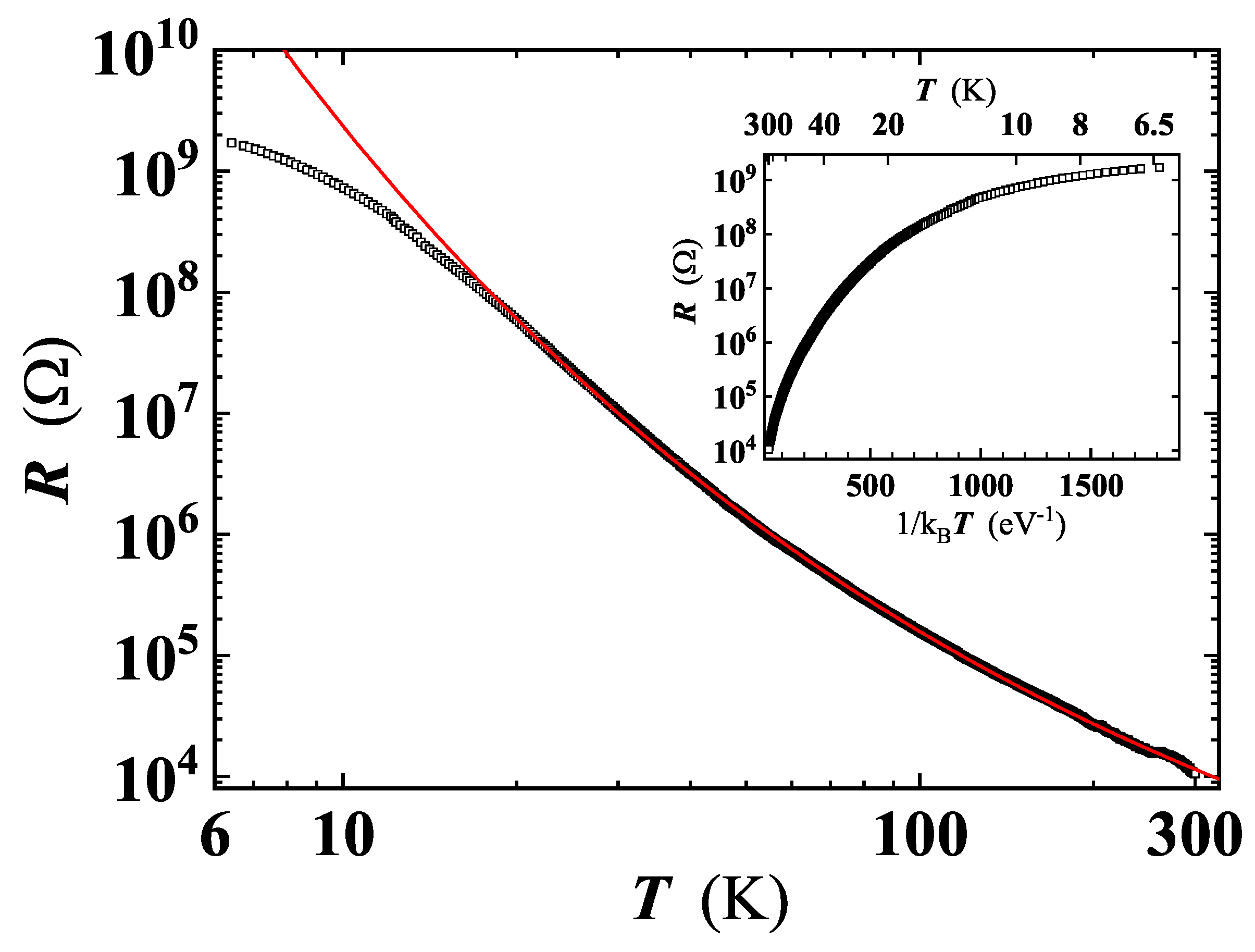
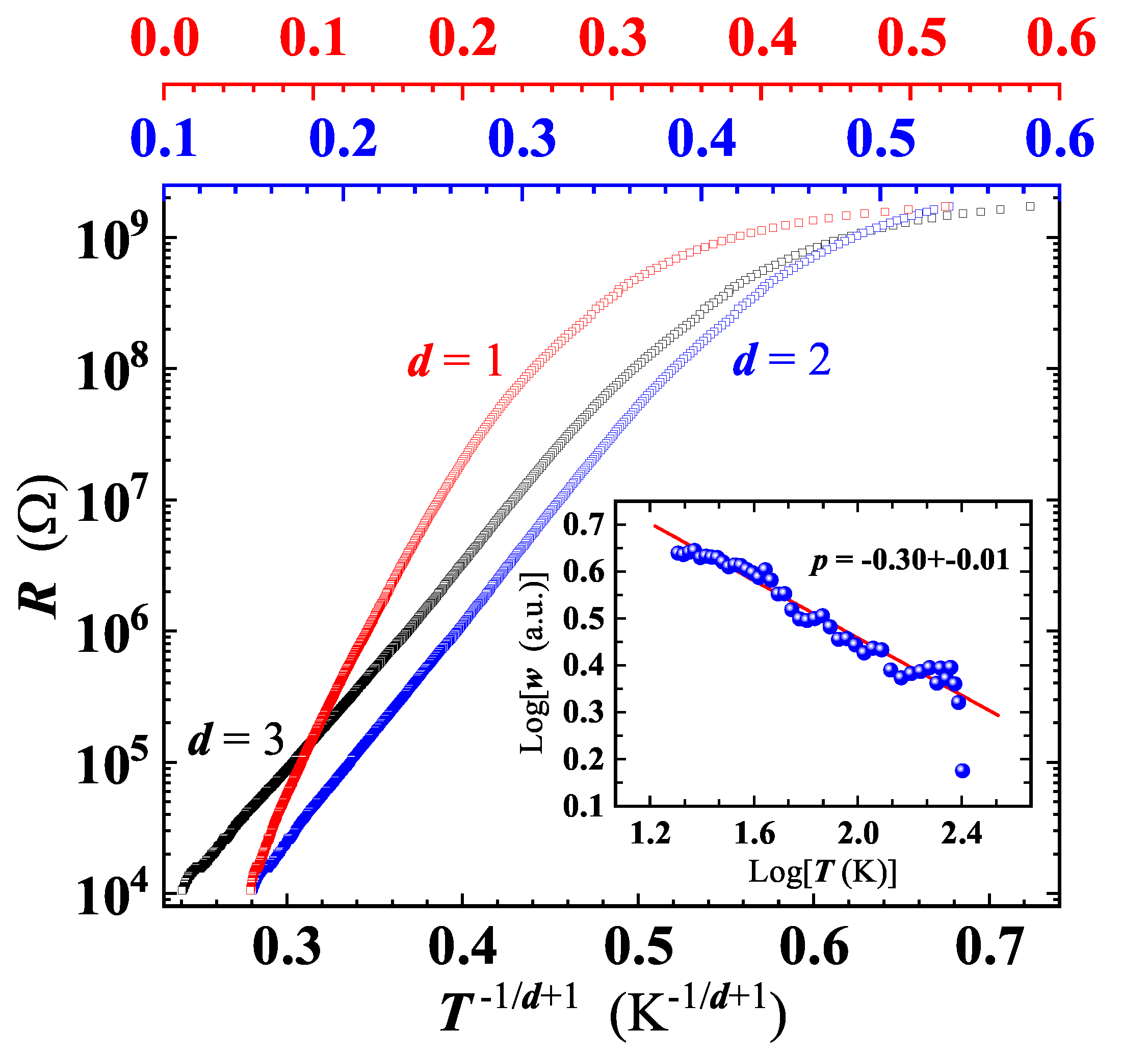
3.4. Transport Properties
4. Discussion
5. Conclusions
6. Additional Information
Author Contributions
Funding
Data Availability Statement
Acknowledgments
Conflicts of Interest
References
- De Nicola, F.; Viola, I.; Tenuzzo, L.D.; Rasch, F.; Lohe, M.R.; Nia, A.S.; Schütt, F.; Feng, X.; Adelung, R.; Lupi, S. Wetting Properties of Graphene Aerogels. Sci. Rep. 2020, 10, 1916. [Google Scholar] [CrossRef]
- Chabot, V.; Higgins, D.; Yu, A.; Xiao, X.; Chen, Z.; Zhang, J. A review of graphene and graphene oxide sponge: Material synthesis and applications to energy and the environment. Energy Environ. Sci. 2014, 7, 1564–1596. [Google Scholar] [CrossRef]
- Christian, M.; Mazzaro, R.; Morandi, V. Bioinspired Design of Graphene-Based Materials. Adv. Funct. Mater. 2020, 30, 2007458. [Google Scholar] [CrossRef]
- Kim, B.J.; Yang, G.; Park, M.J.; Kwak, J.S.; Baik, K.H.; Kim, D.; Kim, J. Three-dimensional graphene foam-based transparent conductive electrodes in GaN-based blue light-emitting diodes. Appl. Phys. Lett. 2013, 102, 1619022. [Google Scholar] [CrossRef]
- Wei, J.; Zang, Z.; Zhang, Y.; Wang, M.; Du, J.; Tang, X. Enhanced performance of light-controlled conductive switching in hybrid cuprous oxide/reduced graphene oxide (Cu2O/rGO) nanocomposites. Opt. Lett. 2017, 42, 911–914. [Google Scholar] [CrossRef] [PubMed]
- Ma, Y.; Chen, Y. Three-dimensional graphene networks: Synthesis, properties and applications. Nat. Sci. Rev. 2015, 2, 40–53. [Google Scholar] [CrossRef] [Green Version]
- Biener, J.; Stadermann, M.; Suss, M.; Worsley, M.A.; Biener, M.; Rose, K.A.; Baumann, T.F. Advanced carbon aerogels for energy applications. Energy Environ. Sci. 2011, 4, 656–667. [Google Scholar] [CrossRef]
- Chen, W.; Huang, Y.X.; Li, D.B.; Yu, H.Q.; Yan, L. Preparation of a macroporous flexible three dimensional graphene sponge using an ice-template as the anode material for microbial fuel cells. Res. Adv. 2014, 4, 21619–21624. [Google Scholar] [CrossRef]
- Luo, J.; Liu, J.; Zeng, Z.; Ng, C.F.; Ma, L.; Zhang, H.; Lin, J.; Shen, Z.; Fan, H.J. Three-dimensional graphene foam supported Fe3O4 lithium battery anodes with long cycle life and high rate capability. Nano Lett. 2013, 13, 6136–6143. [Google Scholar] [CrossRef]
- Cao, X.; Yin, Z.; Zhang, H. Three-dimensional graphene materials: Preparation, structures and application in supercapacitors. Energy Environ. Sci. 2014, 7, 1850–1865. [Google Scholar] [CrossRef] [Green Version]
- Ye, S.; Feng, J. Self-assembled three-dimensional hierarchical graphene/polypyrrole nanotube hybrid aerogel and its application for supercapacitors. ACS Appl. Mat. Interf. 2014, 6, 9671–9679. [Google Scholar] [CrossRef]
- Bi, H.; Huang, F.; Liang, J.; Tang, Y.; Lu, X.; Xie, X.; Jiang, M. Large-scale preparation of highly conductive three dimensional graphene and its applications in CdTe solar cells. J. Mat. Chem. 2011, 21, 17366–17370. [Google Scholar] [CrossRef]
- Park, J.J.; Lee, M.; Kim, Y.; Kim, D.Y. Nonpolar Solvent-Dispersible Alkylated Reduced Graphene Oxide for Hole Transport Material in n-i-p Perovskite Solar Cells. Sol. RRL 2021, 5, 2100087. [Google Scholar] [CrossRef]
- Giorgianni, F.; Vicario, C.; Shalaby, M.; Tenuzzo, L.D.; Marcelli, A.; Zhang, T.; Zhao, K.; Chen, Y.; Hauri, C.; Lupi, S. High-Efficiency and Low Distortion Photoacoustic Effect in 3D Graphene Sponge. Adv. Func. Mat. 2018, 28, 1702652. [Google Scholar] [CrossRef] [Green Version]
- De Nicola, F.; Tenuzzo, L.D.; Viola, I.; Zhang, R.; Zhu, H.; Marcelli, A.; Lupi, S. Ultimate Photo-Thermo-Acoustic Efficiency of Graphene Aerogels. Sci. Rep. 2019, 9, 1–6. [Google Scholar]
- Bagoole, O.; Rahman, M.; Younes, H.; Shah, S.; Al Ghaferi, A. Three-dimensional graphene interconnected structure, fabrication methods and applications: Review. J. Nanomed. Nanotechnol. 2017, 8, 2. [Google Scholar]
- Li, J.; Zhao, S.; Zhang, G.; Gao, Y.; Deng, L.; Sun, R.; Wong, C.P. A facile method to prepare highly compressible three-dimensional graphene-only sponge. J. Mater. Chem. A 2015, 3, 15482–15488. [Google Scholar] [CrossRef]
- Banciu, C.; Lungulescu, M.; Băra, A.; Leonat, L.; Teișanu, A. 3D graphene network investigation by Raman spectroscopy. Optoelectron. Adv. Mater.-Rapid Commun. 2017, 11, 368–372. [Google Scholar]
- Stankovich, S.; Dikin, D.A.; Piner, R.D.; Kohlhaas, K.A.; Kleinhammes, A.; Jia, Y.; Wu, Y.; Nguyen, S.T.; Ruoff, R.S. Synthesis of graphene-based nanosheets via chemical reduction of exfoliated graphite oxide. Carbon 2007, 45, 1558–1565. [Google Scholar] [CrossRef]
- Zhang, S.; Jiang, S.F.; Huang, B.C.; Shen, X.C.; Chen, W.J.; Zhou, T.P.; Cheng, H.Y.; Cheng, B.H.; Wu, C.Z.; Li, W.W.; et al. Sustainable production of value-added carbon nanomaterials from biomass pyrolysis. Nat. Sustain. 2020. [Google Scholar] [CrossRef]
- Wojdyr, M. Fityk: A general-purpose peak fitting program. J. Appl. Crystallogr. 2010, 43, 1126–1128. [Google Scholar] [CrossRef]
- Ferrari, A.C.; Robertson, J. Interpretation of Raman spectra of disordered and amorphous carbon. Phys. Rev. B 2000, 61, 14095–14107. [Google Scholar] [CrossRef] [Green Version]
- Pinto, N.; Rezvani, S.J.; Perali, A.; Flammia, L.; Milošević, M.V.; Fretto, M.; Cassiago, C.; De Leo, N. Dimensional crossover and incipient quantum size effects in superconducting niobium nanofilms. Sci. Rep. 2018, 8, 4710. [Google Scholar] [CrossRef] [PubMed] [Green Version]
- Rezvani, S.J.; Perali, A.; Fretto, M.; De Leo, N.; Flammia, L.; Milošević, M.; Nannarone, S.; Pinto, N. Substrate-Induced Proximity Effect in Superconducting Niobium Nanofilms. Condens. Matter 2019, 4, 4. [Google Scholar] [CrossRef] [Green Version]
- Kaniyoor, A.; Ramaprabhu, S. A Raman spectroscopic investigation of graphite oxide derived graphene. Aip Adv. 2012, 2, 032183. [Google Scholar] [CrossRef] [Green Version]
- Muzyka, R.; Drewniak, S.; Pustelny, T.; Chrubasik, M.; Gryglewicz, G. Characterization of graphite oxide and reduced graphene oxide obtained from different graphite precursors and oxidized by different methods using Raman spectroscopy. Materials 2018, 11, 1050. [Google Scholar] [CrossRef] [PubMed] [Green Version]
- Jorio, A.; Saito, R.; Dresselhaus, G.; Dresselhaus, M.S. Raman Spectroscopy: From Graphite to sp2 Nanocarbons. In Raman Spectroscopy in Graphene Related Systems; John Wiley & Sons, Ltd.: Hoboken, NJ, USA, 2011; Chapter 4; pp. 73–101. [Google Scholar] [CrossRef]
- Cheruku, R.; Bhaskaram, D.S.; Govindaraj, G. Variable range hopping and relaxation mechanism in graphene oxide sheets containing sp3 hybridization induced localization. J. Mater. Sci. Mater. Electron. 2018, 29, 9663–9672. [Google Scholar] [CrossRef]
- Ferrari, A.C.; Basko, D.M. Raman spectroscopy as a versatile tool for studying the properties of graphene. Nat. Nanotech. 2013, 8, 235. [Google Scholar] [CrossRef] [Green Version]
- Thomsen, C.; Reich, S. Double Resonant Raman Scattering in Graphite. Phys. Rev. Lett. 2000, 85, 5214. [Google Scholar] [CrossRef]
- Chen, J.; Cullen, W.G.; Jang, C.; Fuhrer, M.S.; Williams, E.D. Defect scattering in graphene. Phys. Rev. Lett. 2009, 102, 236805. [Google Scholar] [CrossRef]
- Narula, R.; Reich, S. Double resonant Raman spectra in graphene and graphite: A two-dimensional explanation of the Raman amplitude. Phys. Rev. B 2008, 78, 165422. [Google Scholar] [CrossRef] [Green Version]
- Paillard, V. On the origin of the 1100 cm-1 Raman band in amorphous and nanocrystalline sp3 carbon. Europhys. Lett. 2001, 54, 194–198. [Google Scholar] [CrossRef]
- Ferrari, A.; Robertson, J. Origin of the 1150 cm-1 Raman mode in nanocrystalline diamond. Phys. Rev. B 2001, 63, 121405. [Google Scholar] [CrossRef]
- Ferrari, A.C.; Meyer, J.; Scardaci, V.; Casiraghi, C.; Lazzeri, M.; Mauri, F.; Piscanec, S.; Jiang, D.; Novoselov, K.; Roth, S.; et al. Raman spectrum of graphene and graphene layers. Phys. Rev. Lett. 2006, 97, 187401. [Google Scholar] [CrossRef] [PubMed] [Green Version]
- Cançado, L.G.; Jorio, A.; Ferreira, E.M.; Stavale, F.; Achete, C.A.; Capaz, R.B.; Moutinho, M.V.O.; Lombardo, A.; Kulmala, T.S.; Ferrari, A.C. Quantifying defects in graphene via Raman spectroscopy at different excitation energies. Nano Lett. 2011, 11, 3190–3196. [Google Scholar] [CrossRef] [PubMed] [Green Version]
- Cançado, L.G.; Takai, K.; Enoki, T.; Endo, M.; Kim, Y.A.; Mizusaki, H.; Jorio, A.; Coelho, L.N.; Magalhaes-Paniago, R.; Pimenta, M.A. General equation for the determination of the crystallite size La of nanographite by Raman spectroscopy. Appl. Phys. Lett. 2006, 88, 163106. [Google Scholar] [CrossRef]
- Gómez-Navarro, C.; Weitz, R.T.; Bittner, A.M.; Scolari, M.; Mews, A.; Burghard, M.; Kern, K. Electronic Transport Properties of Individual Chemically Reduced Graphene Oxide Sheets. Nano Lett. 2007, 7, 3499–3503. [Google Scholar] [CrossRef]
- Bhaskaram, D.S.; Govindaraj, G. Carrier Transport in Reduced Graphene Oxide Probed Using Raman Spectroscopy. J. Phys. Chem. C 2018, 122, 10303–10308. [Google Scholar] [CrossRef]
- Eda, G.; Mattevi, C.; Yamaguchi, H.; Kim, H.; Chhowalla, M. Insulator to Semimetal Transition in Graphene Oxide. J. Phys. Chem. C 2009, 113, 15768. [Google Scholar] [CrossRef] [Green Version]
- Joung, D.; Khondaker, S.I. Efros-Shklovskii variable-range hopping in reduced graphene oxide sheets of varying carbon sp2 fraction. Phys. Rev. B 2012, 86, 235423. [Google Scholar] [CrossRef] [Green Version]
- Wu, X.; Sprinkle, M.; Li, X.; Ming, F.; Berger, C.; de Heer, W. Epitaxial-graphene/graphene-oxide junction: An essential step towards epitaxial graphene electronics. Physics. Rev. Lett. 2008, 101, 026801. [Google Scholar] [CrossRef] [PubMed] [Green Version]
- Gierz, I.; Riedl, C.; Starke, U.; Ast, C.; Kern, K. Atomic hole doping of graphene. Nano Lett. 2008, 8, 4603–4607. [Google Scholar] [CrossRef] [PubMed] [Green Version]
- Kim, H.J.; Kim, D.; Jung, S.; Yi, S.N.; Yun, Y.J.; Chang, S.; Ha, D. Charge Transport in Thick Reduced Graphene Oxide Film. J. Phys. Chem. C 2015, 119, 28685–28690. [Google Scholar] [CrossRef]
- Rezvani, S.; D’Elia, A.; Macis, S.; Nannarone, S.; Lupi, S.; Schutt, F.; Rasch, F.; Adelung, R.; Lu, B.; Zhang, Z.; et al. Structural anisotropy in three dimensional macroporous graphene: A polarized XANES investigation. Diam. Relat. Mater. 2021, 111, 108171. [Google Scholar] [CrossRef]
- Baek, S.J.; Hong, W.G.; Park, M.; Kaiser, A.; Kim, H.J.; Kim, B.H.; Park, Y.W. The Effect of Oxygen Functional Groups on the Electrical Transport Behavior of a Single Piece Multi-layered Graphene Oxide. Synth. Met. 2014, 191, 1–5. [Google Scholar] [CrossRef]
- Kaiser, A.B.; Gómez-Navarro, C.; Sundaram, R.S.; Burghard, M.; Kern, K. Electrical Conduction Mechanism in Chemically Derived Graphene Monolayers. Nano Lett. 2009, 9, 1787. [Google Scholar] [CrossRef]
- Osofsky, M.S.; Hernández, S.C.; Nath, A.; Wheeler, V.D.; Walton, S.G.; Krowne, C.M.; Gaskill, D.K. Functionalized graphene as a model system for the two-dimensional metal-insulator transition. Sci. Rep. 2016, 6, 19939. [Google Scholar] [CrossRef] [Green Version]
- Wei, G.; Yu, J.; Gu, M.; Tang, T.B. Dielectric relaxation and hopping conduction in reduced graphite oxide. J. Appl. Phys. 2016, 119, 224102. [Google Scholar] [CrossRef]
- Wang, S.T.; Lin, Y.F.; Li, Y.C.; Yeh, P.C.; Tang, S.J.; Rosenstein, B.; Hsu, T.H.; Zhou, X.; Liu, Z.; Lin, M.T.; et al. Direct probing of density of states of reduced graphene oxides in a wide voltage range by tunneling junction. Appl. Phys. Lett. 2012, 101, 183110. [Google Scholar] [CrossRef] [Green Version]
- Pinto, N.; Rezvani, S.J.; Favre, L.; Berbezier, I.; Fretto, M.; Boarino, L. Geometrically induced electron-electron interaction in semiconductor nanowires. Appl. Phys. Lett. 2016, 109, 123101. [Google Scholar] [CrossRef]
- Rezvani, S.J.; Pinto, N.; Enrico, E.; D’Ortenzi, L.; Chiodoni, A.; Boarino, L. Thermally activated tunneling in porous silicon nanowires with embedded Si quantum dots. J. Phys. D Appl. Phys. 2016, 49, 105104. [Google Scholar] [CrossRef]
- Mattevi, C.; Eda, G.; Agnoli, S.; Miller, S.; Mkhoyan, K.; Celik, O.; Mastrogiovanni, D.; Granozzi, G.; Garfunkel, E.; Chhowalla, M. Evolution of electrical, chemical, and structural properties of transparent and conducting chemically derived graphene thin films. Adv. Funct. Mater. 2009, 19, 2577–2583. [Google Scholar] [CrossRef]
- Lahaye, R.J.W.E.; Jeong, H.K.; Park, C.Y.; Lee, Y.H. Density functional theory study of graphite oxide for different oxidation levels. Phys. Rev. B 2009, 79, 125435. [Google Scholar] [CrossRef]
- Bansal, T.; Mohite, A.D.; Shah, H.M.; Galande, C.; Srivastava, A.; Jasinski, J.B.; Ajayan, P.M.; Alphenaar, B.W. New insights into the density of states of graphene oxide using capacitive photocurrent spectroscopy. Carbon 2012, 50, 808–814. [Google Scholar] [CrossRef]
- Zhang, B.; Yang, L.; Li, C.; Hu, B.; Li, Q.; Zheng, C.; Xia, H.; Jin, L. Electrochemical Visualization of Defect-induced Density of States at Single Graphene Flake. J. Electrochem. Soc. 2019, 166, 15. [Google Scholar] [CrossRef]
- Kajen, R.S.; Chandrasekhar, N.; Pey, K.L.; Vijila, C.; Jaiswal, M.; Saravanan, S.; Ng, A.M.H.; Wong, C.P.; Loh, K.P. Charge transport in lightly reduced graphene oxide: A transport energy perspective. J. Appl. Phys. 2013, 113, 063710. [Google Scholar] [CrossRef]


| Element | Atomic No. | Mass Norm. [%] | Atom [%] | Rel. Error [%] () |
|---|---|---|---|---|
| Carbon | 6 | 89.72 | 92.15 | 11.15 |
| Nitrogen | 7 | 0.73 | 0.64 | 36.85 |
| Oxygen | 8 | 9.14 | 7.05 | 15.01 |
| Sulfur | 16 | 0.41 | 0.16 | 16.26 |
Publisher’s Note: MDPI stays neutral with regard to jurisdictional claims in published maps and institutional affiliations. |
© 2021 by the authors. Licensee MDPI, Basel, Switzerland. This article is an open access article distributed under the terms and conditions of the Creative Commons Attribution (CC BY) license (https://creativecommons.org/licenses/by/4.0/).
Share and Cite
Pinto, N.; McNaughton, B.; Minicucci, M.; Milošević, M.V.; Perali, A. Electronic Transport Mechanisms Correlated to Structural Properties of a Reduced Graphene Oxide Sponge. Nanomaterials 2021, 11, 2503. https://doi.org/10.3390/nano11102503
Pinto N, McNaughton B, Minicucci M, Milošević MV, Perali A. Electronic Transport Mechanisms Correlated to Structural Properties of a Reduced Graphene Oxide Sponge. Nanomaterials. 2021; 11(10):2503. https://doi.org/10.3390/nano11102503
Chicago/Turabian StylePinto, Nicola, Benjamin McNaughton, Marco Minicucci, Milorad V. Milošević, and Andrea Perali. 2021. "Electronic Transport Mechanisms Correlated to Structural Properties of a Reduced Graphene Oxide Sponge" Nanomaterials 11, no. 10: 2503. https://doi.org/10.3390/nano11102503
APA StylePinto, N., McNaughton, B., Minicucci, M., Milošević, M. V., & Perali, A. (2021). Electronic Transport Mechanisms Correlated to Structural Properties of a Reduced Graphene Oxide Sponge. Nanomaterials, 11(10), 2503. https://doi.org/10.3390/nano11102503