Abstract
In this paper, a single-stage step-down power factor corrector without a full-bridge rectifier is developed, which is designed to operate in discontinuous conduction mode (DCM). In terms of control, the DCM has the advantages of simple control and easy realization, no slope compensation, zero current switching, and no diode reverse current. By sampling the output voltage and using the voltage-follower control to generate the necessary control force to drive the power switch, not only can the output voltage be stabilized at the desired value, but also the input current can be, as much as possible, in the form of a sinusoidal waveform and can follow the phase of the input voltage. Moreover, the harmonic distortion meets the requirements of the IEC6100-3-2 Class D harmonics standard, and, thus, the proposed rectifier is appropriate for the computer, computer monitor, and television receiver. Eventually, by means of mathematical deductions, simulations by PSIM version 9.1, and experimental results, the feasibility and effectiveness of the proposed circuit can be verified.
1. Introduction
Thanks to the rapid development of technology and power electronics, low-frequency harmonic currents created by the characteristics of nonlinear loads of power electronics products flow into the power system in large quantities, thereby leading to increasingly serious harmonic pollution of the power system. As generally acknowledged, the harmonic current will change the output voltage waveform of the power system. When the harmonic current generated is larger or exceeds the permissible value, it may cause other products in its vicinity to operate incorrectly, measurement errors, efficiency degradation, or even burnout. Therefore, harmonics are regulated in various countries around the world. The International Electrotechnical Commission (IEC) in Europe has issued the IEC61000-3-2 harmonic standard [1], and Japanese specifications have also been issued, JIS-C-C. The Japanese authority also promulgated the JIS-C-61000-3-2 standard [2], which formally regulates the harmonics generated by electronic equipment products, and stipulates that all electronic equipment products with an output power of 75 W or more must pass a harmonics test.
In order to improve harmonic and power-factor problems, it is necessary to add a power factor correction (PFC) circuit. The main function of this circuit is to make the input voltage and input current in the same phase, so that the load observed by the utility is similar to the resistive load. They can be categorized into passive and active power factor correction circuits, depending on the components used.
Passive power factor correctors [3] are composed of passive components, including inductors, capacitors, diodes, etc. These circuits have the advantages of a simple circuit structure, low cost, and low electromagnetic interference, etc. However, they are bulky, heavy, inefficient, and lack flexibility in the circuits. That is to say, the passive power factor correction is ineffective, and they are not suitable for today’s stringent power factor requirements.
Due to the above disadvantages of passive PFC rectifiers, active PFC rectifiers were developed. Generally, the circuit components of the active PFC rectifier [4] include switching switches, inductors, and diodes, etc. According to the input conditions and output load requirements, the timing of the main power switch can be controlled by appropriate feedback compensation control and pulse width modulation (PWM) to make the phase of the input current closely follow the phase of the input voltage, so as to stabilize the output voltage, as well as to control the input current waveform to meet the harmonic specification.
Commonly used single-stage active power PFC rectifiers are classified into two types, boost-derived and buck-derived, among which the boost PFC circuits have been widely used [5,6,7,8,9,10,11,12,13,14,15,16,17,18]. The boost PFC rectifier has the following advantages: (i) the inductor is directly connected to the power supply at the input end, and in the continuous conduction mode (CCM), the input current is continuous; so that the input current spike can be suppressed, the electromagnetic interference is smaller, and the power factor can be higher; (ii) the main power switch driver does not need to be isolated, so that the driver circuit is easy to design; (iii) the input current is the inductor current, which makes it easy to realize current mode control; (iv) it has a high output voltage, so compared to other circuit topologies, it has a better hold-up time after a power failure when using the same capacitor size. However, because of the higher output voltage, there are some drawbacks: (i) the voltage tolerance of the power switch has to be large enough; (ii) to meet the demand of the back-end load voltage, an additional regulation stage or isolation step-down circuit is required, thereby increasing the cost; and (iii) the high output voltage is prone to causing a high common-mode noise.
The studies [19,20,21,22,23,24,25,26,27,28,29,30,31] present buck PFC rectifiers, which can convert a higher input AC voltage into a lower DC voltage. The advantage of this circuit is that the voltage stress of the power switch is the maximum value of the input voltage, and compared with the boost PFC rectifier, the power switch can be selected with a smaller withstand voltage, and thus the cost is cheaper. However, there is no input current when the input voltage is lower than the output voltage, resulting in zero-crossing distortion. Consequently, the input current does not follow the phase of the input voltage at this time, so the power factor is relatively low, as shown in Figure 1. In addition, the switch is floating, which makes it complicated to drive.
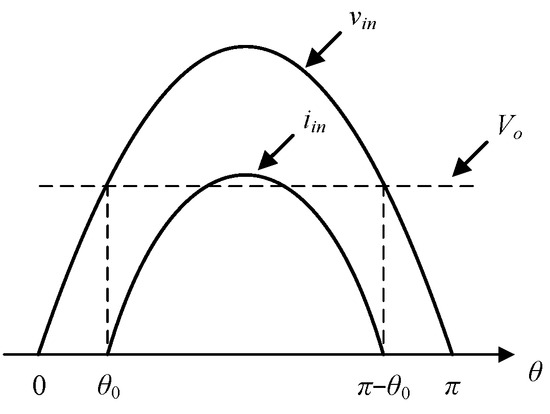
Figure 1.
Input voltage and input current of the buck active PFC rectifier.
The studies [32,33,34] propose buck–boost rectifiers, which have the advantage of being able to step up and step down the input voltage in CCM, thereby providing a wide output voltage range and being easy to design according to the requirements of the back-end circuits. However, the voltage stress of the switch and output diode is the sum of the input voltage and the output voltage. Consequently, the use of components with higher withstand voltages is required. In addition, the switch is floating, which makes it complicated to drive.
In general, traditional active PFC rectifiers are not suitable for high-power applications because when these rectifiers are activated, the full-bridge rectifiers, diodes, and switching elements will have large currents flowing through them, resulting in large conduction losses and switching losses, and hence leading to a reduction in the overall efficiency. In view of this, if the loss of the bridge rectifier can be decreased, the overall efficiency of the circuit can be improved. Therefore, bridgeless active PFC rectifiers are presented [11,12,13,14,15,16,17,18,19,20,21,22,23,24,25,26,27,28,29,30,31,35,36,37,38].
As is generally acknowledged, the PFC control methods can be roughly categorized into the following four types: (1) peak current mode control [7]; (2) average current mode control [8,39]; (3) critical mode control [9,40]; (4) voltage-follower control [36].
For the peak current mode control, if the duty cycle is greater than 50%, the current is prone to sub-harmonic oscillations, so if no proper slope compensation is added to this control, it will result in the distortion of the input current. For the average current control, it makes the transient response of the PFC rectifier slow but is suitable for high-power applications. For the critical mode control, it is difficult to design the filter because it is a variable-frequency control. For the voltage-follower control, due to the high peak current in the power switch when the circuit operates in the discontinuous conduction mode (DCM), it is necessary to select power components with a higher current withstand performance, so it is only suitable for low-power applications.
Accordingly, as shown in Figure 2a, the proposed single-stage step-down power factor corrector without a full-bridge rectifier is presented, which is modified from the existing bridgeless high-PF buck converter [22], as shown in Figure 2b. From these two figures, it can be seen that the former has a lower number of components than the latter.
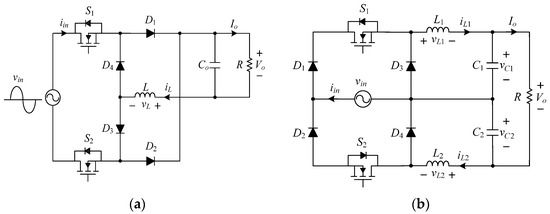
Figure 2.
Single-stage step-down power factor corrector without full-bridge rectifier: (a) the proposed; (b) the existing [22].
Firstly, the system configuration is depicted in Section 2. Sequentially, Section 3 describes the operating principle in detail. After this, the design considerations are given in Section 4. Accordingly, in Section 5, some experimental results are presented to validate the theoretical analysis and designed parameters. Eventually, Section 6 presents a conclusion.
2. System Configuration
Figure 3 displays the system configuration of the proposed rectifier. As for the main power stage, it is constructed by the switches S1 and S2, the diodes D1, D2, D3, and D4, the output inductor L, the output capacitor Co, and the output resistor R. As for the control stage, it is built up by one voltage divider, one analog-to-digital converter (ADC), one gate driver, and one FPGA, which is used to realize voltage-follower control. It is noted that only one gate driving signal is needed to drive the switches S1 and S2. Regarding the control concept, the output voltage is sensed by the voltage divider and sent to the ADC to obtain the corresponding digital signal, which is sent to the FPGA to create suitable gate driving signals to drive the switches S1 and S2, so as to attain the prescribed output voltage, along with a high PF, due to the proposed circuit being operated in DCM. In addition, there is a voltage controller constructed by a proportional-integral (PI) controller and a pulse-width-modulated (PWM) generator inside the FPGA.
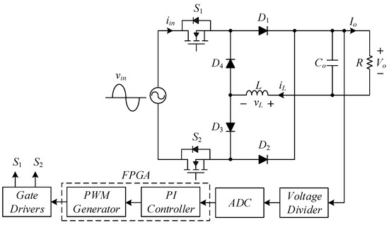
Figure 3.
System configuration.
3. Operating Principle
The operating principle of the proposed single-stage step-down power factor corrector without a full bridge is analyzed, and then the corresponding related theoretical derivation is followed. For analysis convenience, the following assumptions are made first:
- (1)
- All power switches, diodes, inductors, and capacitors are viewed as ideal components.
- (2)
- The value of the output capacitor Co is large enough so that the voltage across Co is stabilized at some output voltage.
- (3)
- The converter is operated in steady state under DCM.
Based on the above assumptions, the illustrated waveforms of the inductor voltage and current in DCM are shown in Figure 4.
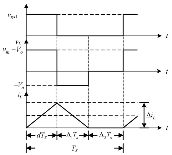
Figure 4.
Illustrated waveforms of inductor voltage and current in DCM in a positive half-cycle.
State 1 : As shown in Figure 5, when the input voltage vin is in a positive half-cycle, the switch S1 is turned on. The input current iin flows through the switch S1, the body diode of the switch S2, the diodes D1 and D3, the output inductor L, and the output capacitor Co. During this state, the voltage across the output inductor L, called vL, is the input voltage vin minus the output voltage Vo, so the output inductor L is in magnetization mode and hence the inductor current iL rises linearly. At the same time, the input power supply charges the output capacitor Co and provides energy to the load R. Moreover, the corresponding time experienced in this state is . In the following, for the first three states, the switch S2 is always off, whereas for the last three states, the switch S1 is always off. As a result, the dead-time effect on switches [41] does not be considered for the proposed rectifier in the actual applications.
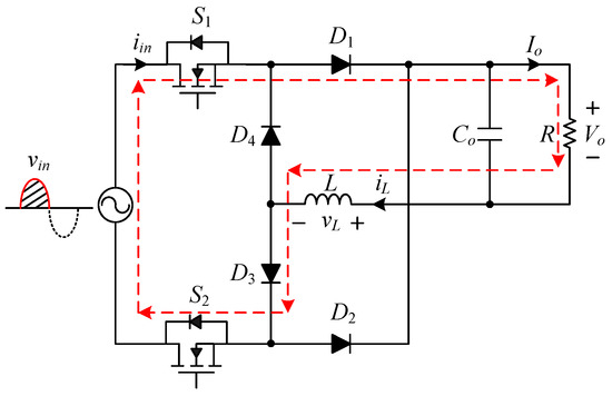
Figure 5.
State 1.
State 2 : As shown in Figure 6, when the input voltage vin is in a positive half-cycle, the switch S1 is cut off, the input current iin is zero, the diodes D1, D2, D3, and D4 conduct, and the inductor current iL continues to flow through these four diodes. During this state, the voltage across the output inductor L is zero minus the output voltage Vo, so the output inductor L is in demagnetization mode and hence the inductor current decreases linearly. At the same time, the output capacitor Co and the output inductor L provide energy to the load R. Moreover, the corresponding time experienced in this state is .
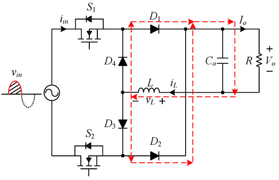
Figure 6.
State 2.
State 3 : As shown in Figure 7, when the input voltage vin is in a positive half-cycle, the switch S1 is still off and the diodes D1, D2, D3, and D4 are all cut off. During this state, there is no current flowing through the inductor L. At the same time, the energy required for the load R is supplied by the output capacitor Co. Moreover, the corresponding time experienced in this state is .
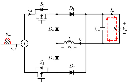
Figure 7.
State 3.
State 4 : As shown in Figure 8, when the input voltage is in a negative half-cycle, the switch S2 is turned on, and the input current iin flows through the switch S2, the body diode of the switch S1, the diodes D2 and D4, the output inductor L, and the output capacitor Co. During this state, the voltage across the output inductor L, called vL, is the input voltage vin minus the output voltage Vo, so the output inductor L is in magnetization mode and hence the inductor current iL rises linearly. At the same time, the input power supply charges the output capacitor Co and provides energy to the load R. Moreover, the corresponding time experienced in this state is .
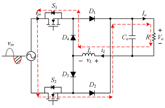
Figure 8.
State 4.
State 5 : When the input voltage is in a negative half-cycle, the switch S2 is cut off, and the behavior is the same as that of state 2, as shown in Figure 6. Moreover, the corresponding time experienced in this state is .
State 6 : When the input voltage is in a negative half-cycle, the switch S2 is still off and diodes D1, D2, D3, and D4 are cut off, and the behavior is the same as that of state 3, as shown in Figure 7. Moreover, the corresponding time experienced in this state is .
Based on the fact that the inductor must obey the volt-second balance, Equation (1) can be obtained as
and
By substituting (2) into (1), the voltage conversion ratio can be calculated as
4. Design Considerations
Table 1 displays the specifications for the proposed rectifier.

Table 1.
System Specifications.
4.1. Design of Output Inductor
In the design of an inductor, it is necessary to consider the peak input AC current when the circuit is operated at the lowest input AC voltage and under the rated output power . By assuming that the input AC voltage and the input AC current are ideal sinusoids, the input AC voltage and the input AC current can be defined as and , respectively, where and are the peak value of the input AC voltage and the peak value of the input AC current, respectively, and is the line radian frequency. To simplify the analysis, the phase angle is replaced by the phase angle , so the input AC voltage can be expressed as follows:
Similarly, the input AC current can be expressed as
As shown in Figure 9, since there is no input current when the input voltage is lower than the output voltage of the buck-type PFC rectifier, it is necessary to assume that the input AC current in (5) should be rewritten into (6).
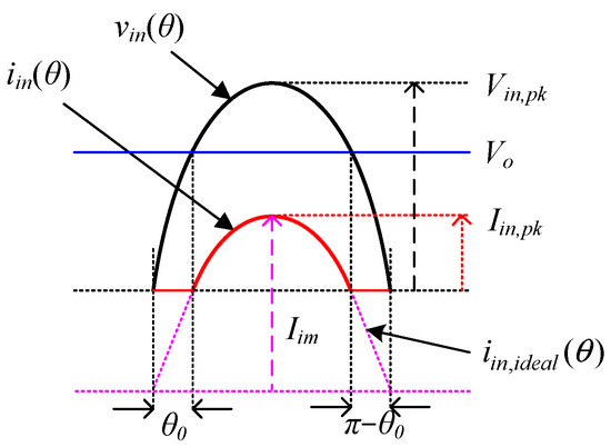 where
is the amplitude of the ideal input AC current .
where
is the amplitude of the ideal input AC current .
Figure 9.
Relationship between input AC voltage and input AC current.
Substituting the system specifications shown in Table 1 and the lowest input AC voltage into (7) yields
By multiplying the instantaneous value of the input AC voltage and the instantaneous value of the input AC current by the time integral, the average input power can be obtained as follows:
Substituting (4) and (6) into (9) yields
The amplitude of the ideal input AC current, called , is determined by the input power Pin, as shown in (11):
In addition, the average input power is obtained from the output power, and the prescribed efficiency, i.e., , (11) can be rewritten as
By substituting the rated output load , the peak value of the minimum input AC voltage , and the results of (8) into (12), the ideal input AC current amplitude can be obtained as follows:
By setting the conduction angle in (7) to , the peak value of the input AC current, called , can be obtained to be
Substituting the results of (8) and (13) into (14) yields
The average value of the inductor current iL, called IL, is
By substituting into (16), the peak value of the average value of the inductor current, called , can be found as
The ripple current through the inductor L can be expressed as
Therefore, if the inductor L is to be operated in the current discontinuous mode (DCM), the value of inductor L must satisfy the following inequality:
Substituting the system specifications shown in Table 1 and the results of (8) and (15) into (19) yields
Accordingly, the MPP powder iron core, manufactured by CSC Co. (Beijing, China) with a model name of CM270125, is used herein and its basic characteristic parameters are shown in Table 2. Therefore, the number of turns can be calculated as below:
Table 2.
Characteristic parameters of powder iron core.
In order to ensure that the required inductance value is sufficient for the converter to operate in DCM under any load condition, the number of turns is taken as 16. Therefore, the actual value of the inductor L is
4.2. Design of Output Capacitor
In the following, the current in the output capacitor Co, called ic(t), can be expressed as
The relationship between the output current capacitor and the output voltage capacitor can be expressed as
By substituting (23) into (24), the output voltage ripple can be expressed as
When the circuit operates in steady state, it can be seen that from (25), the output voltage ripple varies from to and the frequency is twice the utility frequency.
As shown in Table 1, the output voltage ripple is 3% of the output voltage. That is, the peak-to-peak value of the output voltage ripple is
Substituting (27) into (26) yields
Since the step-down power factor corrector has an input voltage lower than the output voltage, it is necessary to multiply the value of by the conduction angle to obtain the value of .
Therefore, a Nippon Chemi-Con electrolytic capacitor connected in parallel with a United Chemi-Con electrolytic capacitor is used as the output capacitor .
5. Experimental Results
The measured waveforms, THD, PF, and efficiency are shown herein.
5.1. Measured Waveforms under 110 V Input Voltage
Figure 10, Figure 11, Figure 12, Figure 13, Figure 14, Figure 15, Figure 16, Figure 17, Figure 18, Figure 19, Figure 20, Figure 21, Figure 22, Figure 23, Figure 24, Figure 25, Figure 26, Figure 27, Figure 28, Figure 29, Figure 30, Figure 31, Figure 32 and Figure 33 show the waveforms at nominal input voltage. Figure 10, Figure 11, Figure 12 and Figure 13 show the waveforms of input AC voltage and input AC current under different output load conditions. From these waveforms, it can be seen that within the range of the conduction angle of the input current, the phase of the input current follows the phase of the input voltage as closely as possible, and the input current is as close as possible to the form of a sinusoidal waveform, so as to achieve the PFC function. From Figure 14, Figure 15, Figure 16 and Figure 17, it can be seen that the harmonics of the input AC current under different output load conditions comply with the harmonic specification of IEC61000-3-2 Class D. For the positive half-cycle of the input voltage, Figure 18, Figure 19, Figure 20 and Figure 21 show the waveforms of vds1 under different output loads. From these waveforms, it can be seen that when the switch S1 is off and the inductor current iL is zero, the waveform of vds1 displays low-frequency oscillation, which is caused by the resonance between the output inductance and the parasitic capacitance of the switch S1. For the negative half-cycle of the input voltage, Figure 22, Figure 23, Figure 24 and Figure 25 show the waveforms of vds2 under different output load conditions. The behavior of the switch S2 is almost identical to that of S1. From Figure 26, Figure 27, Figure 28 and Figure 29, it can be seen that the output inductor current iL is in DCM under different output load conditions, which is consistent with the design requirement. Figure 30, Figure 31, Figure 32 and Figure 33 display the waveforms of the output voltage ripple under different output load conditions. From these waveforms, it can be seen that the output voltage ripple is larger when the output load is heavier.
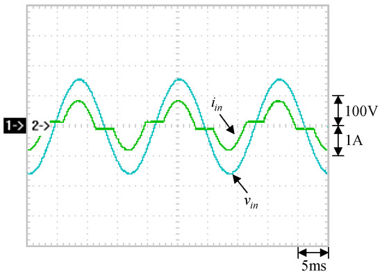
Figure 10.
Measured waveforms under 25% load: (1) vin; (2) iin.
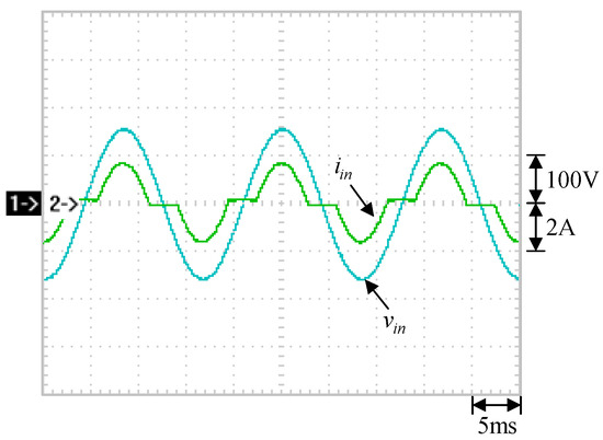
Figure 11.
Measured waveforms under 50% load: (1) vin; (2) iin.
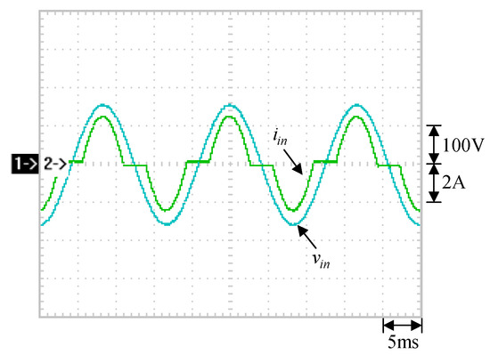
Figure 12.
Measured waveforms under 75% load: (1) vin; (2) iin.
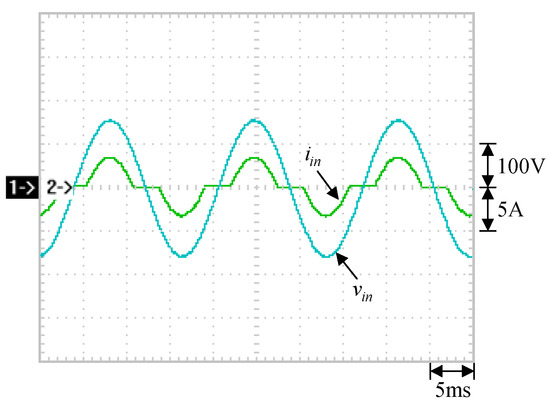
Figure 13.
Measured waveforms under 100% load: (1) vin; (2) iin.
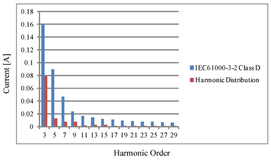
Figure 14.
Harmonic distribution of input current under 25% load [1].
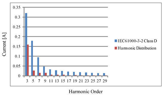
Figure 15.
Harmonic distribution of input current under 50% load [1].
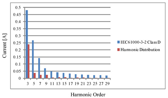
Figure 16.
Harmonic distribution of input current under 75% load [1].
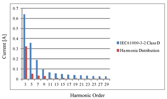
Figure 17.
Harmonic distribution of input current under 100% load [1].
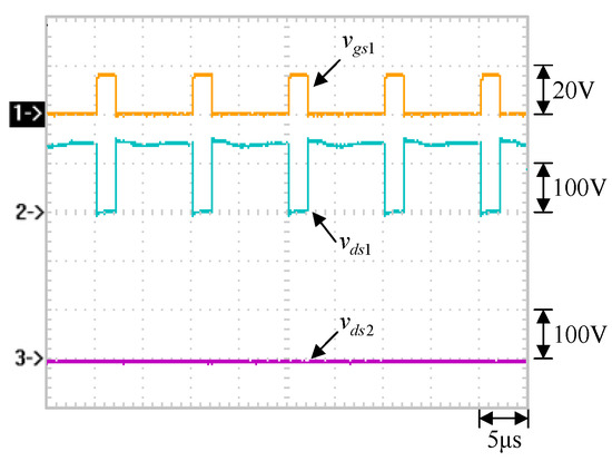
Figure 18.
Measured waveforms at the peak of the positive half-cycle under 25% load: (1) vgs1; (2) vds1; (3) vds2.
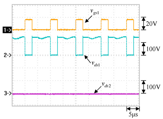
Figure 19.
Measured waveforms at the peak of the positive half-cycle under 50% load: (1) vgs1; (2) vds1; (3) vds2.
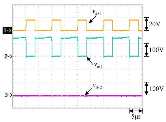
Figure 20.
Measured waveforms at the peak of the positive half-cycle under 75% load: (1) vgs1; (2) vds1; (3) vds2.
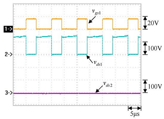
Figure 21.
Measured waveforms at the peak of the positive half-cycle under 100% load: (1) vgs1; (2) vds1; (3) vds2.
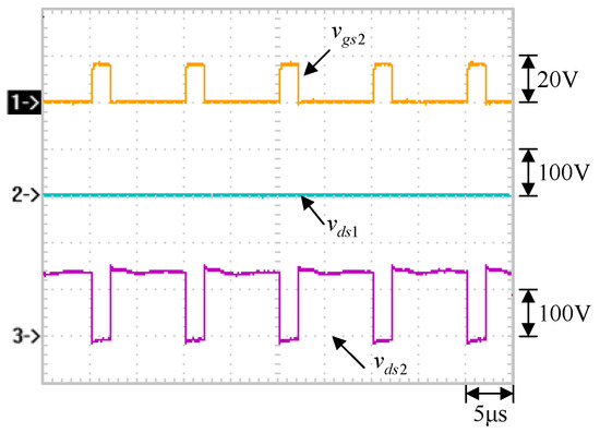
Figure 22.
Measured waveforms at the valley of the negative half-cycle under 25% load: (1) vgs2; (2) vds1; (3) vds2.

Figure 23.
Measured waveforms at the valley of the negative half-cycle under 50% load: (1) vgs2; (2) vds1; (3) vds2.
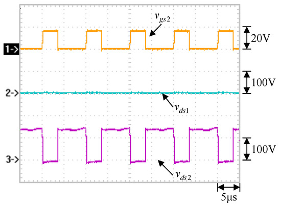
Figure 24.
Measured waveforms at the valley of the negative half-cycle under 75% load: (1) vgs2; (2) vds1; (3) vds2.
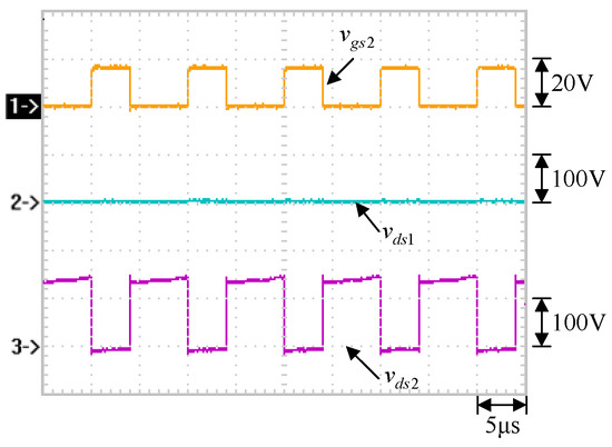
Figure 25.
Measured waveforms at the valley of the negative half-cycle under 100% load: (1) vgs2, (2) vds1, (3) vds2.
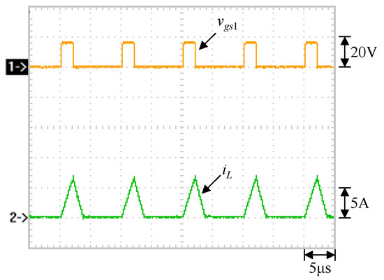
Figure 26.
Measured waveforms at the peak of the positive half-cycle under 25% load: (1) vgs1; (2) iL.
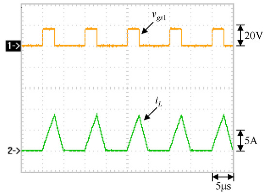
Figure 27.
Measured waveforms at the peak of the positive half-cycle under 50% load: (1) vgs1; (2) iL.
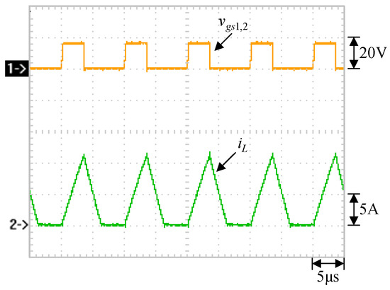
Figure 28.
Measured waveforms at the peak of the positive half-cycle under 75% load: (1) vgs1,2; (2) iL.
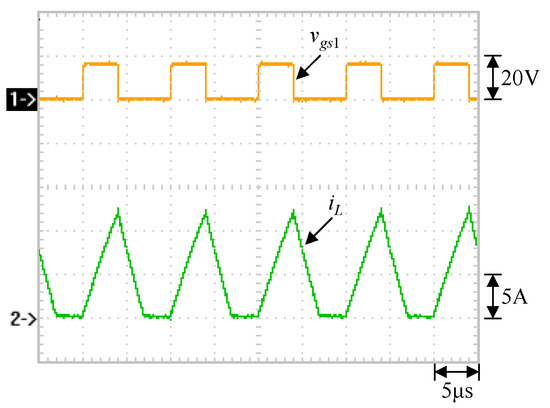
Figure 29.
Measured waveforms at the peak of the positive half-cycle under 100% load: (1) vgs1; (2) iL.

Figure 30.
Output voltage ripple under 25% load.
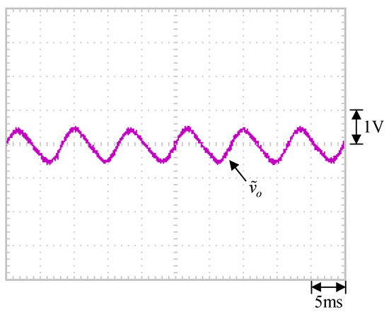
Figure 31.
Output voltage ripple under 50% load.
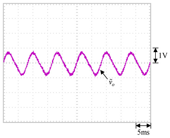
Figure 32.
Output voltage ripple under 75% load.
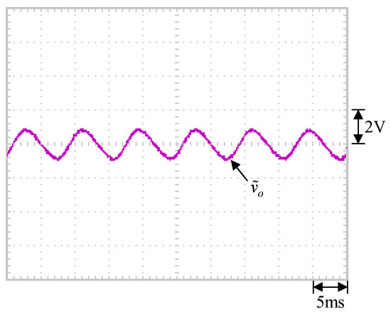
Figure 33.
Output voltage ripple of under 100% load.
5.2. Measured Output Voltage Ripple under 100% Load at Different Input Voltages
Figure 34a–c display the waveforms of the output voltage ripple under an output power of 90 W at input voltages of 90 V, 110 V, and 130 V, respectively. The expression of the output voltage ripple can be seen from (25), and the output voltage ripple is only related to the output current and is independent of the input voltage.
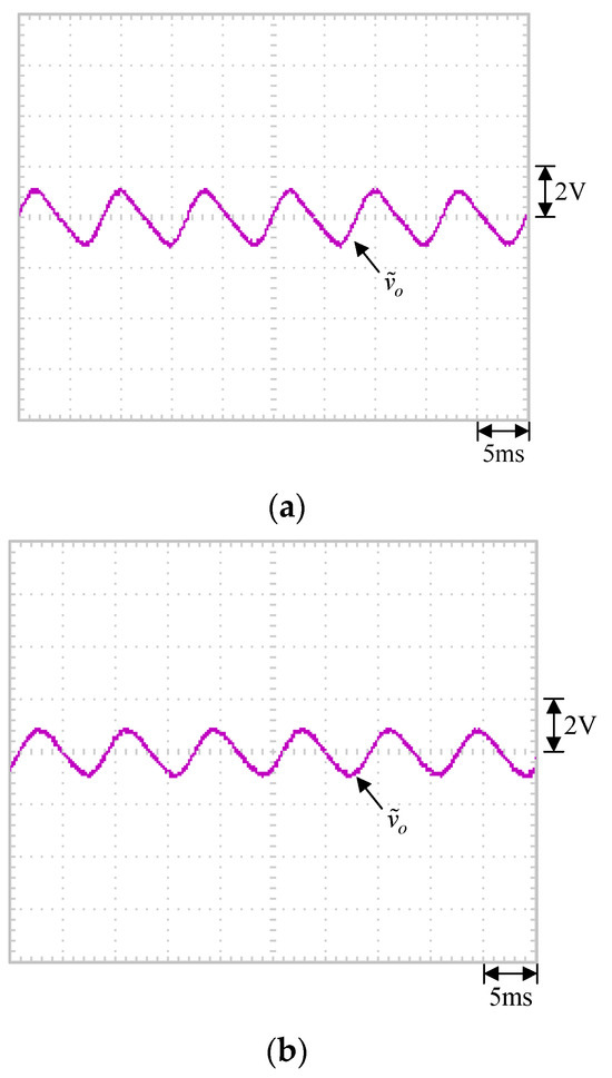
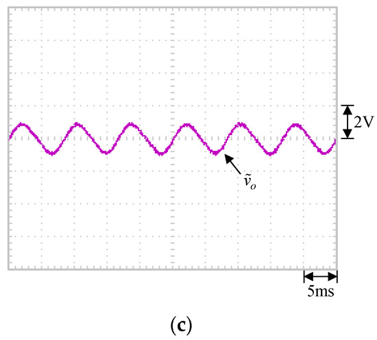
Figure 34.
Output voltage ripple under 100% load at input voltages of (a) 90 V; (b) 110 V; (c) 130 V.
5.3. Measured Curves of THD, PF, and Efficiency
Figure 35 and Figure 36 show the curves of THD and PF versus output power at different input voltages, respectively. From Figure 35, it can be seen that under the same output power, the lower the input voltage, the higher the THD. This is because there is more distortion current created from the lower input voltage. From Figure 36, it can be seen that under the same output power, the lower the input voltage, the lower the PF. This is because there is more difference in phase between the input voltage and the fundamental input current. From this figure, it can be seen that the PF can be kept above 0.88. And, the maximum PF is 0.95. Figure 37 shows the curve of efficiency versus output power at different input voltages. From this figure, it can be seen that the efficiency can be maintained above 95%. And, the maximum efficiency is 96.8% and can be achieved at the lowest input voltage under the minimum output power. In addition, the power losses at load under input voltages of 90 V, 110 V, and 130 V are 4.342 W, 4.064 W, and 3.817 W, respectively.
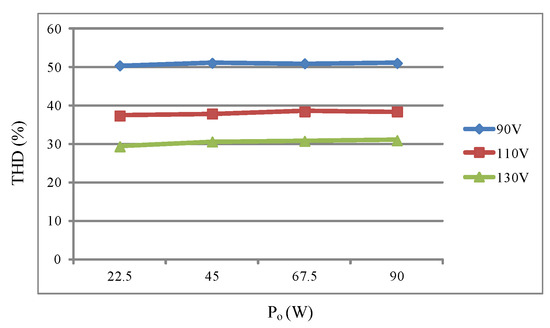
Figure 35.
Curves of THD vs. output power at different input voltages.
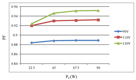
Figure 36.
Curves of PF vs. output power at different input voltages.
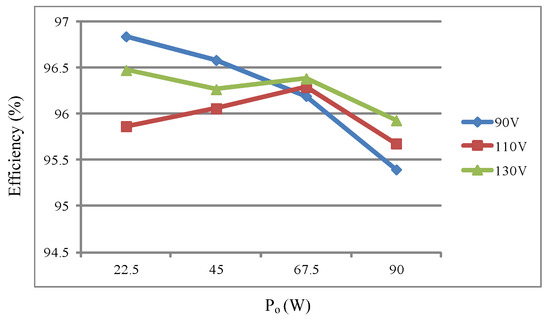
Figure 37.
Curves of efficiency vs. output power at different input voltages.
5.4. Comparison between the Proposed and the Existing
There are many other existing papers investigating bridgeless single-stage step-down PFC [22,23,24,25,26,27,28,29,30,31] circuit structures, which are summarized in Table 3. From Table 3, it can be seen that the proposed circuit has a lower number of output inductors and capacitors as well as the same number of switches, magnetic elements, and diodes, as compared to the existing bridgeless buck PFC circuits.
Table 3.
Comparison of the proposed topology and the existing topologies in [22,23,24,25,26,27,28,29,30,31].
6. Conclusions
A single-stage step-down power factor corrector without a full-bridge rectifier is presented. From the experimental results, it can be seen that the proposed circuit can operate in DCM at different input voltages under output load conditions, which is consistent with the design results. Furthermore, this circuit can pass the IEC61000-3-2 Class D harmonic specification under all experimental conditions. In addition, the maximum PF is 0.95 and the maximum efficiency is 96.8%. As compared with the existing circuits, shown in [22,23,24,25,26,27,28,29,30,31], the proposed circuit has a lower number of output inductors and capacitors as well as the same number of switches and diodes.
Author Contributions
Conceptualization, K.-I.H. and J.-J.S.; methodology, K.-I.H. and J.-J.S.; software, Y.-P.H.; validation, J.-J.S. and Y.-P.H.; formal analysis, Y.-P.H.; investigation, J.-J.S. and Y.-P.H.; resources, K.-I.H.; data curation, J.-J.S. and Y.-P.H.; writing—original draft preparation, K.-I.H.; writing—review and editing, K.-I.H.; visualization, J.-J.S. and Y.-P.H.; supervision, K.-I.H.; project administration, K.-I.H.; funding acquisition, K.-I.H. All authors have read and agreed to the published version of the manuscript.
Funding
This research was funded by the Ministry of Science and Technology, Taiwan, under the grant number: NSTC 112-2221-E-027-015-MY2.
Data Availability Statement
The original contributions presented in the study are included in the article, further inquiries can be directed to the corresponding author.
Conflicts of Interest
The authors declare no conflicts of interest.
References
- IEC61000-3-2; Electromagnetic Compatibility (EMC)-Part 3-2: Limits-Limits for Harmonic Current Emissions (Equipment Input Current ≤ 16 A per Phase). International Electrotechnical Commission: Geneva, Switzerland, 2018.
- JIS-C-61000-3-2; Electromagnetic Compatibility (EMC)-Part 3-2: Limits-Limits for Harmonic Current Emissions (Equipment Input Current ≤ 20 A per Phase). International Electrotechnical Commission: Geneva, Switzerland, 2023.
- Farcas, C.; Petreus, D.; Simion, E.; Palaghita, N.; Juhos, Z. A novel topology based on forward converter with passive power factor correction. In Proceedings of the 2006 29th International Spring Seminar on Electronics Technology, St. Marienthal, Germany, 10–14 May 2006; pp. 268–272. [Google Scholar]
- Umesh, S.; Venkatesha, L.; Usha, A. Active power factor correction technique for single phase full bridge rectifier. In Proceedings of the 2014 International Conference on Advances in Energy Conversion Technologies (ICAECT), Manipal, India, 23–25 January 2014; pp. 130–135. [Google Scholar]
- Zhang, F.; Xu, J.; Yang, P.; Yan, T. Tri-state boost PFC converter with high input power factor. In Proceedings of the 7th International Power Electronics and Motion Control Conference, Harbin, China, 2–5 June 2012; pp. 1626–1631. [Google Scholar]
- Pahlevani, M.; Pan, S.; Eren, S.; Bakhshai, A.; Jain, P. An adaptive nonlinear current observer for boost PFC AC/DC converters. IEEE Trans. Ind. Electron. 2014, 61, 6720–6729. [Google Scholar] [CrossRef]
- Cheng, W.; Song, J.; Li, H.; Guo, Y. Time-varying compensation for peak current-controlled PFC boost converter. IEEE Trans. Power Electron. 2014, 30, 3431–3437. [Google Scholar] [CrossRef]
- Mahmud, K.; Tao, L. Power factor correction by PFC boost topology using average current control method. In Proceedings of the 2013 IEEE Global High Tech Congress on Electronics, Shenzhen, China, 17–19 November 2013; pp. 16–20. [Google Scholar]
- Xu, X.; Huang, A.Q. A novel closed loop interleaving strategy of multiphase critical mode boost PFC converters. In Proceedings of the 2008 Twenty-Third Annual IEEE Applied Power Electronics Conference and Exposition, Austin, TX, USA, 24–28 February 2008; pp. 1033–1038. [Google Scholar]
- Wang, Q.; Cai, F.; Miao, Z. A bridgeless dual boost PFC converter with power decoupling based on model predictive current control. In Proceedings of the 2019 4th International Conference on Intelligent Green Building and Smart Grid (IGBSG), Yichang, China, 6–9 September 2019; pp. 397–400. [Google Scholar]
- Jha, A.; Singh, B. A bridgeless boost PFC converter fed LED driver for high power factor and low THD. In Proceedings of the 2018 IEEMA Engineer Infinite Conference (eTechNxT), New Delhi, India, 13–14 March 2018; pp. 1–6. [Google Scholar]
- Ancuti, M.-C.; Svoboda, M.; Musuroi, S.; Hedes, A.; Olarescu, N.-V. Boost PFC converter versus bridgeless boost PFC converter EMI analysis. In Proceedings of the 2014 International Conference on Applied and Theoretical Electricity (ICATE), Craiova, Romania, 23–25 October 2014; pp. 1–6. [Google Scholar]
- Antony, A.S.M.; Immanuel, D.G. Bridgeless PFC rectifier for single stage resonant converter with closed loop and improved dynamic response. In Proceedings of the 2020 3rd International Conference on Intelligent Sustainable Systems (ICISS), Thoothukudi, India, 3–5 December 2020; pp. 1523–1530. [Google Scholar]
- Anand, G.; Singh, S.S.K. Design of single stage integrated bridgeless-boost PFC converter. In Proceedings of the 2014 International Conference on Medical Imaging, m-Health and Emerging Communication Systems (MedCom), Greater Noida, India, 7–8 November 2014; pp. 458–463. [Google Scholar]
- Yu, C.-B.; Hwu, K.-I. Reduction in the number of current sensors of a semi-bridgeless PFC rectifier based on GaNFET characteristics. Processes 2023, 11, 3259. [Google Scholar] [CrossRef]
- Tseng, S.; Fan, J. Bridgeless boost converter with an interleaving manner for PFC applications. Electronics 2021, 10, 296. [Google Scholar] [CrossRef]
- Jin, N.-Z.; Wu, Z.-Q.; Zhang, L.; Feng, Y.; Wu, X.-G. Bridgeless PFC converter without electrolytic capacitor based on power decoupling. Electronics 2023, 12, 321. [Google Scholar] [CrossRef]
- Lopez Lezama, J.M.; Saldarriaga-Zuluaga, S.D. PFC single-phase AC/DC boost converters: Bridge semi-bridgeless and bridgeless topologies. Appl. Sci. 2021, 11, 7651. [Google Scholar] [CrossRef]
- Lu, D.D.-C.; Ki, S.-K. Light-load efficiency improvement in buck-derived single-stage single-switch PFC converters. IEEE Trans. Power Electron. 2013, 28, 2105–2110. [Google Scholar] [CrossRef]
- Ohnuma, Y.; Itoh, J.I. A novel single-phase buck PFC AC-DC converter with power decoupling capability using an active buffer. IEEE Trans. Ind. Appl. 2014, 50, 1905–1914. [Google Scholar] [CrossRef]
- Xie, X.; Zhao, C.; Zheng, L.; Liu, S. An improved buck PFC converter with high power factor. IEEE Trans. Power Electron. 2013, 28, 2277–2284. [Google Scholar] [CrossRef]
- Jovanovic, M.; Jang, Y. Bridgeless high-power-factor buck converter. IEEE Trans. Power Electron. 2011, 26, 602–611. [Google Scholar]
- Chen, Z.; Qi, J.; Chen, X.; Xu, J. Hybrid converter cell-based buck-type bridgeless pfc converters with low THD. In Proceedings of the 2023 IEEE 6th International Electrical and Energy Conference (CIEEC), Hefei, China, 12–14 May 2023; pp. 2221–2226. [Google Scholar]
- Shabana, J.; Renjini, G. Analysis and design of bridgeless buck PFC rectifier with single inductor. In Proceedings of the 2014 International Conference on Circuits, Power and Computing Technologies [ICCPCT-2014], Nagercoil, India, 20–21 March 2014; pp. 861–866. [Google Scholar]
- Malekanehrad, M.; Adib, E. Bridgeless buck PFC rectifier with improved power factor. J. Power Electron. 2018, 18, 223–331. [Google Scholar]
- Lin, X.; Wang, F. A novel bridgeless buck PFC converter with half dead zones. In Proceedings of the 2016 IEEE 11th Conference on Industrial Electronics and Applications (ICIEA), Hefei, China, 5–7 June 2016; pp. 602–606. [Google Scholar]
- Fardoun, A.; Ismail, E.H.; Khraim, N.M.; Sabzali, A.J.; Al-Saffar, M.A. Bridgeless high-power-factor buck-converter operating in discontinuous capacitor voltage mode. IEEE Trans. Ind. Appl. 2014, 50, 3457–3467. [Google Scholar] [CrossRef]
- Chen, Z.; Xu, J.; Liu, X.; Davari, P.; Wang, H. High power factor bridgeless integrated buck-type PFC converter with wide output voltage range. IEEE Trans. Power Electron. 2022, 37, 12557–12590. [Google Scholar] [CrossRef]
- Lin, X.; Wang, F. AC-DC bridgeless buck converter with high PFC performance by inherently reduced dead zones. IET Power Electron. 2018, 11, 1575–1581. [Google Scholar] [CrossRef]
- Lin, X.; Wang, F. New bridgeless buck PFC converter with improved input current and power factor. IEEE Trans. Ind. Electron. 2018, 65, 7730–7740. [Google Scholar] [CrossRef]
- Sahlabadi, F.; Yazdani, M.R.; Faiz, J.; Adib, E. Resonant bridgeless buck PFC converter with reduced components and dead angle elimination. IEEE Trans. Power Electron. 2022, 37, 9515–9523. [Google Scholar] [CrossRef]
- Naveen Kumar, G.K.; Verma, A.K. A high range buck-boost PFC converter for universal input EV applications. In Proceedings of the 2022 IEEE International Conference on Power Electronics, Drives and Energy Systems (PEDES), Jaipur, India, 14–17 December 2022; pp. 1–6. [Google Scholar]
- He, M.; Zhang, F.; Xu, J.; Yang, P.; Yan, T. High-efficiency two-switch tri-state buck–boost power factor correction converter with fast dynamic response and low-inductor current ripple. IET Power Electron. 2013, 6, 1544–1554. [Google Scholar] [CrossRef]
- Yan, Y.-H.; Cheng, H.-L.; Cheng, C.-A.; Chang, Y.-N.; Wu, Z.-X. A novel single-switch single-stage led driver with power factor correction and current balancing capability. Electronics 2021, 10, 1340. [Google Scholar] [CrossRef]
- Jha, A.; Singh, B. Bridgeless buck-boost PFC converter for multistring LED driver. In Proceedings of the 2017 IEEE Industry Applications Society Annual Meeting, Cincinnati, OH, USA, 1–5 October 2017; pp. 1–8. [Google Scholar]
- Hwu, K.I.; Tai, Y.K.; He, Y.P.; Shieh, J.-J. Bridgeless buck-boost PFC Rectifier with positive output voltage. Appl. Sci. 2019, 9, 3483. [Google Scholar] [CrossRef]
- Lee, J.-Y.; Jang, H.-S.; Kang, J.-I.; Han, S.-K. High efficiency common mode coupled inductor bridgeless power factor correction converter with improved conducted EMI noise. IEEE Access 2021, 10, 133126–133141. [Google Scholar] [CrossRef]
- Al Gabri, A.M.; Fardoun, A.A.; Ismail, E.H. Bridgeless PFC SEPIC rectifier with extended gain for universal input voltage applications. In IEEE Transactions on Power Electronics; IEEE: Piscataway, NJ, USA, 2014; pp. 1277–1284. [Google Scholar]
- Etz, R.; Patarau, T.; Petreus, D. Comparison between digital average current mode control and digital one cycle control for a bridgeless PFC boost converter. In Proceedings of the 2012 IEEE 18th International Symposium for Design and Technology in Electronic Packaging (SIITME), Alba Iulia, Romania, 25–28 October 2012; pp. 211–215. [Google Scholar]
- Yang, J.; Zhang, J.; Wu, X.; Qian, Z.; Xu, M. Performance comparison between buck and boost CRM PFC converter. In Proceedings of the 2010 IEEE 12th Workshop on Control and Modeling for Power Electronics (COMPEL), Boulder, CO, USA, 28–30 June 2010; pp. 1–5. [Google Scholar]
- Alawieh, H.; Riachy, L.; Arab Tehrani, K.; Azzouz, Y.; Dakyo, B. A new dead-time effect elimination method for H-bridge inverters. In Proceedings of the IECON 2016—42nd Annual Conference of the IEEE Industrial Electronics Society, Florence, Italy, 23–26 October 2016; pp. 3153–3159. [Google Scholar]
Disclaimer/Publisher’s Note: The statements, opinions and data contained in all publications are solely those of the individual author(s) and contributor(s) and not of MDPI and/or the editor(s). MDPI and/or the editor(s) disclaim responsibility for any injury to people or property resulting from any ideas, methods, instructions or products referred to in the content. |
© 2024 by the authors. Licensee MDPI, Basel, Switzerland. This article is an open access article distributed under the terms and conditions of the Creative Commons Attribution (CC BY) license (https://creativecommons.org/licenses/by/4.0/).