Abstract
Stealth reconfigurable transmitarray antennas (RTAs) are essential components in wireless communication and radar detection systems. Therefore, in this study, we propose a 1-bit RTA with out-of-band radar cross-section (RCS) reduction. The antenna consists of an absorptive frequency selective transmission (AFST) layer and RTA layer separated by air. Specifically, the AFST layer achieves out-of-band RCS reduction and in-band transmission utilizing the first three resonant modes of a bent metallic strip with a centrally loaded resistor. Meanwhile, the RTA layer adopts a receiver–transmitter structure with an active receiving dipole and a passive orthogonal transmitting dipole. 1-bit phase shift is achieved by alternating two pin diodes integrated on the active dipole to reverse its current direction. To evaluate the proposed design, a 16 × 16-element prototype was designed, fabricated, and measured. For scattering, the bandwidth of 10 dB RCS reduction was about 52.5% and 43.8%, respectively. For radiation, the measured gain was 20.1 dBi at 7.5 GHz, corresponding to an aperture efficiency of 12.7%. The gain loss of beam scans to ±60° was about 5 dB in both two principal planes.
1. Introduction
In modern long-distance communication and radar systems, high-gain antennas are essential for achieving a desirable signal-to-noise ratio. Over the past few decades, a variety of array technologies have been developed at a rapid pace, including phased array antennas [1], reflectarray antennas [2] and transmitarray antennas [3]. However, high-gain antennas often have a large aperture, resulting in a strong scattering field that increases the risk of enemy radar detection [4]. To address this issue, it is necessary to design a high-gain antenna that also exhibits low radar cross-section (RCS) performance.
Reconfigurable reflectarrays (RRAs) and transmitarrays (RTAs) have gained popularity as competitive high-gain antenna candidates due to their ability to achieve high gains without the use of complex and lossy feed networks, and also the beam reconfiguration feature [5]. Compared to RRAs, RTAs do not suffer from feed blockage [6,7] and can obtain a low profile [8], leading to substantial advancements in design and implementation. However, achieving RCS reduction for RTAs is still a big challenge. This is because it is difficult to reduce out-of-band RCS while maintaining low in-band insertion loss transmission and 360° phase-modulation capability [9].
Various approaches have been explored to realize low-RCS transmitarray antennas. These include the use of a resistive sheet, fixed bandstop frequency selective surface (FSS), and adjustable bandpass FSS with phase-shifting capability to achieve absorption-type low-RCS transmitarray antennas [10]. In building on this, a diffuse reflection low-RCS transmitarray antenna was realized using anti-reflection dielectric columns of different heights and a bandpass FSS as a phase shifter [11]. In addition, an asymmetric resonator with resistance was used to obtain an absorption–transmission–absorption response, and the transmission phase was controlled by rotating an open resonant ring to achieve a 1-bit phase change [12]. The same design concept of integrating an absorptive frequency selective transmission (AFST) layer and phase modulation layer was also implemented in [13,14,15]. However, these transmistarray antennas do not contain switching devices or phase shifters, so once the prototype is fabricated, the radiation beam is fixed and cannot be quickly controlled through the electrical signal.
Compared to traditional RTAs, 1-bit RTAs offer several advantages, including low cost and electrically controllable radiation characteristics. As a result, they are better suited for modern high-integration application systems that require various functions. Previous research on RTAs has primarily focused on more polarizations [16,17], increasing the beam scanning angle [18], simple structures [19], and higher phase control accuracy [20,21]. However, there has been limited research on reducing the RCS of RTAs. In [22], 1-bit beam scanning and RCS reduction were achieved in different polarizations, but the structures were relatively complex. In our previous work [23], the AFST and RTA layer were combined to realize out-of-band RCS reduction and in-band beam scanning. However, the RCS reduction band was narrow and only worked under single polarization.
To address this technology gap of simultaneously achieving dual-polarized wideband out-of-band RCS reduction and in-band beam scanning, we propose a 1-bit RTA with wideband out-of-band RCS reduction. The element comprises an AFST layer and an RTA layer. The AFST layer is utilized to reduce the out-of-band RCS while maintaining in-band transmission, and the RTA layer is responsible for achieving 1-bit transmission phase shifting. A 16 × 16-element prototype was designed, fabricated, and measured to verify the design concept. The main novelty of this work is in achieving in-band beam scanning and out-of-band wideband RCS reduction simultaneously, and ensuring the low-profile characteristics using multi-resonant modes. The remainder of this paper is organized as follows. Section 2 introduces the design concept of the proposed method. Section 3 shows the element structure of low-RCS 1-bit RTA. Section 4 dicusses the fabrication and measurement of the 16 × 16 prototype. Finally, the conclusion is given in Section 5, and defining abbreviations is given in Abbreviations part.
2. Design Concept
The key step to designing a low-RCS 1-bit RTA is constructing two RCS reduction bands in the lower and upper sides of the antenna’s operating band while maintaining high-gain radiation and beam scanning in the middle band. Then, the antenna can be better protected from being captured by enemy radar. The entire structure consists of two layers separated by an air cavity, which is the AFST layer and the RTA layer, as described in Figure 1. In addition, a horn antenna is located under the RTA layer at a specific distance to provide spherical incident waves to the RTA layer. The designed low-RCS RTA exhibits various frequency responses in the three frequency bands, and its different components offer different functionalities. Each component of the integrated structure must work in cooperation with one another to create three artificial bands with distinct frequency responses.
Figure 1.
Schematic of the proposed low-RCS 1-bit RTA with various features at different frequencies: (a) , (b) , and (c) .
Concretely, the AFST layer must have the two following functions. On the one hand, it needs to be able to absorb the incident waves around the out-of-band frequencies and and have dual-polarization characteristics. On the other hand, the incident wave around can transmit the AFST layer with low insertion loss to ensure the in-band high-gain radiation characteristic. Furthermore, the operating frequency band of the 1-bit RTA layer should be consistent with the transmitting frequency of the AFST layer to minimize the loss of radiation gain. In addition, the 1-bit RTA plays a crucial role in regulating the phase of the incident wave from the feed horn antenna, thereby achieving high-gain radiation performance and beam scanning. Meanwhile, the RTA layer should provide complete reflection characteristics similar to PEC around and to ensure the out-of-band RCS reduction.
3. Element Design
The design process of the low-RCS 1-bit RTA, based on the design concepts outlined in Section 2, can be divided into three main steps: AFST design, 1-bit RTA design, and array design. Each of these steps is crucial in achieving the desired low-RCS and high-gain and beam scanning radiation performance of the RTA.
3.1. AFST Element
In the first step of the low-RCS 1-bit RTA design process, the AFST element is analyzed and designed. The AFST needs to have the abilities of out-of-band absorption and in-band transmission while maintaining a low profile and simple structure. To achieve these goals, multi-resonant modes on the metallic strip are used, with different functions assigned to different modes using a loading resistor. The element of the AFST is shown in Figure 2, where a bent metallic strip is printed on a dielectric substrate with a relative dielectric constant of 3, and a lumped resistor is loaded in the center of the strip. The element has a period P of 20 mm, with approximately a half wavelength corresponding to the frequency , and the total length of the metallic strip is 40 mm, which is roughly equal to one wavelength corresponding to the frequency . The other physical parameters are listed as follows: mm, mm, mm, mm, mm, and .
Figure 2.
Element of the AFST in (a) perspective view and (b) top view.
The designed AFST structure was simulated to verify its abilities of out-of-band absorption and in-band transmission. In order to obtain the simulated S parameters of AFST, the element structure shown in Figure 2 was modeled in the HFSS 2021.R1 commercial software, and then the periodic boundary condition was set to fit the infinite array situation, and Floquet port excitation was used to fit the plane wave incidence [24]. Moreover, the incident wave was y-polarization. Figure 3 shows the simulated reflection and transmission parameters. It was found that the incident wave around GHz and GHz was absorbed, although the absorptivity was not very high, which can be significantly improved by adding a ground under the structure. In contrast, at GHz, the incident wave passes through with low insertion loss. Therefore, the designed AFST structure can be applied to the low-RCS 1-bit RTA to achieve out-of-band RCS reduction. In addition, it is worth mentioning that although the three resonant frequencies are multiples, and can be separately regulated by adding stubs at appropriate locations [25].
Figure 3.
Simulated S parameters of the AFST.
The working principle of the AFST’s absorption–transmission–absorption can be analyzed by observing its current distribution at the central frequency of , , and , as shown in Figure 4. Through observing the current intensity at the position of the resistor, it is found that with the change in the resonant frequency, the current intensity presents variations in the state of antinode–node–antinode. Specifically, when the resistor is in the current wave antinode state, the incoming wave will be absorbed, and when the resistor is in the current node state, the resistor is ineffective. On the other hand, the working principle of AFST can be further analyzed with an equivalent circuit model. The half- and one-and-half-wavelength resonances of the metallic strip can be equivalent to an series circuit, with the current reaching its maximum value at resonance. In contrast, for one-wavelength resonance, it is equivalent to an parallel circuit in series with R, resulting in the current tending to zero at resonance.
Figure 4.
Simulated current distributions and their corresponding equivalent circuit models at different resonant frequencies: (a) , (b) , and (c) .
Next, in order to achieve dual-polarized out-of-band RCS reduction, four single-polarized metallic strips are rebent and interwoven to form a central rotationally symmetric structure, as shown in Figure 5. Similarly, the resistor is still located in the center of the metallic strip, and its value is 200 . The segmented lengths of metallic strip are mm, mm, and mm, and the interval d is 1 mm. In addition, the dielectric constant of the substrate is 3, and its thickness is 0.5 mm. The height h between the GND and the upper layer is 8 mm to ensure a good impedance match. From the simulated results shown in Figure 6, we can see that a good out-of-band dual-polarized absorption performance is achieved between 3.6∼5.9 GHz and 8.9∼13.7 GHz, with the absorptivity greater than 90%, which is calculated using . Moreover, the insertion loss of the in-band transmission is about 0.5 dB when the GND is removed.
Figure 5.
Element of the proposed dual-polarized AFST in (a) perspective view and (b) top view.
Figure 6.
Simulated S parameters and absorptivity of the proposed dual-polarized AFST.
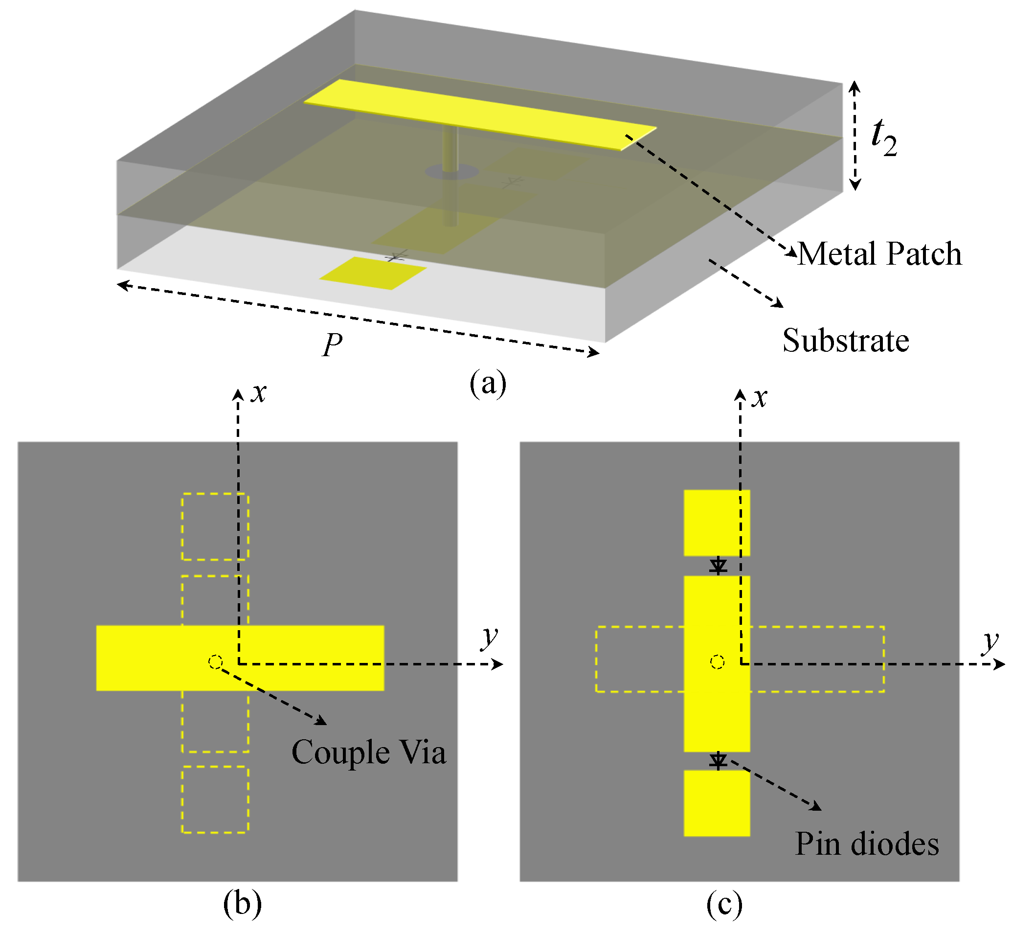
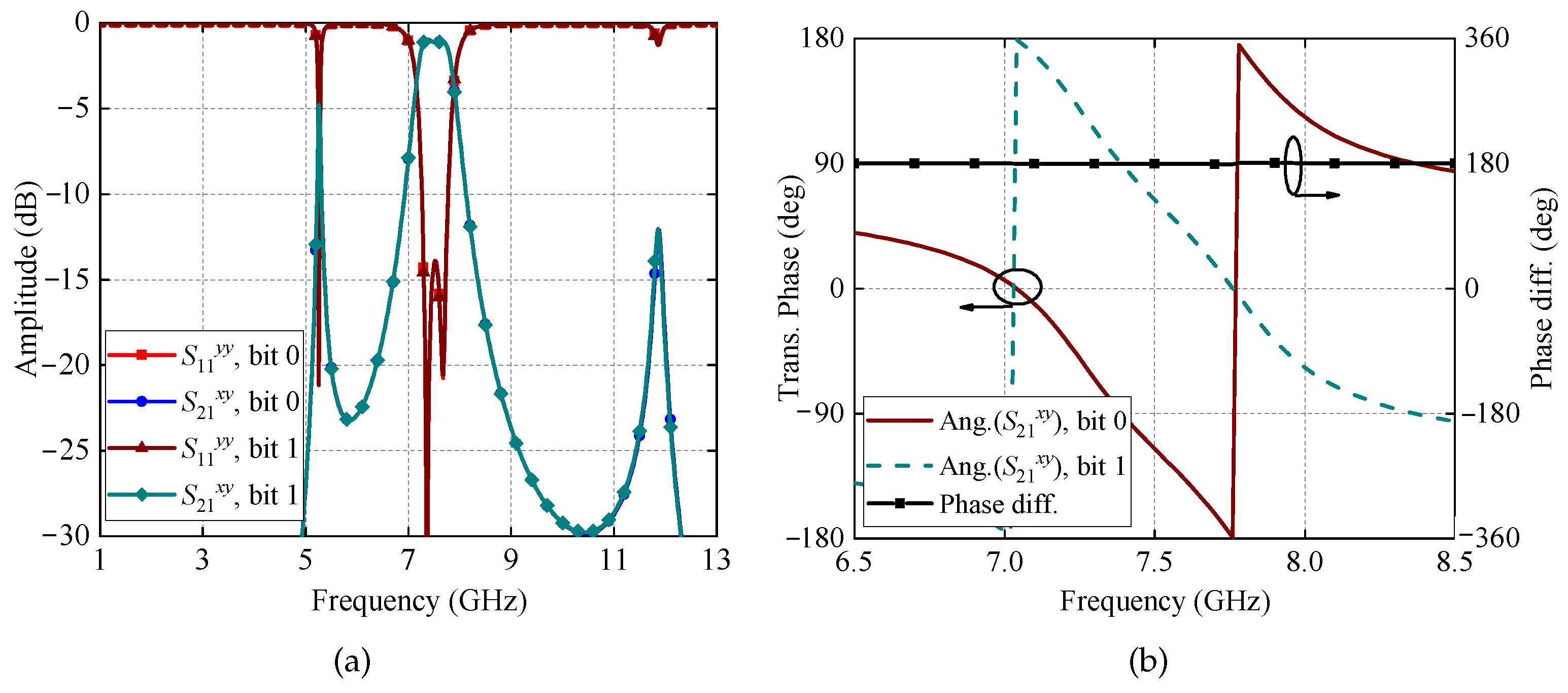
3.2. 1-Bit RTA Element
After the design and analysis of the AFST, the next step is to design the 1-bit RTA element. As mentioned in Section 2, the RTA structure must meet two key requirements. The first is to provide low-insertion-loss transmission and 1-bit phase regulation at GHz to enable in-band high-gain and beam scanning performance. The second is to maintain perfect reflection characteristics near GHz and GHz to ensure the out-of-band high absorptivity performance of the AFST.
The proposed 1-bit RTA element is shown in Figure 7, which employs a receiver–transmitter structure with an active receiving dipole and a passive asymmetric transmitting dipole. Both dipoles, separated by a common ground and connected by a metallized via-hole, are linearly polarized and aligned in the orthogonal direction. Two pin diodes are integrated on the active dipole and biased in opposite states to reverse the current on the active dipole, which essentially results in a 180° phase difference, thus enabling a wideband 1-bit phase. The ON and OFF states of the pin diode are modeled as and series circuits, respectively [26]. Specifically, in the ON state, the resistance and inductance are and nH, respectively. In the OFF state, the resistance, inductance, and capacitance are , nH, and pF, respectively. The element has a period P of 20 mm, a thickness of 4 mm, and a substrate with a relative dielectric constant of 3.
Figure 7.
Element of the proposed 1-bit RTA: (a) perspective view, (b) top view, and (c) bottom view.
Figure 8 illustrates the simulated S parameters of the designed RTA, including its amplitude and phase. The results indicate that the structure has achieved a good polarization converter transmission performance in 7.3∼7.75 GHz, with two resonant frequencies in the band. These resonant frequencies are generated by the half-wavelength resonance of the top dipole, which are then differentiated into two frequencies through the coupling of the metallic via-hole. The insertion loss of the passband is approximately 1.2 dB, which is mainly attributed to the resistance loss of the pin diode. Furthermore, Figure 8b depicts the transmission phase under different states, demonstrating that a 180° phase difference can be constructed within the transmission band through the pin diode, thus achieving a 1-bit electronic RTA.
Figure 8.
Simulated S parameters of the 1-bit RTA element under different states: (a) amplitudes and (b) phase.
However, it should be noted that the structure has an unexpected resonance point near 5.3 GHz, which may deteriorate the absorption performance of the AFST at this frequency. Therefore, it is necessary to eliminate this resonance frequency. Through observing the current distribution at the resonant frequency of 5.3 GHz, as shown in Figure 9a, an unwanted resonant path is generated through the bottom dipole, via-hole and the top dipole, as indicated by the black dotted line. To break this resonance, a shorted metallic via-hole is added to the top dipole to forcibly change the resonant path, as shown in Figure 9b. It can be seen that the resonant path is broken because it is connected to GND through the shorted via-hole, thus the polarization converter transmission performance will be eliminated. Figure 9c shows the simulated S parameter after adding the shorted via-hole. It can be observed that although the resonant frequency at 5.3 GHz moves to 6.25 GHz, the co-polarized reflection coefficient at this frequency is greater than −1 dB, which has little influence on the out-of-band absorption performance. Notably, the shorted via-hole can also be reused as a ground through-hole for the biasing voltage, providing a 0 V voltage to the pin diode.

Figure 9.
Simulated current distribution of the RTA at 5.3 GHz (a) without and (b) with shorted via-hole, and (c) the simulated S parameters with shorted via-hole.
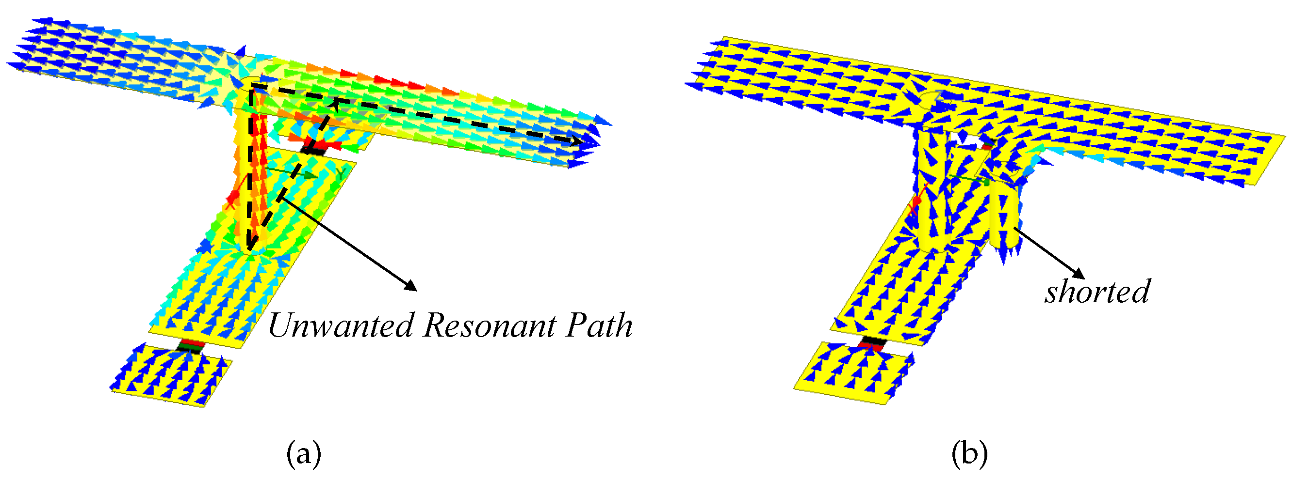
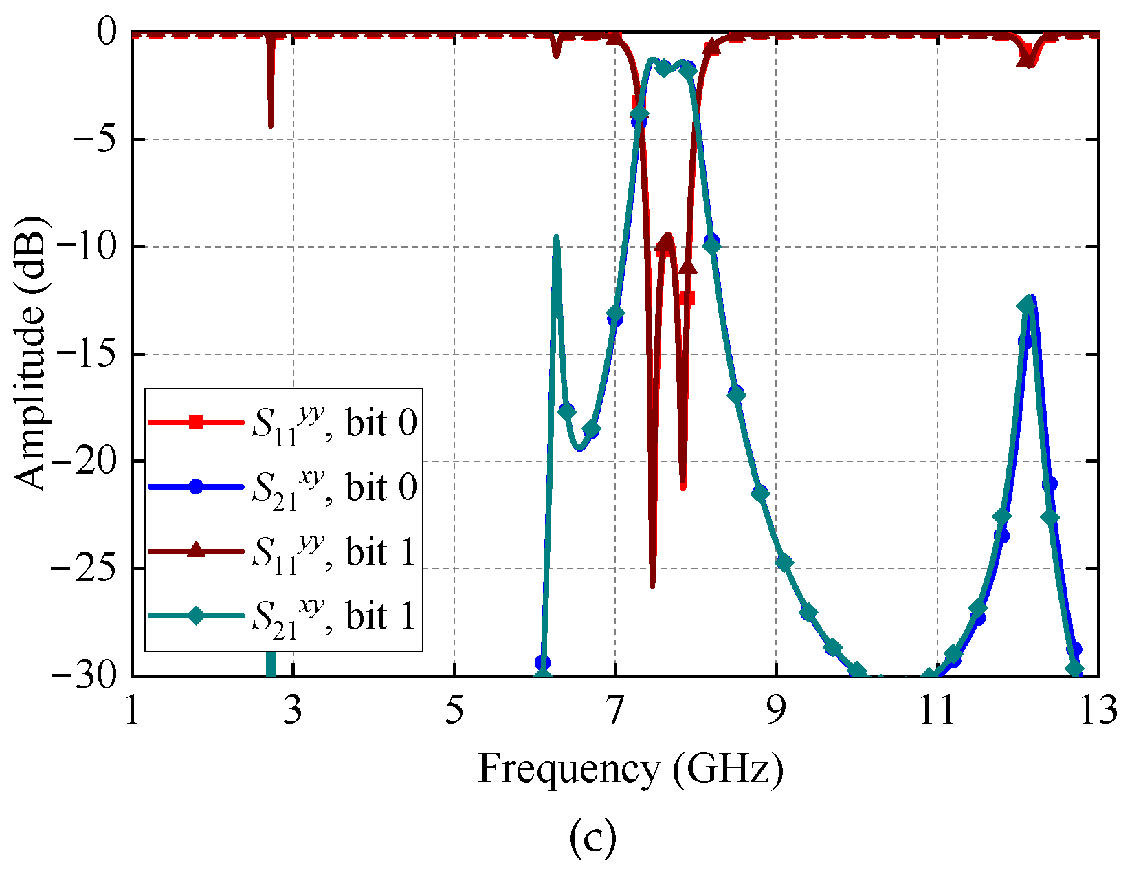
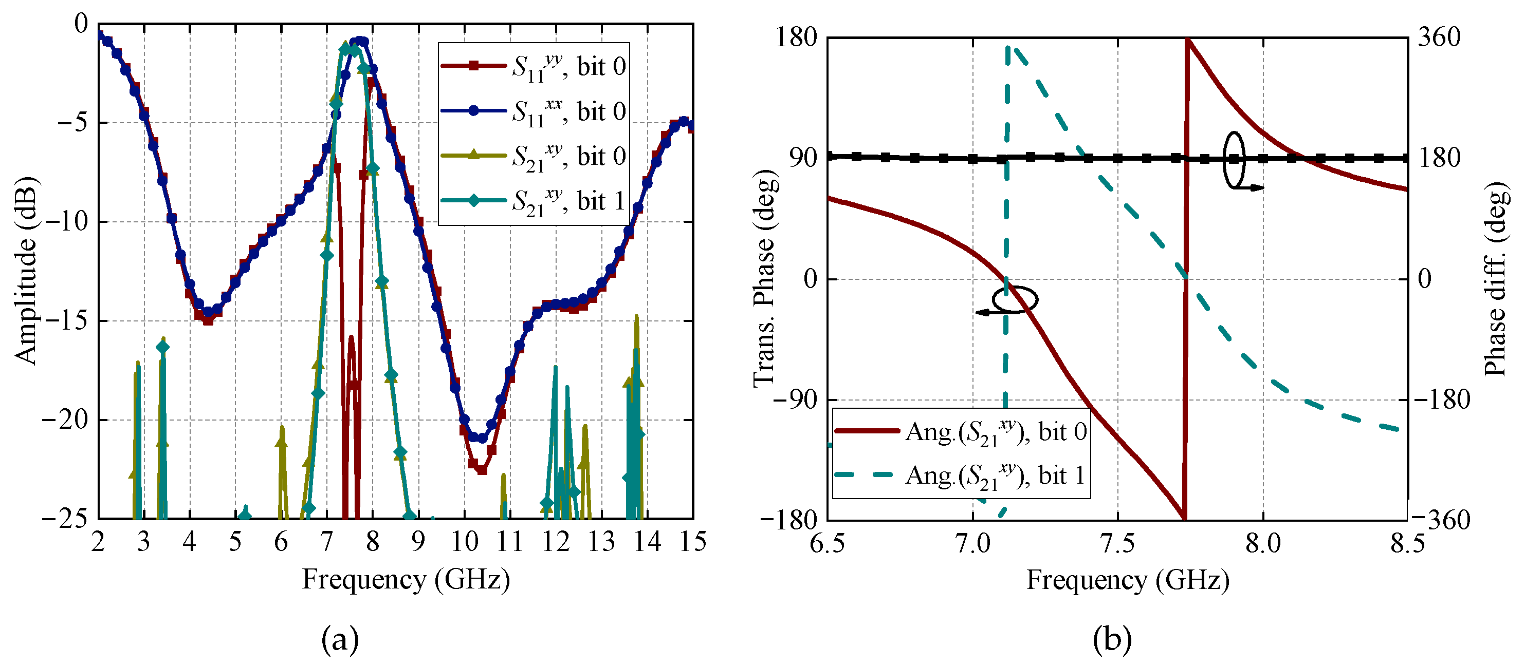
3.3. Low RCS 1-Bit RTA Element
The element of the low RCS 1-bit RTA is constructed by integrating the AFST and 1-bit RTA according to the design concepts in Section 2, as shown in Figure 10a. The AFST and RTA layers are separated by an air layer with a thickness h of 6 mm, which is the result of an optimization that balances the low- and high-frequency absorption performance. Meanwhile, the biasing lines of the RTA are given in Figure 10b. For each receiver–transmitter structure, the middle portion of the active receiving dipole is grounded through the passive transmitter dipole, while a +2.5/−2.5 V DC biasing voltage is applied to both ends of the active receiving dipole to control the pin diode states. The open-ended radial stubs on the receiving layer are designed to choke the RF leakage. The biasing point is positioned close to the zero point of the electric field to minimize the influence of the bias lines on the RF performance. The remaining parameters of the structure are listed as follows: mm, mm, mm, and mm. The diameter of the coupling metallic via-hole is mm. Its position is 1.2 mm away from the center of the top dipole and located in the center of the bottom dipole.
Figure 10.
Element of the proposed low-RCS 1-bit RTA: (a) perspective view, (b) bottom view.
The element of the proposed low-RCS 1-bit RTA was simulated using HFSS simulation software, and the amplitudes and phases are illustrated in Figure 11. From Figure 11a, it is found that the out-of-band reflection coefficient is less than −10 dB, which indicates that the incident wave is effectively absorbed, whether it is x- or y-polarization. Therefore, the designed structure realizes wideband dual-polarization absorption. Additionally, it exhibits a good trans-polarized transmission performance and 1-bit phase reconfiguration around 7.5 GHz for y-polarization incidence. Consequently, the design is capable of suppressing out-of-band scattering and achieving in-band high-gain radiation and beam scanning performance.
Figure 11.
Simulated S parameters of the low-RCS 1-bit RTA element under different bit states: (a) amplitudes, (b) phase.
4. Experimental Verification
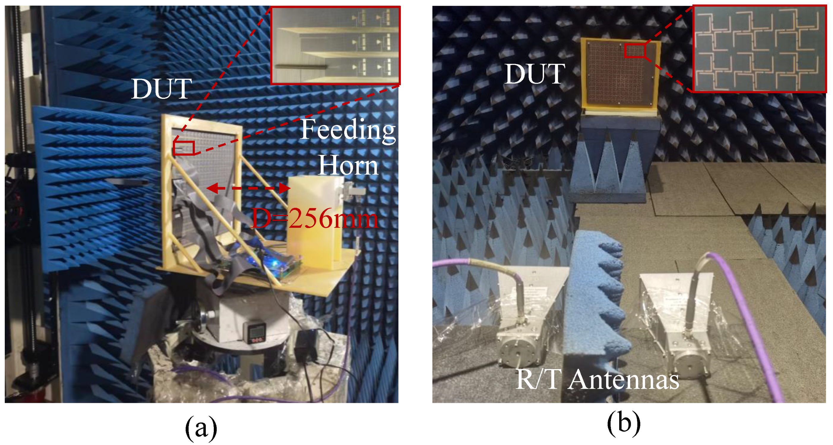
4.1. Antenna Prototype and Measurement Setup
The operating frequency and the size of the array can be expanded according to the actual application scenario. Certainly, larger arrays and a higher operating frequency are bound to bring about rapid increases in manufacturing difficulty and cost, and also the number of control hardware and logical complexity. Therefore, the array size and operating frequency should be assessed and balanced according to the actual situation. As an example, a 16 × 16 low-RCS 1-bit RTA prototype was designed, fabricated, and measured based on the element structure, as illustrated in Figure 12. The prototype has an effective aperture of 320 mm × 320 mm and integrates 512 pin diodes (SMP1340-040LF, Skyworks, Shanghai, China). Additionally, there are 4 × 64 pin connectors located on the sides of the array, which are connected to the FPGA control board to enable the electronic control of each element’s state.
Figure 12.
Measured setups for (a) radiation and (b) RCS reduction performance.
The AFST layer is placed above the RTA layer using 16 plastic struts. It should be pointed out that compared with the traditional transmitarray antenna, the designed low-RCS 1-bit RTA significantly reduces the out-of-band RCS and has the in-band beam scanning capability, which greatly broadens its application range, although an additional AFST layer and PIN diode are added, resulting in complex manufacturing and increased cost. Moreover, the AFST layer uses a multimode resonant structure, which simplifies the structure complexity and reduces the antenna profile. Moreover, a linearly polarized horn antenna is used as the feed to excite the RTA, with a focal–diameter ratio of 0.8. In the case of beam scanning, the actual compensation phase for each element in a different beam scanning angle can be calculated using the following formulas [27]:
where and are the phase differences of the element position and beam scanning, is the reference phase, and is the wavelength corresponding to 7.5 GHz. Then, the bit state of each element can be obtained using the following formula [28]:
The measurement process consists of two parts: RCS reduction evaluation and radiation performance measurement. Therefore, two different measurement systems are set up to complete the measurement process, as illustrated in Figure 12. The setup shown in Figure 12a has the prototype in a near-field anechoic chamber and acts as a transmitting antenna to measure its beam scanning performance. On the other hand, the fabricated prototype was placed in an anechoic chamber that was irradiated with a pair of linearly polarized horn antennas. Then, the reflection coefficient differences caused by adding an AFST layer to the RTA layer was calculated, which can be used to characterize the RCS reduction, as shown in Figure 12b. During the measurements, the environment noise of the anechoic chamber is about −80 dBm, and the signal-to-noise ratio can be guaranteed to be about 30 dB.
Furthermore, the following two aspects were applied to ensure the measurement accuracy. First, the feed antenna and the receiving waveguide should be aligned with the center of the array. Therefore, a bracket was machined using 3D printed technology to ensure the accuracy of antenna erection, as shown in Figure 12a. Second, the influence of the multipath effect should be reduced as much as possible when measuring the RCS reduction performance of the antenna. Therefore, a window function was added to the echo signal to filter out the multipath signal.
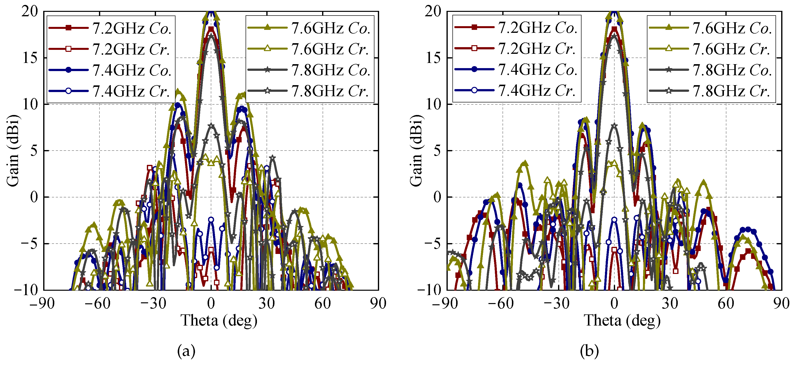
4.2. Radiation Performance
The simulated and measured gain of the designed low-RCS 1-bit RTA prototype at different frequencies is illustrated in Figure 13. It is seen that loading the AFST on top of the 1-bit RTA will result in a gain loss of about 1 dB. The measured realized gain at 7.5 GHz is approximately 20.1 dBi, with a corresponding aperture efficiency of 12.7%, and the 3 dB gain bandwidth is about 8.7%. Moreover, the radiation efficiency of the design RTA is around 65∼70%. Compared to the simulated results, the measured gain is reduced by approximately 0.6 dB, and the gain bandwidth is also slightly reduced. In taking into account machining and measured errors, the slight warping of the AFST layer, and the parasitic effect of the pin diode, the results are considered acceptable.
Figure 13.
Simulated and measured gain of the designed low-RCS 1-bit RTA and its corresponding aperture efficiency.
The simulated broadside radiation patterns at different frequencies are presented in Figure 14. It is seen that the designed antenna has a relatively stable co-polarized pattern in the operating band, while the cross-polarized level gradually deteriorates as the frequency approaches the edge of the band. In addition, the sidelobe levels of the pattern in the H-plane are relatively stable compared with those of the E-plane.
Figure 14.
Simulated broadside radiation patterns at different frequencies. (a) E-plane and (b) H-plane.
The simulated and measured broadside radiation patterns at 7.5 GHz are shown in Figure 15. It is found that the simulated and measured results are in good agreement. The measured half-power beamwidths (HPBWs) are 10.4° and 10.8° in the E- and H-planes, respectively. Additionally, the measured cross-polarized level is less than −20 dB in both principal planes. The simulated and measured beam scanning performances at 7.5 GHz in both principal planes are shown in Figure 16. It is evident that the beam accurately reaches the expected direction within the range of 60°, and the scanning gain loss is about 5 dB in both principal planes, which is mainly affected by the phase compensation errors. This can be addressed using either two-bit phase compensation or smaller array elements.
Figure 15.
Simulated and measured broadside radiation patterns at 7.5 GHz. (a) E-plane. (b) H-plane.
Figure 16.
Simulated and measured beam scanning performance at 7.5 GHz in (a) E-plane and (b) H-plane.
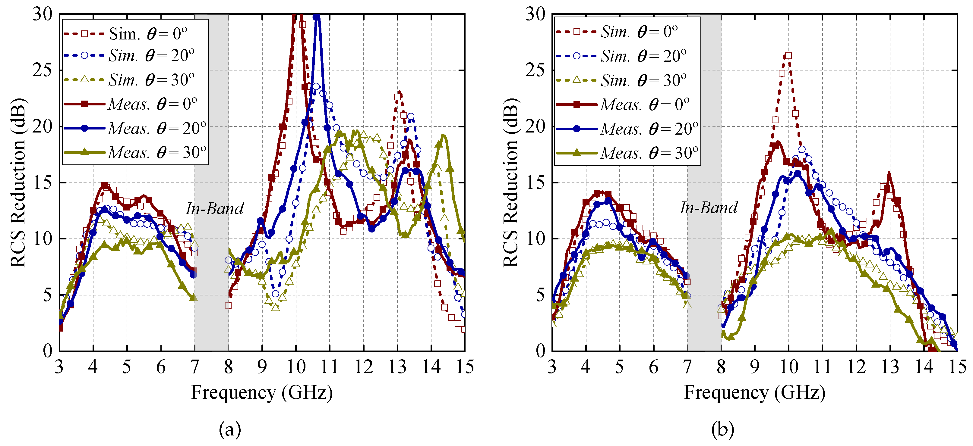
4.3. RCS Reduction Performance
The RCS reduction performance of the prototype can be observed from the simulated and measured results. The simulated results are obtained using the CST 2021 commercial simulation software with plane wave excitation and open boundary conditions. It is seen that the integration of AFST on top of the RTA effectively reduces the out-of-band RCS under both the TE and TM polarized incident waves, as shown in Figure 17. Specifically, the 10 dB RCS reduction bandwidth for low and high frequencies is 52.5% and 43.8%, respectively. The RCS reduction performance under oblique incidences is given in Figure 18. It is found that the RCS reduction performance of low frequency is relatively stable at oblique incidence, while the RCS reduction performance of high frequency has band shift. In general, in the case of a 30° oblique incidence, the designed low-RCS 1-bit RTA can maintain a relatively stable RCS reduction performance.
Figure 17.
Simulated monostatic RCS of the 1-bit RTA with and without AFST for both TE and TM polarization.
Figure 18.
Simulated and measured RCS reduction with various incident angles for (a) TE and (b) TM polarization.
4.4. Comparison and Discussion
In order to demonstrate the advantages of the designed low-RCS 1-bit RTA, it was compared with other published works in terms of RCS reduction and radiation performance. Considering that there is little research focus on reducing the RCS of RTAs, we compared the radiation performance with conventional 1-bit RTAs with an approximate operating frequency and gain, and compared the RCS reduction performance with a low-RCS transmitarray. It can be seen from Table 1 that, compared with existing low-RCS transmitarray antennas, our work obtains a lower profile due to the effective use of multiple resonances, and the bandwidths of the low- and high-RCS reduction band are relatively wide. Furthermore, the beam scanning capability is introduced, reflecting the advanced performance of our work.
Table 1.
RCS reduction comparison for low-RCS transmitarray.
On the other hand, the disadvantages of the proposed design is that additional resistors need to be introduced, resulting in increased structural complexity and cost compared to traditional RTAs that do not provide RCS reduction. In addition, placing an AFST layer above the RTA layer results in a slight deterioration in radiation gain, as shown in Table 2. However, out-of-band RCS is effectively reduced in return. While compared with phased array antennas, the designed 1-bit RTA can greatly reduce the cost because it does not require the T/R component. Furthermore, reducing the RCS by diffusing the incident wave over the entire visible space can effectively avoid the use of resistors. At the same time, the effect on radiation gain can be eliminated by integrating stealth and radiation functions into the same simple structure through multimode resonant structure. In summary, the designed low-RCS 1-bit RTA is a promising candidate for use in radar systems and other related applications, especially for application scenarios requiring a large radiation aperture surface, fast beam switching, and stealth.
Table 2.
Radiation performance comparison for 1-bit RTA.
5. Conclusions
This paper presents a 1-bit RTA with out-of-band RCS reduction, consisting of AFST and RTA layers. The AFST layer uses the first three resonant modes of a bent metallic strip with a centrally loaded resistor to achieve out-of-band scattering suppression and in-band transmission. Meanwhile, the RTA layer adopts a receiver–transmitter structure with an active receiving dipole and a passive orthogonal transmitting dipole to achieve 1-bit transmission phase reconfiguration. Subsequently, a 16 × 16-element prototype was designed and measured, revealing in-band high-gain radiation and beam scanning capabilities, along with out-of-band wideband RCS reduction. For radiation, the measured gain was 20.1 dBi at 7.5 GHz, corresponding to an aperture efficiency of 12.7%. The gain loss of beam scans to ±60° was about 5 dB in both principal planes. For scattering, the bandwidth of 10 dB RCS reduction was about 52.5% and 43.8%, respectively.
Author Contributions
Conceptualization, F.Y. and S.X.; validation, M.L., writing and methodology, B.Z.; review and editing, W.H. All authors have read and agreed to the published version of the manuscript.
Funding
This research was funded by the National Natural Science Foundation of China under Grant 62401314, and in part by the YoungElite Scientists Sponsorship Program by CAST under Grant 2023QNRC001.
Institutional Review Board Statement
Not applicable.
Informed Consent Statement
Not applicable.
Data Availability Statement
The original contributions presented in this study are included in the article. Further inquiries can be directed to the corresponding author.
Conflicts of Interest
The authors declare no conflicts of interest.
Abbreviations
The following abbreviations are used in this manuscript:
| RTA | reconfigurable transmitarray antenna |
| RRA | reconfigurable refelctarray antenna |
| RCS | radar cross-section |
| AFST | absorptive frequency selective transmission |
| FSS | frequency selective surface |
| HPBW | half-power beamwidth |
References
- Yusuf, Y.; Gong, X. A low-cost patch antenna phased array with analog beam steering using mutual coupling and reactive loading. IEEE Antennas Wirel. Propag. Lett. 2008, 7, 81–84. [Google Scholar] [CrossRef]
- Zhang, H.; Chen, X.; Wang, Z.; Ge, Y.; Pu, J. A 1-Bit electronically reconfigurable reflectarray antenna in X band. IEEE Access 2019, 7, 66567–66575. [Google Scholar] [CrossRef]
- Pham, K.T.; Clemente, A.; Blanco, D.; Sauleau, R. Dual-circularly polarized high-gain transmitarray antennas at Ka-band. IEEE Trans. Antennas Propag. 2020, 68, 7223–7227. [Google Scholar] [CrossRef]
- Jia, Y.; Liu, Y.; Gong, S.; Zhang, W.; Liao, G. A low-RCS and high-gain circularly polarized antenna eith a low profile. IEEE Antennas Wirel. Propag. Lett. 2017, 16, 2477–2480. [Google Scholar] [CrossRef]
- Wang, Y.; Ge, Y.; Chen, Z.; Zhou, Z. Design of wideband reflectarray and transmitarray antennas with low sidelobe and cross-polarization levels using a multifunctional ultrathin metasurface. IEEE Open J. Antennas Propag. 2024, 5, 601–611. [Google Scholar] [CrossRef]
- Tian, C.; Jiao, Y.-C.; Zhao, G.; Wang, H. A wideband transmitarray using triple-layer elements combined with cross slots and double square rings. IEEE Antennas Wirel. Propag. Lett. 2017, 16, 1561–1564. [Google Scholar] [CrossRef]
- Palma, L.D.; Clemente, A.; Dussopt, L.; Sauleau, R.; Potier, P.; Pouliguen, P. Circularly polarized transmitarray with sequential rotation in Ka-band. IEEE Trans. Antennas Propag. 2015, 63, 5118–5124. [Google Scholar] [CrossRef]
- Li, T.-J.; Wang, G.-M.; Cai, T.; Li, H.-P.; Liang, J.-G.; Lou, J. Broadband folded transmitarray antenna with ultralow-profile based on metasurfaces. IEEE Trans. Antennas Propag. 2021, 69, 7017–7022. [Google Scholar] [CrossRef]
- Tong, Y.; Cao, W.; Wang, C.; Zhu, Y. A Wideband Low-RCS transmitarray with high aperture efficiency based on grooved metasurface. IEEE Antennas Wirel. Propag. Lett. 2024, 23, 2170–2174. [Google Scholar] [CrossRef]
- Feng, P.-Y.; Qu, S.-W.; Yang, S. Dual-polarized filtering transmitarray antennas with low-scattering characteristic. IEEE Trans. Antennas Propag. 2021, 69, 7965–7970. [Google Scholar] [CrossRef]
- Feng, P.-Y.; Qu, S.-W.; Chan, K.F.; Yang, S.; Chan, C.H. Integrative transmitarray with gain-filtering and low-scattering characteristics. IEEE Trans. Antennas Propag. 2022, 70, 1931–1939. [Google Scholar] [CrossRef]
- Wang, X.; Qin, P.-Y.; Jin, R. Low RCS transmitarray employing phase controllable absorptive frequency-selective transmission elements. IEEE Trans. Antennas Propag. 2021, 69, 2398–2403. [Google Scholar] [CrossRef]
- Zhang, Z.; Cao, X.; Yang, H.; Li, T.; Li, S.; Ji, K. Phase controllable FSR design and its application into a high-gain transmitarray antenna with a low radar cross-section. J. Phys. D Appl. Phys. 2022, 55, 015103. [Google Scholar] [CrossRef]
- Lu, J.; Cao, X.; Cong, L.; Ji, K.; Cao, K. Design of low-RCS broadband high-gain antennas based on transmission array metasurface. Micromachines 2022, 13, 1614. [Google Scholar] [CrossRef]
- Li, M.; Shen, Z. Low-RCS transmitarray based on 2.5-D cross-polarization converter. IEEE Trans. Antennas Propag. 2023, 71, 5828–5837. [Google Scholar] [CrossRef]
- Wang, M.; Xu, S.; Yang, F.; Li, M. Design and measurement of a 1-bit reconfigurable transmitarray with subwavelength H-shaped coupling slot elements. IEEE Trans. Antennas Propag. 2019, 67, 3500–3504. [Google Scholar] [CrossRef]
- Clemente, A.; Dussopt, L.; Sauleau, R.; Potier, P.; Pouliguen, P. Wideband 400-element electronically reconfigurable transmitarray in X band. IEEE Trans. Antennas Propag. 2013, 61, 5017–5027. [Google Scholar] [CrossRef]
- Wang, Z.; Ge, Y.; Pu, J.; Chen, X.; Li, G.; Wang, Y.; Liu, K.; Zhang, H.; Chen, Z. 1-bit electronically reconfigurable folded reflectarray antenna based on p-i-n diodes for wide-angle beam-scanning applications. IEEE Trans. Antennas Propag. 2020, 68, 6806–6810. [Google Scholar] [CrossRef]
- Wang, X.; Qin, P.-Y.; Le, A.T.; Zhang, H.; Jin, R.; Guo, Y.J. Beam scanning transmitarray employing reconfigurable dual-layer huygens element. IEEE Trans. Antennas Propag. 2022, 70, 7491–7500. [Google Scholar] [CrossRef]
- Plaza, E.G.; León, G.; Loredo, S.; Arboleya, A.; Las-Heras, F.; Álvarez, C.M.S.; Rodriguez-Pino, M. An ultrathin 2-bit near-field transmitarray lens. IEEE Antennas Wirel. Propag. Lett. 2017, 16, 1784–1787. [Google Scholar]
- Diaby, F.; Clemente, A.; Sauleau, R.; Pham, K.T.; Dussopt, L. 2 bit reconfigurable unit-cell and electronically steerable transmitarray at Ka-band. IEEE Trans. Antennas Propag. 2020, 68, 5003–5008. [Google Scholar] [CrossRef]
- Fan, G.; Cheng, Q. 1-bit electronically reconfigurable transmitarray antenna with RCS reduced flexibly. In Proceedings of the 2021 IEEE International Workshop on Electromagnetics: Applications and Student Innovation Competition (iWEM), Guangzhou, China, 28–30 November 2021; pp. 1–3. [Google Scholar]
- Zhang, B.; Yang, F.; Xu, S.; Li, M. Design of a low RCS 1 bit electronically reconfigurable transmitarray antenna. In Proceedings of the 2023 International Conference on Microwave and Millimeter Wave Technology (ICMMT), Qingdao, China, 14–17 May 2023; pp. 1–3. [Google Scholar]
- Kang, N.; Jin, C.; Zhang, B.; Lv, Q.; Wang, J.; Tian, B. Design of wideband microwave absorber with ultra-wide-angle response. In Proceedings of the 2021 Photonics Electromagnetics Research Symposium (PIERS), Hangzhou, China, 21–25 November 2021; pp. 2593–2596. [Google Scholar]
- Lu, W.; Zhu, L. A novel wideband slotline antenna with dual resonances: Principle and design. IEEE Antennas Wirel. Propag. Lett. 2015, 14, 795–798. [Google Scholar] [CrossRef]
- Wang, M.; Xu, S.; Yang, F.; Li, M. A 1-bit bidirectional reconfigurable transmit-reflectarray using a single-layer slot element with PIN diodes. IEEE Trans. Antennas Propag. 2021, 6, 6205–6210. [Google Scholar]
- Zhou, S.-G.; Zhao, G.; Xu, H.; Luo, C.-W.; Sun, J.-Q.; Chen, G.-T.; Jiao, Y.-C. A wideband 1-bit reconfigurable reflectarray antenna at Ku-band. IEEE Antennas Wireless. Propag. Lett. 2022, 21, 566–570. [Google Scholar] [CrossRef]
- Luo, C.-W.; Zhao, G.; Jiao, Y.-C.; Chen, G.-T.; Yan, Y.-D. Wideband 1 bit reconfigurable transmitarray antenna based on polarization rotation element. IEEE Antennas Wireless. Propag. Lett. 2021, 20, 798–802. [Google Scholar] [CrossRef]
Disclaimer/Publisher’s Note: The statements, opinions and data contained in all publications are solely those of the individual author(s) and contributor(s) and not of MDPI and/or the editor(s). MDPI and/or the editor(s) disclaim responsibility for any injury to people or property resulting from any ideas, methods, instructions or products referred to in the content. |
© 2024 by the authors. Licensee MDPI, Basel, Switzerland. This article is an open access article distributed under the terms and conditions of the Creative Commons Attribution (CC BY) license (https://creativecommons.org/licenses/by/4.0/).