Featured Application
Protection and encryption of digital files using hardware fingerprinting. Using an XOR Gate, two Static Random-Access Memory (SRAM) PUFs’ challenge–response pairs (CRPs) can be combined into a single larger SRAM PUF.
Abstract
This study focuses on designing enhanced Physically Unclonable Functions (PUFs) based on SRAM devices and improving the security of cryptographic systems. Most SRAM PUFs are limited in their number of CRPs, which makes them vulnerable to enrollment attacks. In this research, we present an SRAM-based PUF design that greatly increases the number of CRPs and the entropy of the generated bits by performing exclusive-or (XOR) on the responses of two SRAM devices. This was implemented using a readily available development board, SRAM devices, and a user-friendly custom circuit board for cryptographic key generation. The cryptographic protocol was implemented using both C++ and python3. The proposed SRAM PUF design was experimentally demonstrated and showed substantial improvements in the security of various cryptographic applications as a hardware authentication device. It also addresses the specific vulnerabilities of legacy designs.
1. Introduction
In modern cryptography, a combination of asymmetric and symmetric encryption protocols, such as Advanced Encryption Standards (AES) and Rivest–Shamir–Adleman (RSA), are commonly used to secure digital communications or hardware authentication devices. Although effective for many applications, these methods have inherent vulnerabilities, such as the need to store private keys in non-volatile memory, which can be non-invasively stolen [1,2]. The security of such systems can be enhanced by using Physically Unclonable Functions (PUFs), which can generate keys for both symmetrical and asymmetrical encryption, thereby eliminating the need to store private keys. The approach offers multiple options, such as key generation on demand, one-time keys, multi-factor authentications, or random number generation.
PUFs leverage the inherent randomness of the manufacturing process to create unique digital ‘fingerprints’ that behave as a one-way function, mapping challenges to responses. These ‘fingerprints’ are stochastic and can be used to generate cryptographic keys or random numbers. PUFs are relatively simple to use and consume little power, making them highly desirable in cryptographic applications.
Among the various PUF technologies, a Static Random-Access Memory (SRAM) PUF is the most prevalent, as electronic devices worldwide already ship with SRAM chips. SRAM is mass-produced, which indicates an existing supply chain and affordable manufacturing costs. Several benefits exist when using SRAM to create a PUF, including simplicity, energy efficiency, and ubiquity. The downside is that SRAM PUFs suffer from a limited number of challenge–response pairs with large bit-error rates [3], vulnerability to cloning [4], and aging problems [5,6].
This study presents a new design for an SRAM PUF that addresses some of the challenges currently faced by SRAM PUF designs. The proposed design incorporates two SRAM devices to enhance the entropy and number of CRPs while retaining the ability to generate reliable bits. To evaluate the effectiveness of this design, we collect several critical PUF metrics, such as inter-chip distance, bit-error rate (BER), latency, and entropy. The data gathered from these metrics provide insights into the reliability and security of the proposed design.
The first section of this paper goes over the background of SRAM and PUFs. It discusses the techniques used to create an SRAM PUF, along with our contributions to the field using the XOR SRAM PUF. The following section will discuss the devices used, along with the actual design of the XOR SRAM PUF and how key generation was performed. Afterward, the characterization section will discuss the benchmarks used to compare the XOR SRAM PUF and how it retains the desirable properties of the SRAM PUF while improving several other aspects. Finally, potential future work will be considered to improve the design further to be more applicable to the current SRAM PUF usage.
2. Background
2.1. SRAM Technology
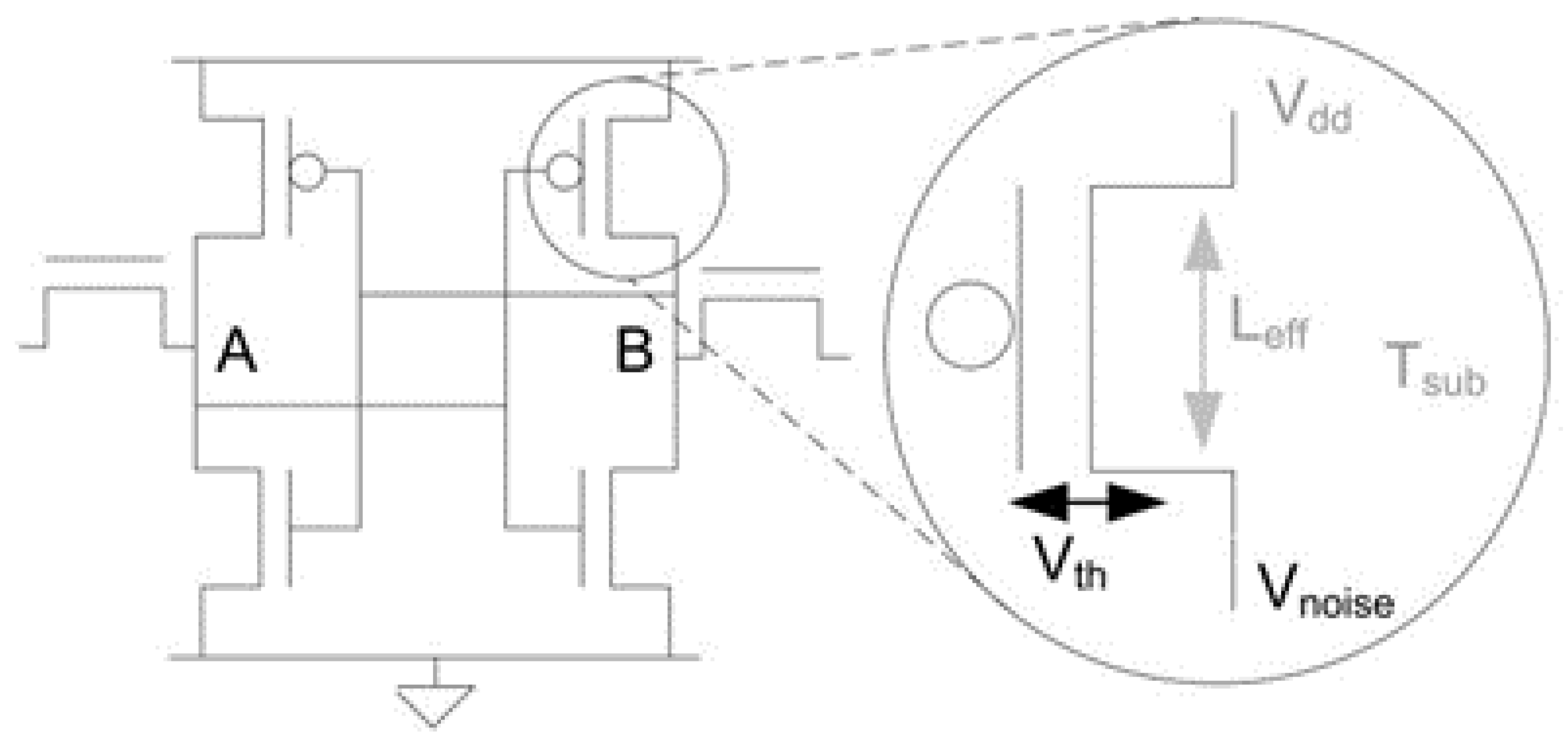
SRAM is a type of volatile random-access memory that employs latching circuitry to retain information as long as it is powered. A typical CMOS SRAM cell comprises four to six transistors arranged in a specific configuration that forms a flip-flop circuit. The transistors are typically divided into two cross-coupled inverters. The cross-coupled inverters store and amplify the bit of data stored in the SRAM cell, as shown in Figure 1 [7]. When an SRAM cell is powered on, it will wake in an initial state, ‘0’ or ‘1’. The threshold voltage of the cross-coupled transistors determines the initial state of an SRAM cell. Due to small variations during the manufacturing process and asymmetries in the coupled transistors, the exact threshold voltage per device follows a random distribution. As a result, ideal SRAM cells should have an even random split of ‘0’s and ‘1’s when initially powered on, as both inverters have exactly the same threshold voltage.

Figure 1.
Six- transistor SRAM cell [7].
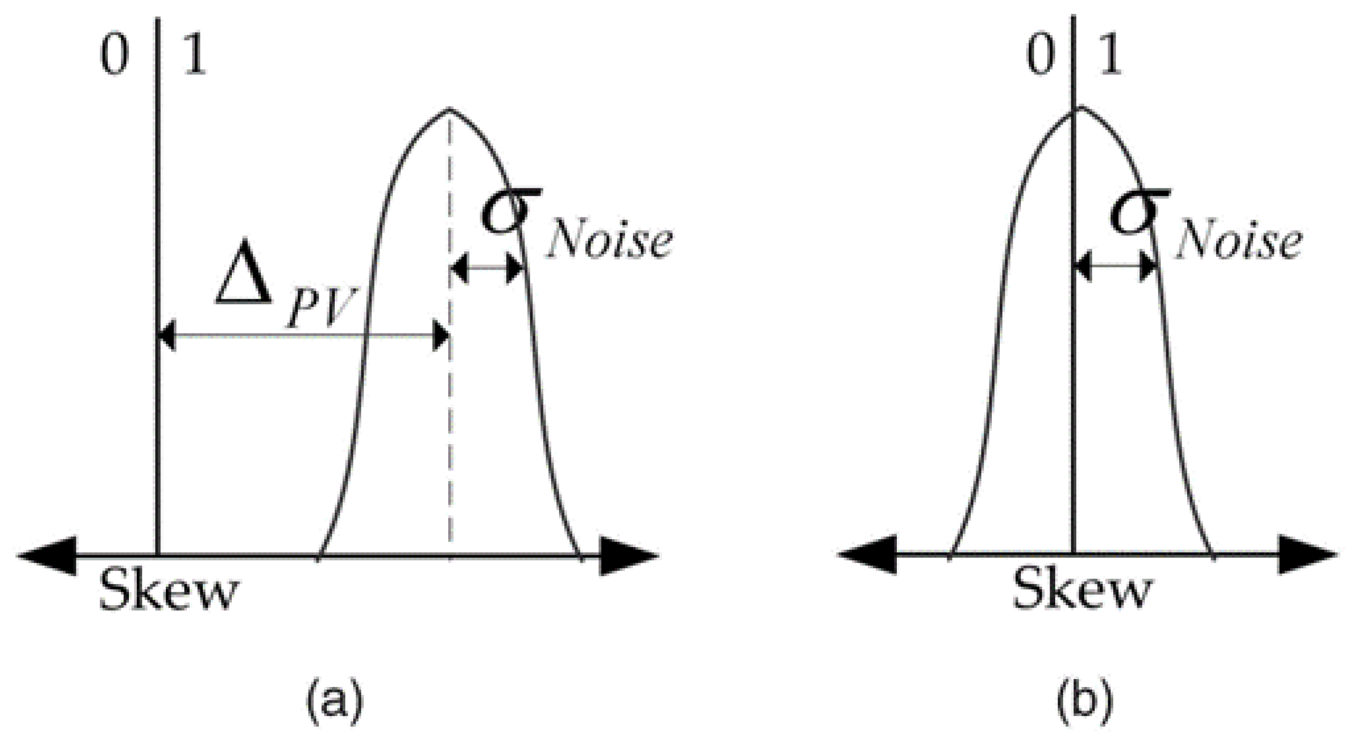
However, most SRAM cells have substantial threshold differences, leading to a heavily skewed initial state of a strong ‘0’ or ‘1’. Conversely, a low threshold difference leaves a state susceptible to noise, where its initial state can be either a ‘0’ or ‘1’, as illustrated in Figure 2. When the objective is the design of PUFs, SRAM cells that exhibit small differences in threshold voltage are often referred to as flaky or fuzzy. These cells switch easily between the two states on start-up, leading to unpredictable behavior. In addition to the threshold voltage differences, there can be many other small parameters resulting from the fabrication process that can cause the cells to assume a strong ‘0’ or ‘1’ state or exhibit flaky behavior, making each device unique and unclonable.
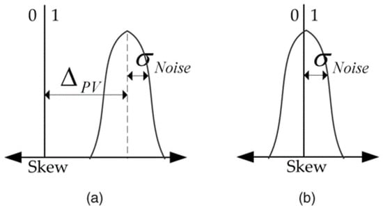
Figure 2.
Strong vs. flaky cell: (a) The skew of a strong 1. (b) The skew of a flaky cell. In these figures, skew represents the delta (Vt) of the devices [7].
2.2. Physically Unclonable Functions
A PUF operates as a ’black box’ by mapping inputs (challenges) to outputs (responses) using its inherent randomness derived from the manufacturing process. By mapping every challenge and response to expected CRPs, an enrollment of the PUF can be created for future challenges against the PUF.
Current forms of information security require hardware authentication devices for high-security situations. Current commercial forms of the technology require storing an internal secret that is used to generate a key for the user [8]. Using side-channel attacks, these internal secrets can be leaked without compromising the device. In contrast to this, the PUF generates private keys from measurements of the SRAM rather than storage on the device. This measurement results in PUFs being more resilient to side-channel attacks than devices that operate on a single hidden key. Due to their resilience, PUFs can provide a portable second factor of authentication with a massive possible CRP space compared to many public alternatives.
While the term ’PUF’ was not formally introduced until 2002 by Gassend et al. in [9], using a device’s physical characteristics for security purposes traces back to Simmons’s work in 1984 [10]. Since their introduction, various types of PUFs have been proposed. Gate-delay PUFs were among the first types of PUFs proposed [11,12,13]. These PUFs exploited the manufacturing variability of digital gates to generate their responses. Afterward, memory PUFs were proposed; these PUFs exploited the manufacturing variability of various memory technologies to generate their responses. Among them were SRAM [3,7,14], resistive random-access memory (ReRAM) [15,16,17], and magnetoresistive random-access memory (MRAM) [18,19].
The quality of PUFs is based on certain metrics, such as inter-chip distance (uniqueness), BER (reliability), and entropy (randomness):
- The inter-chip Hamming Distance () is a metric used to measure the uniqueness of PUFs. is the Hamming Distance between the responses generated by two different PUF configurations when presented with the same challenge, divided by the total number of responses. In an ideal scenario, this value should be 0.50, indicating that the two PUF configurations produce completely distinct and different responses.
- The reliability of a PUF can be quantified by measuring its bit-error rate (s) and intra-chip distance. The BER is calculated as the rate of discrepancies between the bits generated by the PUF and those generated from the enrollment database. The intra-chip distance, on the other hand, is calculated by generating two sets of responses on the same PUF, using the same challenges, and then calculating the rate of discrepancies between them.
- Entropy measures the uncertainty or randomness in a sequence. It is a function of input strings and the likelihood of seeing each one. For PUFs, it represents a generalized and unconditional upper bound on the average predictability of an unobserved response [20].
Ideally, a PUF should have an inter-chip distance value of 0.50, a BER or intra-chip distance of 0, and an entropy value of 1 [20]. In reality, no PUF can achieve ideal characteristics due to being physical devices. Therefore, all PUF designs should strive to get as close to the ideal values as possible.
2.3. SRAM PUFs
Guajardo et al. (2007) [3] and Holcomb et al. (2007) [7] were the first to introduce SRAM PUFs. These initial works used the inherent randomness present in the initial state of SRAM cells to generate random bits, which can be used in applications such as true random number generation and key generation [21]. The authors of these works used stable cells for authentication protocols and flaky cells for true random number generation protocols.
Further analysis of SRAM PUFs was carried out in subsequent studies, such as those conducted by Böhm et al. and Wilde et al. [22,23]. Their research involved characterizing SRAM PUFs on microcontrollers and FPGAs, where the intra-distance, inter-distance, and entropy of the SRAM PUFs were quantified.
The aging effect can be used against an SRAM PUF [24]. However, Garg et al. introduced a technique that leverages the aging effect to enhance uniformity and reduce its impact [25]. This approach allows for the modification of responses generated by the SRAM. Similarly, Baek et al. proposed a design for an SRAM PUF that allows the modification of an SRAM cell to produce customizable CRPs [26]. The summarized findings from these studies are presented in Table 1.

Table 1.
PUF metrics of previously implemented SRAM PUFs. n is the number of SRAM cells in the device. Work in [22,26] used fuzzy extractors, a mix of filtering fuzzy cells and error correction codes, to improve reliability.
Moreover, a review article recently published by Faour S. et al. examined the feasibility of an SRAM PUF, showing that it is still an exceptional memory PUF with enough randomness, reliability, and unpredictability to authenticate devices and generate random numbers on low-power devices [27].
2.4. Our Contributions
Despite their simplicity, ease of use, and high reliability, SRAM PUFs suffer a major drawback due to a limited number of available CRPs. The limited number of linearly scaled CRPs renders them relatively weak PUFs [4,28], as they scale linearly. As a result, they are susceptible to several forms of invasive and non-invasive attacks [29,30]. Even though SRAM PUFs are considered weak, they are still being adopted to secure Internet of Things (IoT) devices because they are incredibly simple and easy to implement [31].
This work proposes a novel method for expanding the number of CRPs available for an SRAM PUF while maintaining a high level of reliability without complicating the simplicity of the SRAM design, thanks to using a single XOR gate. While this design does not counter every method of attack, it makes it more difficult to extract the CRPs through non-invasive measures. Moreover, this design was implemented on low-power client devices using physical SRAM devices.
3. Materials and Methods
3.1. Design
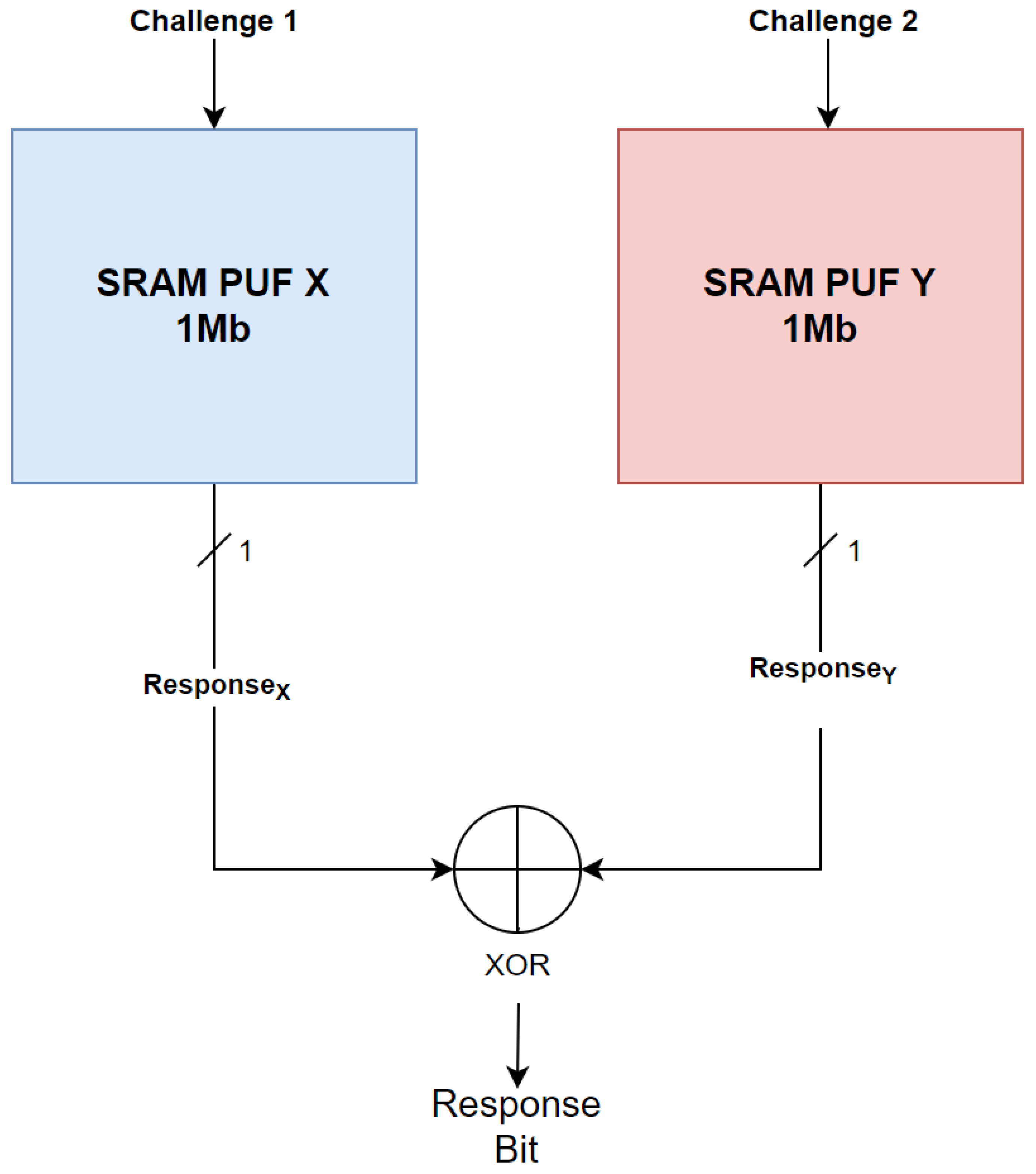
The SRAM PUF design incorporates two separate SRAM devices and a Boolean XOR gate. In this design, each SRAM device generates its response, and these responses are combined using the XOR gate to generate a single bit. This approach substantially increases the number of available CRPs from the original count of (representing the number of SRAM cells in each device) to . Consequently, this significant increase in the number of CRPs greatly enhances the entropy of the PUF. The SRAM XOR gate was added through software. The responses of both SRAMs are read and then XORed through software to generate the final response. The SRAM PUF XOR design is visually represented in Figure 3.

Figure 3.
SRAM XOR design. For each response bit, the two 1Mb SRAM PUFs receive a respective challenge and produce their respective responses. Both single-bit responses are then XORed together to produce the final combined response.
3.2. Hardware
In our implementation, we utilized ISSI IS64WV6416BLL SRAM chips as the SRAM devices (Integrated Silicon Solution Inc., Milpitas, CA, USA). These chips feature words of high-speed CMOS SRAM (Alliance Memory, Kirkland, WA, USA) and operate at 3.3 V logic, with access times as low as 12 ns. They exhibit low power consumption and are available in 44-pin packages. To interface with these devices, we designed custom PCB socket adapters that allow for the easy interchange of different SRAM chips. These SRAM chips were chosen for their ease of interfacing, widespread adoption, and availability, making them suitable for integration into any PUF design. A figure of these devices and adapters can be found in Figure 4.
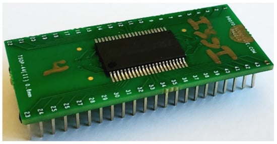
Figure 4.
The ISSI SRAM device on a custom PCB adapter. The PCB adapter breaks out each pin to a more accessible location. This adapter can be placed into a slot on the custom PCB.
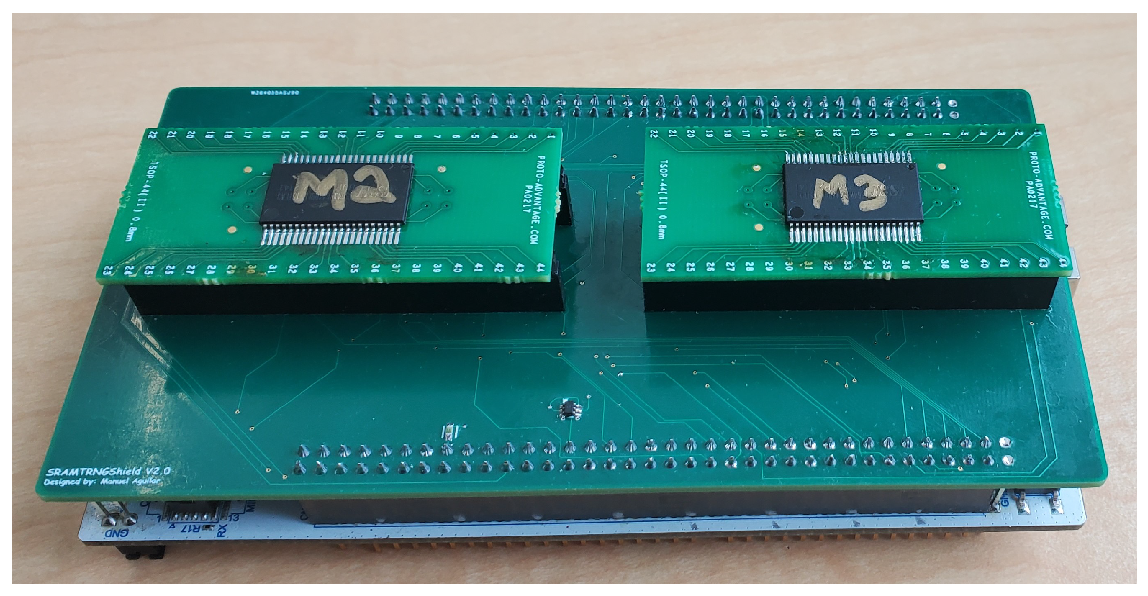
We implemented the SRAM XOR PUF on a low-power client using a custom-printed circuit board (PCB). The client device we used was the Nucleo-144 H743ZI2 developer kit (STMicroelectronics, Geneva, Switzerland). We used the custom PCB to interface with the SRAM devices, and the PCB included an integrated circuit switch for power cycling the device. A figure of the client device, custom PCB, and SRAM can be found in Figure 5.

Figure 5.
The Nucleo-144 developer kit, custom PCB, and SRAM devices 2 and 3. Each adapter is slotted into the PCB. The single small IC on the board allows control of the power to both SRAM chips. The sides of the PCB match the pin-out of the Nucleo development kit, allowing programmatic control.
4. Results
To perform an electrical characterization of the SRAM XOR design, we examined the behavior of the SRAM devices and SRAM cells, specifically focusing on their responses after each power cycle. We also focused on measuring the key properties that define a PUF, namely, reliability, uniqueness, and randomness. These properties were evaluated using specific metrics: BER for reliability, inter-chip Hamming Distance for uniqueness, and entropy for randomness. By calculating these metrics, we gained quantitative insights into the performance and security aspects of the SRAM XOR design.
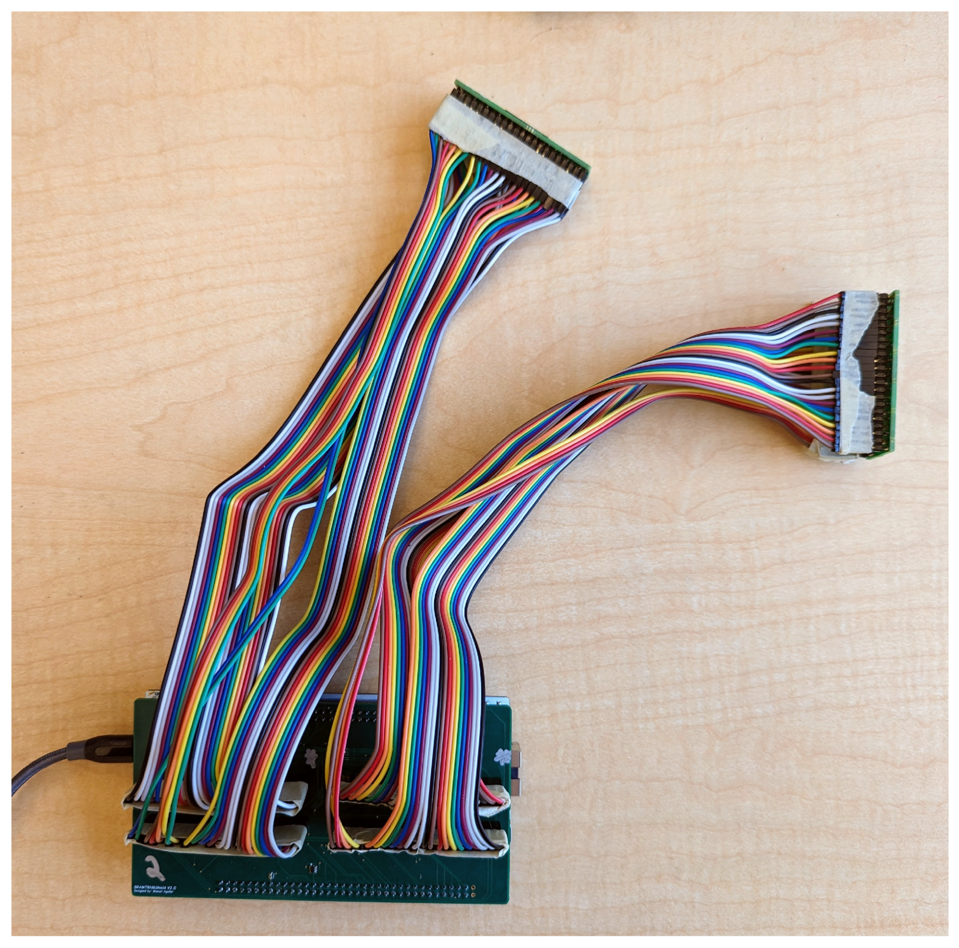
In addition, we conducted the tests across various temperature ranges: 0 °C, 23 °C, and 80 °C. To perform temperature testing, we employed the Associated Environmental Systems SD-501 temperature chamber. This chamber offers a broad temperature range, from −37 °C to 180 °C, allowing us to create diverse temperature conditions. To ensure an accurate assessment of the SRAM devices and eliminate any potential influence from external measurement circuitry, we used General-Purpose Input/Output (GPIO) pin jumper cables during the temperature tests. These measures helped isolate the impact of temperature on the devices under evaluation. A picture of the SRAM devices and jumper cables is found in Figure 6.

Figure 6.
An SRAM device connected to the client device using standard GPIO jumper cables for thermal testing.
4.1. Enrollment
The enrollment process is performed before generating CRPs from the PUF, where every possible CRP is generated and recorded in a database. It is a critical step, as the database is used to authenticate the responses of the physical PUF and locate the stable cells. For SRAM, the process involves reading out the entire contents of the SRAM device and power cycling the device. For a full enrollment and the achievement of a low BER, this process needs to happen approximately 1000 times.
4.1.1. Discharge Timings
One of the challenges encountered when implementing the SRAM PUF is the discharge time of the SRAM. This timing has implications for the enrollment process of SRAM, as it can influence the determination of stable and flaky cells. For instance, if a cell is initially read as a ‘1’ and then flips to a ‘0’ when read consecutively, there is a possibility of erroneously reading it as a ‘1’ before the cell fully discharges to ‘0’. To address this issue, it is necessary to introduce an adequate time gap between power cycles, allowing the energy from previous reads to dissipate and ensuring more accurate readings.
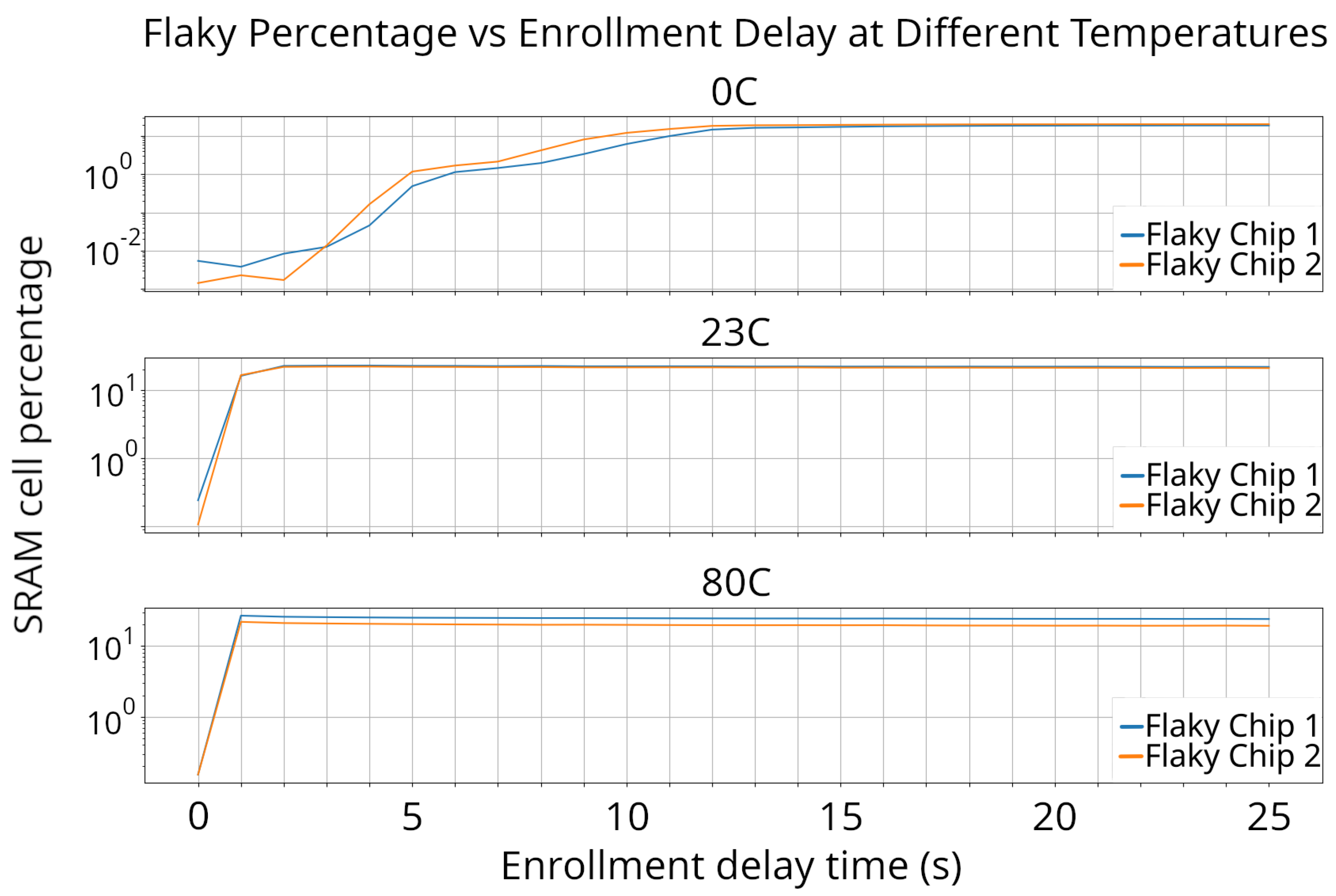
To investigate the impact of discharge on our SRAM devices, we enrolled the same devices using different power cycle times at various testing temperatures. We quantified the discharge time by analyzing the number of stable and flaky cells during each enrollment. It was expected that a shorter time interval between power cycles would result in less discharge time for each cell and for less flaky cells to be detected. The outcomes of these tests are presented in Figure 7.
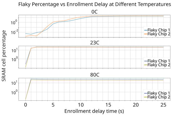
Figure 7.
Flakiness vs. enrollment delay time over different temperatures. The two flaky chips shown have no major differences in temperature or enrollment time. The SRAM chips used in this study use a similar enrollment cycle time of 1, 3, or 21 s since there is very little variation from chip to chip.
Upon analyzing Figure 7, we identified a significant pattern concerning SRAM enrollments, the time interval between power cycles, and different temperatures. At each temperature, we observed a sharp increase in the number of stable cells as the time between power cycles increased, reaching a specific threshold point that varies with each temperature. Beyond this threshold point, the number of detected flaky cells marginally decreased.
Enrollments conducted with almost zero seconds between power cycles demonstrated nearly no cell discharge, reducing the number of flaky cells detected. This phenomenon can be attributed to the charges trapped within each cell, where the cells retain information from previous reads, making them less likely to change. As the charges trapped within the cell are assumed to diminish over time, it can be inferred that the number of flaky cells increases as the charge from previous reads dissipates. The objective is to use only stable cells in key generation, which implies that enrollments with a higher number of flaky cells detected will produce low-error-rate keys.
Observations of flaky cells at various temperatures provided valuable insights into the discharge timings of the ISSI SRAM chip. At a temperature of 0 °C, the number of flaky cells peaked after 21 s. At 23 °C, the peak occurred between 2 and 3 s, while at 80 °C, it was observed after just 1 s. These findings indicate that the dispersion of the cell charge takes longer at lower temperatures.
To accommodate these temperature-dependent characteristics, the enrollment process will be adapted to utilize different power cycle times. Specifically, at 0 °C, the power cycle time for enrollment will be set to 21 s. At 23 °C, it will be 3 s, and at 80 °C, it will be 1 s. By adjusting the power cycle times according to the temperature, the enrollment process can effectively address the discharge times and ensure reliable and accurate results.
4.1.2. Read Count
During the enrollment process, multiple measurements are taken to determine the stability of each cell. Stable cells are consistently represented by either ‘0’ or ‘1’, indicating that they contain either exclusively ‘0’s or ‘1’s over the 1000 read collection.
A crucial factor in BER and enrollment is the number of reads conducted. A read refers to a single measurement of each SRAM cell. Increasing the number of reads during enrollment lowers the chance of selecting a flaky cell in a final key, lowering the key’s BER. However, each additional read gives diminishing returns and does not provide significant benefits concerning the time required for enrollment.
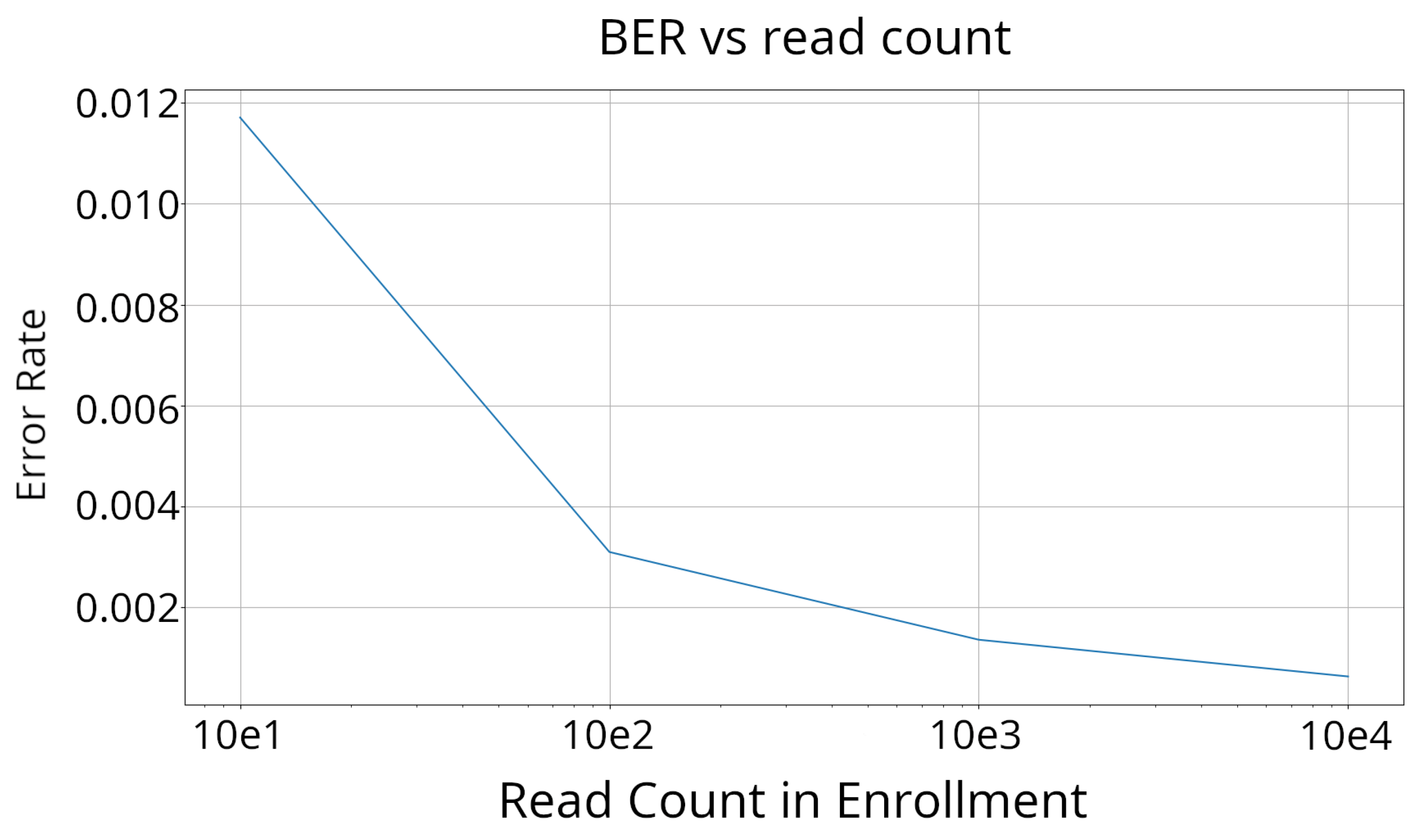
By increasing the number of reads, the likelihood of identifying a cell as flaky increases, resulting in a reduction in the number of stable cells available. To assess the impact of the read count, we conducted enrollments with progressively higher read counts. These enrollments were then used to generate a key, and the corresponding BER was measured. The results of this analysis are presented in Figure 8.
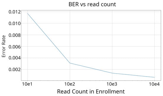
Figure 8.
BER vs. read count at 23 °C. As the enrollment count increases, the error rates within responses go down as well. This pattern follows a logarithmic decrease, and due to this, only 1000 enrollments are performed.
At a read count of 1000, the BER decreased to less than 1%. Given that error-correcting techniques such as error-correcting codes [32] and Response-Based Cryptography (RBC) [33] are capable of correcting such a low percentage of errors, a read count of 1000 was chosen for this research.
4.1.3. Quantifying Flakiness
The term ‘flaky’ is used to describe cells that do not exhibit exclusively a ‘0’ or ‘1’ state during the enrollment process. However, relying solely on this categorization does not provide an accurate measure of their flakiness. To quantify the flakiness of an SRAM device, we calculate the expected value for each cell. An expected value of 0 represents the most stable state, while an expected value of 0.50 represents the highest level of flakiness. This approach allows us to obtain a more comprehensive understanding of the flakiness of the SRAM device.
4.2. SRAM Device Characteristics
After enrolling ten SRAM devices, we examined their properties, particularly their flakiness and likelihood to represent either a ‘0’ or a ‘1’. To illustrate the characteristics of SRAM cells, we categorized all cells, regardless of their flakiness or stability, into five groups: strong/weak ‘1’s, strong/weak ’0’s, and super-flaky cells. Strong ’1’s are SRAM cells that exhibit a higher likelihood of being a ‘1’ when queried, only appearing as ‘1’ during enrollment. Strong ’0’s, on the other hand, are more inclined to represent a ‘0’ when queried and during enrollment, never appearing as a ‘1’. Super-flaky cells do not prefer either state and have an equal chance of being a ‘0’ or a ‘1’, indicated by showing up in the 4% range centered around the median count. Lastly, a cell is a weak ‘0’ or ‘1’ if it is not categorized into the other three categories and falls into its respective biasing. This categorization scheme helps visualize and differentiate the behavior and tendencies of SRAM cells.
In this study, we analyzed ten SRAM devices at each temperature and recorded their device characteristics in Table 2. Based on the information provided in the table, it can be inferred that the devices display a slight preference for one state over the other, reducing their overall entropy. According to the classifications used in this study, approximately one-third of the SRAM cells are categorized as ‘flaky’. Moreover, it is observed that the number of flaky cells tends to increase as the temperature rises.
Table 2.
SRAM cell population number of occurring ones over 1000 reads at 3 different temperatures. Characteristics include noise from the SRAM devices and the additional circuitry to access the cell and, as a result, are not characteristic of the devices themselves.
4.2.1. Temperature Effects
Temperature testing is essential for the comprehensive electrical characterization of SRAMs. Given that temperature variations can significantly affect the performance and reliability of electronic devices, it is crucial to evaluate the behavior of PUFs under varying thermal conditions.
To assess the robustness and reliability of the SRAM devices, we conducted thorough tests and characterizations at three distinct temperatures: 0 °C, 23 °C, and 80 °C. To isolate the impact of temperature on the SRAM devices and minimize the influence of external measurement circuitry, we employed flat flex cables and adapters during the temperature tests. This approach enabled us to focus solely on the thermal effects on the SRAM, providing a clear understanding of its isolated thermal behavior.
We utilized the Associated Environmental Systems SD-501 temperature chamber to create a wide range of temperature conditions, spanning from −37 °C to 180 °C. By examining the behavior of the PUFs across this temperature range, we aimed to gain insights into the effects of temperature variations on their reliability. This knowledge will facilitate informed decisions.
The temperature significantly affects the classification of SRAM cells, determining whether they are classified as strong/weak ‘1’s, ‘0’s, or ‘flaky’. On average, there was a 10.09% difference in SRAM cell classification between enrollments conducted at 0 °C and enrollments conducted at 23 °C. Similarly, the difference in classification between enrollments conducted at 23 °C and enrollments conducted at 80 °C was 18.66%. Notably, the difference in classification between enrollments conducted at 0 °C and enrollments conducted at 80 °C was 34.10%. However, even stable cells exhibited a relatively small but still significant change in cell type (strong ‘0’, ‘1’, or super-flaky). On average, there was a 0.26% difference in SRAM cell type between enrollments conducted at 0 °C and enrollments conducted at 23 °C. Similarly, the difference in cell type between enrollments conducted at 23 °C and enrollments conducted at 80 °C was 2.91%. Notably, the difference between enrollments conducted at 0 °C and enrollments conducted at 80 °C was 13.52%. These results correlate with increased thermal noise, affecting the stability of each cell.
A heatmap illustrating the change between temperatures in a subsection of an SRAM device’s enrollment can be seen in Figure 9.

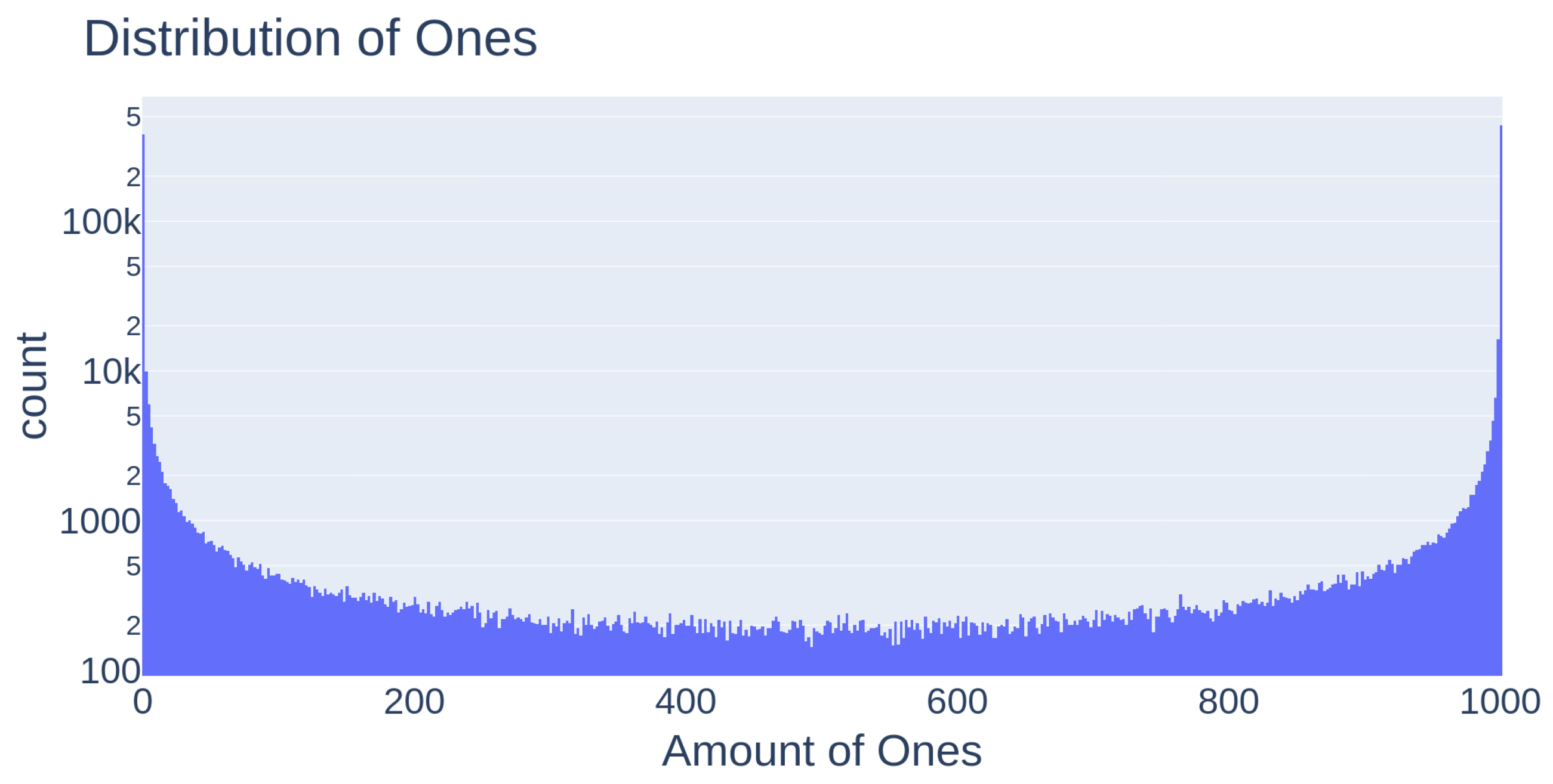
Figure 9.
Log-scale histogram of cell response population. As can be seen, most cells fall into a very stable response pattern, with very few in the middle with high unpredictability.
4.2.2. Patterns
In an SRAM device, even if the responses have an equal number of ‘1’s and ‘0’s, there may still be unexpected patterns present in the SRAM cells that can impact the security and randomness of the PUF. The SRAM chips used in this study, specifically the ISSI IS64WV6416BLL SRAM chips, are organized into 65,536 words, each containing 16 bits. To ensure the absence of repeating patterns, a heatmap was generated to visualize the state of each SRAM cell for each SRAM device.
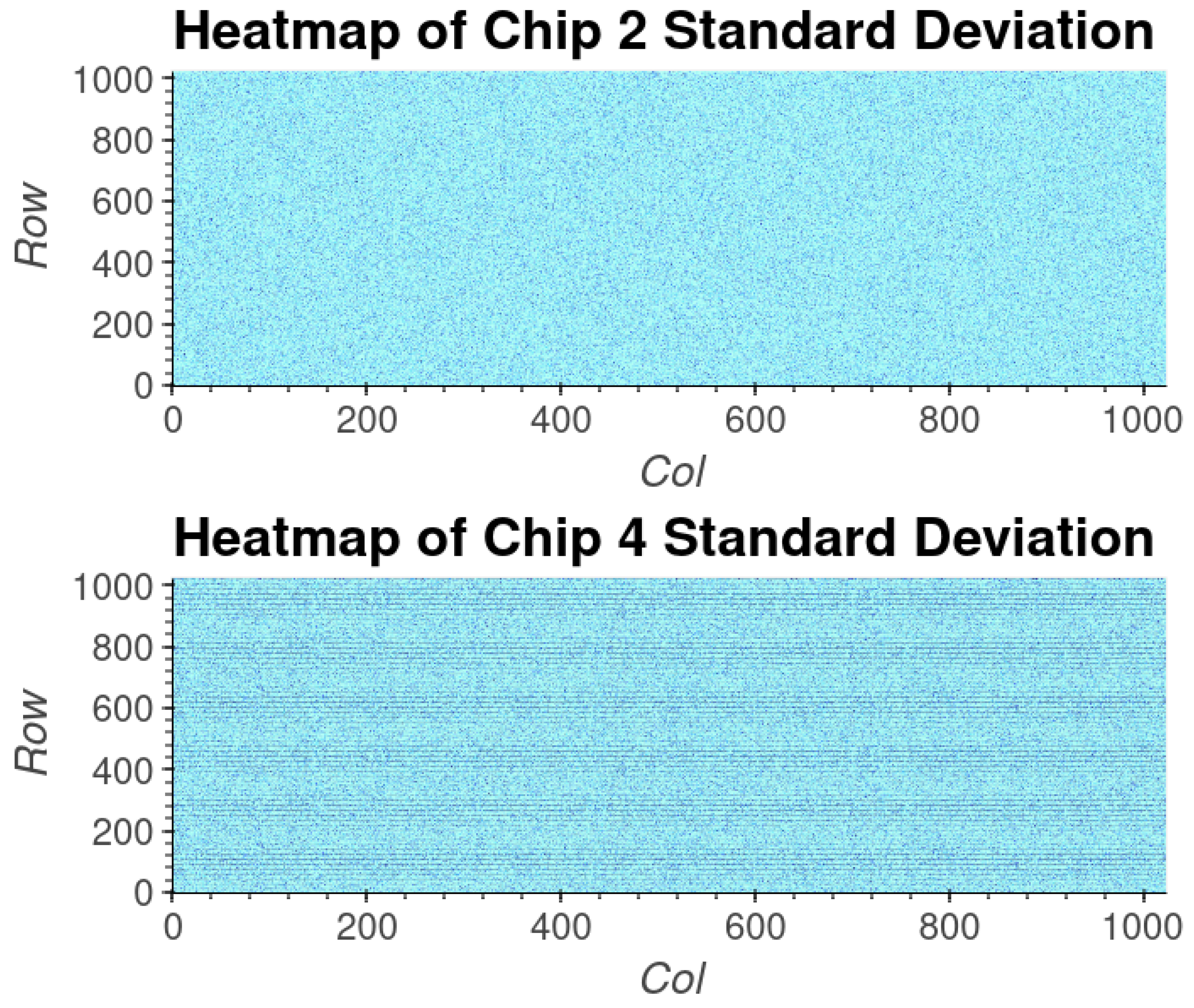
Upon examining the heatmaps, patterns can be seen occurring with temperature; as such, each SRAM needs to be independently verified to avoid any temperature-dependent patterns. A heatmap of several SRAM chips can be seen in Figure 10. A likely cause of the vertical striations is internal cell read-out circuity that causes biasing at different temperatures.
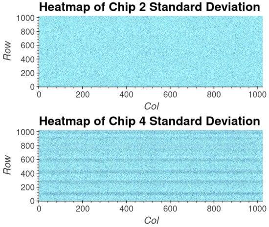
Figure 10.
A heatmap of the cell response’s standard deviation of the calculated temperature. The cell’s standard deviation across all three temperatures was calculated to present a pixel in the heatmap. The standard deviation shows a striation pattern for chip 4; however, this pattern does not appear in the mean response. Before use as a PUF, the SRAM needs to be tested for any patterning within the chip.
4.2.3. Uniformity
Ensuring consistency in a PUF involves generating responses with an equal distribution of ‘1’s and ‘0’s. However, there is no dedicated universal function specifically designed to assess uniformity in a PUF. Instead, uniformity serves as a general metric that describes the ratio of ‘1’s to ‘0’s in the PUF system’s responses. Although individual SRAM devices may exhibit a slight preference toward ‘1’s in their responses, the overall responses from the entire system can vary.
In the case of a binary PUF, an ideal occurrence of ‘1’s would be 50%. To evaluate and quantify the level of uniformity, a key comprising one million bits was generated at different temperatures, with flaky bits being filtered out. The percentage of ‘1’s in the generated key was then calculated. At each temperature, the percentage of ‘1’s ranged from 49.85% to 50.00%, indicating that the responses’ uniformity is very close to the ideal target. However, there is a slight bias toward ‘0’s, which leads to a reduction in the entropy of the responses.
4.3. PUF Metrics
To assess the randomness, uniqueness, and reliability of the PUF design, we calculated three key metrics: entropy, inter-chip distance, and BER. These metrics were used as quantitative measures to evaluate the performance and characteristics of the PUF design.
4.3.1. Entropy
To assess the entropy of our PUF design, we employed the Shannon entropy formula, which can be referenced as Equation (1) as is used in [34]. This formula allows us to quantify the correlation among the bits in the responses obtained from our PUF design. In the given equation, the variable represents the probability of a random variable X having the value x. The logarithm, typically taken to the base-2 , is used to quantify entropy in terms of bits.
The Shannon entropy has a minimum value of zero, indicating that the input lacks randomness or variability, while its maximum value is , where n represents the number of possible inputs. In this case, since the input is a binary sequence (with two possible inputs, 0 and 1), n equals 2, and thus, the upper bound of the entropy per bit is 1. This signifies that the input demonstrates maximum randomness or unpredictability.
The client device generated 1000 keys consisting of 500 bits at different temperatures. Subsequently, the entropy of each key was determined and averaged together. Specifically, at temperatures of 0 °C, 23 °C, and 80 °C, the entropy was found to be 0.9999 per bit.
These results indicate that the entropy remains consistently high across different temperatures. Therefore, the temperature variations have minimal influence on the entropy.
4.3.2. Uniqueness
To assess the uniqueness of the PUF, the (see Section 2.2) was calculated using five different configurations of the SRAM XOR PUF. Both filtered and unfiltered CRPs were used to compute the for each of the five configurations. The final value was obtained by averaging the results. Filtered CRPs were obtained by excluding flaky cells, while unfiltered CRPs included all cells. The testing was conducted at various temperatures, and the results are shown in Table 3.
Table 3.
The average over 5 different SRAM XOR PUF pairings. With very little variation with temperature and filtering, the is not heavily affected by temperature or filtering.
These findings demonstrate the impressive uniqueness metrics of the SRAM PUF design and devices. The values are consistently close to the ideal value of 50%, indicating high uniqueness. Importantly, these metrics remain consistent and are not significantly affected by temperature variations or filtering.
4.3.3. Bit-Error Rate
The BER is a metric used to assess the reliability of a PUF. It involves generating a sequence of responses on the client device by applying a set of challenges and comparing it to the one generated on the server side using the same set of challenges. The server utilizes enrollment data to generate responses, while the client generates real-time responses using the PUF. The BER is determined by calculating the number of discrepancies between the two response sequences and dividing it by the size of the response sequence.
In essence, the BER is analogous to the intra-chip Hamming Distance () in that they both measure the reliability of a PUF. The BER compares the response of a PUF to the response generated from the enrollment data. However, the describes the average expected difference between two PUF responses obtained using the same PUF and the same challenge.
To evaluate the BER of the proposed design, enrollments were conducted at three different temperatures: 0 °C, 23 °C, and 80 °C. The SRAM XOR PUF was subsequently tested at each temperature using the enrollments obtained at all three temperature settings.
In each test, a key consisting of one million bits was generated by utilizing the physical SRAM devices on the client side and the enrollment information on the server side. To assess the quality of the generated keys, the Hamming Distance between the two keys was calculated. This distance measurement was then divided by the total size of the key to determine the BER. The results of the BER tests can be found in Table 4.
Table 4.
The BER of a 1-million-bit-long key at different temperatures when using enrollments taken at varying temperatures. Each key used for BER measurement was 1 million bits long.
The BER results show low error when using the appropriate enrollment, maintaining a BER below 1% when using the ideal enrollments. The BER does get worse when non-matching enrollments are used, reaching as high as 10%.
5. Discussion
This research presents a novel SRAM-based PUF design that addresses several limitations of previous designs while maintaining the simplicity and accessibility of SRAM devices. The proposed PUF utilizes two SRAM devices in conjunction with an XOR gate. To evaluate its performance, ten ISSI IS64WV6416BLL SRAM chips were tested at three different temperatures: 0 °C, 23 °C, and 80 °C. To ensure accurate measurements, GPIO jumper cables were employed to isolate the SRAM devices from external circuitry and mitigate any thermal influences.
A notable limitation of this study is the small sample size of SRAM devices tested. With only ten SRAM devices included, the sample size may not provide sufficient statistical significance for the results. Future research should involve a larger number of SRAM devices to enhance the robustness of the findings.
The PUF was evaluated based on three metrics: bit-error rate (BER), inter-bit Hamming Distance (), and entropy. The results demonstrated impressive BER performance, with an average BER of 0.2% at the temperature at which it was initially enrolled. However, the average BER increased to approximately 10% where the temperature was furthest from the temperature during enrollment. The increase in BER likely comes from cells that become flaky at different temperatures. When the wrong temperature enrollment is used, some flaky cells may not be detected and may therefore be masked. If temperature is not properly accounted for, the BER is still low enough to allow for correction by ECC or RBC. However, at more extreme values of enrollment and challenge, the BER may become large enough to cause false rejections during authentication, rejecting a valid user. This downside can be mitigated by using multi-temperature enrollment, where a flaky cell at any temperature is masked away during selection. On top of a low BER, the design exhibited a high value of 0.4966 and a substantial entropy of 0.9982.
Compared to previous SRAM PUF implementations, the SRAM XOR PUF showed superior performance. While the Microcontroller SRAM PUF achieved a lower BER, the SRAM XOR PUF performed equally or even better in other metrics. A detailed comparison of the PUF metrics between the SRAM XOR design and previous designs can be found in Table 5.
Table 5.
PUF metrics of previously implemented SRAM PUFs compared to the new design. The term n denotes the number of SRAM cells on the device. Moreover, work in [22,26] used fuzzy extractors, a mix of filtering fuzzy cells and error correction code, to improve reliability. The SRAM XOR PUF used fuzzy extractors by just filtering out fuzzy cells.
Moreover, the number of CRPs for our PUF was significantly higher than that for other PUFs. This increased number enhances security by making it more difficult for an attacker to reliably clone the PUF within a short time frame if they have limited-time access to the PUF’s challenges and responses. Additionally, a higher number of CRPs provides improved protection against eavesdropping attacks, in which an attacker may attempt to exploit previously known CRPs to reconstruct parts of the authentication key [4]. However, the increase in CRPs comes at the cost of response reliability, which is decreased by approximately 50%. This decline occurs because if just one of the SRAM bits is unreliable, it can render the entire response unreliable.
However, a notable drawback was observed in the SRAM devices, specifically the non-uniform distribution of ‘1’s and patterns unique to individual SRAM devices. This device vulnerability poses a potential security risk to the overall PUF design. These observed patterns may stem from the manufacturing process, prolonged device usage, or influences from the measurement circuitry, such as the adapter, GPIO jumper cables, or testing equipment. Therefore, these factors could affect the practicality of using the SRAM device as a PUF in certain applications, as different circuits in the field may access the SRAM cells differently. However, due to two different die being XORed together, the patterning is greatly diminished with the interaction between the unique patterns in each SRAM. As a matter of precaution, SRAM pairs need to be validated to not have an existing pattern before being used as an SRAM XOR PUF.
Future Work
Further research is essential to investigate the effects of aging on this design and to develop potential mitigation strategies. Although our design enhances the uniqueness, randomness, and security of the SRAM PUF by employing multiple challenge–response pairs (CRPs), a critical challenge remains: the susceptibility of SRAM PUFs to aging. This phenomenon can significantly impact the stability and reproducibility of PUF outputs. Therefore, a comprehensive examination of the aging effects on this dual-SRAM architecture is necessary, as the integration of responses from two SRAM components may intensify the reliability issues typically associated with aging. Potential avenues for future research include employing accelerated aging methods [35,36] to assess their impact on the responses generated by our design.
Additionally, the inclusion of two SRAM components within the same architecture presents a drawback. A more effective design could involve utilizing a single SRAM that captures multiple samples per challenge. By XORing these samples together, a single-bit response can be generated that emulates the results of two SRAM reads followed by XORing, as demonstrated in this paper. While a sample size of two effectively represents the findings of this study, this approach can be scaled to accommodate any number of samples, provided that care is taken to avoid repeating challenge addresses, as repetition would negate their contribution in the XOR operation. Additionally, this design can be implemented entirely in software, facilitating an exponential increase in the potential challenges derived from the existing SRAM. Consequently, this method could enable any currently utilized SRAM PUF hardware to adapt to a framework similar to the XOR SRAM PUF, significantly enhancing the randomness and the number of possible CRPs generated.
Author Contributions
J.G. contributed software, data collection/analysis, writing, and revising. M.A.R. contributed hardware design/creation, visualizations, and tables. B.C. supervised the research. All authors have read and agreed to the published version of the manuscript.
Funding
This research received no external funding.
Institutional Review Board Statement
Not applicable.
Informed Consent Statement
Not applicable.
Data Availability Statement
Data available in a publicly accessible repository: https://github.com/NAU-Cybersecurity-lab/xor-sram-data, accessed on 16 October 2024.
Conflicts of Interest
The authors declare no conflicts of interest.
Abbreviations
The following abbreviations are used in this manuscript:
| AES | Advanced Encryption Standards |
| BER | Bit-error rate |
| CRP | Challenge–response pair |
| GPIO | General-Purpose Input/Output |
| SRAM | Static Random-Access Memory |
| PCB | Printed circuit board |
| PUF | Physically Unclonable Function |
| RBC | Response-Based Cryptography |
| RSA | Rivest–Shamir–Adleman |
| XOR | Exclusive-OR |
References
- Anderson, R.; Kuhn, M. Tamper resistance-a cautionary note. In Proceedings of the Second Usenix Workshop on Electronic Commerce, Oakland, CA, USA, 18–21 November 1996; Volume 2, pp. 1–11. [Google Scholar]
- Anderson, R.; Kuhn, M. Low cost attacks on tamper resistant devices. In Proceedings of the International Workshop on Security Protocols, Paris, France, 7–9 April 1997; pp. 125–136. [Google Scholar]
- Guajardo, J.; Kumar, S.S.; Schrijen, G.J.; Tuyls, P. FPGA intrinsic PUFs and their use for IP protection. In Proceedings of the International Workshop on Cryptographic Hardware and Embedded Systems, Vienna, Austria, 10–13 September 2007; pp. 63–80. [Google Scholar]
- McGrath, T.; Bagci, I.E.; Wang, Z.M.; Roedig, U.; Young, R.J. A puf taxonomy. Appl. Phys. Rev. 2019, 6, 011303. [Google Scholar] [CrossRef]
- Lorenz, D.; Georgakos, G.; Schlichtmann, U. Aging analysis of circuit timing considering NBTI and HCI. In Proceedings of the 2009 15th IEEE International On-Line Testing Symposium, Lisbon, Portugal, 24–26 June 2009; pp. 3–8. [Google Scholar]
- Bhatta, N.; Singh, H.; Ghimire, A.; Amsaad, F. Analyzing Aging Effects on SRAM PUFs: Implications for Security and Reliability. J. Hardw. Syst. Secur. 2024, 1–13. [Google Scholar] [CrossRef]
- Holcomb, D.E.; Burleson, W.P.; Fu, K. Initial SRAM State as a Fingerprint and Source of True Random Numbers for RFID Tags. In Proceedings of the Conference on RFID Security, 2007, Volume 7, p. 1. Available online: https://web.eecs.umich.edu/~kevinfu/papers/holcomb-FERNS-RFIDSec07.pdf (accessed on 13 June 2024).
- yubico. OTPs Explained. Available online: https://developers.yubico.com/OTP/OTPs_Explained.html (accessed on 16 October 2024).
- Gassend, B.; Clarke, D.; Van Dijk, M.; Devadas, S. Silicon physical random functions. In Proceedings of the 9th ACM Conference on Computer and Communications Security, Washington, DC, USA, 18–22 November 2002; pp. 148–160. [Google Scholar]
- Simmons, G.J. A system for verifying user identity and authorization at the point-of sale or access. Cryptologia 1984, 8, 1–21. [Google Scholar] [CrossRef]
- Thompson, A. An evolved circuit, intrinsic in silicon, entwined with physics. In Proceedings of the International Conference on Evolvable Systems, Berlin/Heidelberg, Germany, 7–8 October 1996; pp. 390–405. [Google Scholar]
- Gassend, B.L.P. Physical Random Functions. Ph.D. Thesis, Massachusetts Institute of Technology, Cambridge, MA, USA, 2003. [Google Scholar]
- Suh, G.E.; Devadas, S. Physical unclonable functions for device authentication and secret key generation. In Proceedings of the 2007 44th ACM/IEEE Design Automation Conference, San Diego, CA, USA, 4–8 June 2007; pp. 9–14. [Google Scholar]
- Phyo Aung, P.; Mashiko, K.; Ismail, N.; Ooi, C.Y. Evaluation of SRAM PUF Characteristics and Generation of Stable Bits for IoT Security. In Emerging Trends in Intelligent Computing and Informatics: Data Science, Intelligent Information Systems and Smart Computing; Springer International Publishing: Berlin/Heidelberg, Germany, 2020; pp. 441–450. [Google Scholar] [CrossRef]
- Rose, G.S.; Meade, C.A. Performance analysis of a memristive crossbar PUF design. In Proceedings of the 2015 52nd ACM/EDAC/IEEE Design Automation Conference (DAC), San Francisco, CA, USA, 8 June 2015; pp. 1–6. [Google Scholar]
- Wilson, T.; Cambou, B. Tamper-sensitive pre-formed ReRAM-based PUFs: Methods and Experimental Validation. Front. Nanotechnol. 2022, 4, 1055545. [Google Scholar] [CrossRef]
- Wilson, T.; Jain, S.; Garrard, J.; Cambou, B.; Burke, I. Characterization of ReRAM Arrays Operating in the Pre-formed Range to Design Reliable PUFs. In Proceedings of the Intelligent Computing; Arai, K., Ed.; Springer: Cham, Switzerland, 2024; pp. 328–350. [Google Scholar]
- Zhang, L.; Fong, X.; Chang, C.H.; Kong, Z.H.; Roy, K. Highly reliable memory-based physical unclonable function using spin-transfer torque MRAM. In Proceedings of the 2014 IEEE International Symposium on Circuits and Systems (ISCAS), Melbourne, VIC, Australia, 1–5 June 2014; pp. 2169–2172. [Google Scholar]
- Lim, S.; Song, B.; Jung, S.O. Highly independent MTJ-based PUF system using diode-connected transistor and two-step postprocessing for improved response stability. IEEE Trans. Inf. Forensics Secur. 2020, 15, 2798–2807. [Google Scholar] [CrossRef]
- Roel, M. Physically Unclonable Functions: Constructions, Properties and Applications; Katholieke Universiteit Leuven: Leuven, Belgium, 2012. [Google Scholar]
- Holcomb, D.E.; Burleson, W.P.; Fu, K. Power-up SRAM state as an identifying fingerprint and source of true random numbers. IEEE Trans. Comput. 2008, 58, 1198–1210. [Google Scholar] [CrossRef]
- Böhm, C.; Hofer, M.; Pribyl, W. A microcontroller sram-puf. In Proceedings of the 2011 5th International Conference on Network and System Security, Milan, Italy, 6–8 September 2011; pp. 269–273. [Google Scholar]
- Wilde, F. Large scale characterization of SRAM on Infineon XMC microcontrollers as PUF. In Proceedings of the Fourth Workshop on Cryptography and Security in Computing Systems, Stockholm, Sweden, 24 January 2017; pp. 13–18. [Google Scholar]
- Roelke, A.; Stan, M.R. Attacking an SRAM-based PUF through Wearout. In Proceedings of the 2016 IEEE Computer Society Annual Symposium on VLSI (ISVLSI), Pittsburgh, PA, USA, 11–13 July 2016; pp. 206–211. [Google Scholar]
- Garg, A.; Kim, T.T. Design of SRAM PUF with improved uniformity and reliability utilizing device aging effect. In Proceedings of the 2014 IEEE International Symposium on Circuits and Systems (ISCAS), Melbourne, VIC, Australia, 1–5 June 2014; pp. 1941–1944. [Google Scholar]
- Baek, S.; Yu, G.H.; Kim, J.; Ngo, C.T.; Eshraghian, J.K.; Hong, J.P. A reconfigurable SRAM based CMOS PUF with challenge to response pairs. IEEE Access 2021, 9, 79947–79960. [Google Scholar] [CrossRef]
- Faour, S.; Korecic, B.; Vučinić, M.; Maksimovic, F.; Burnett, D.C.; Muhlethaler, P.; Watteyne, T. Single-Chip Motes and SRAM PUF: Feasibility Study. In Proceedings of the 2024 IEEE Workshop on Crystal-Free/-Less Radio and System-Based Research for IoT (CrystalFreeIoT), Hong Kong, China, 14 May 2024. [Google Scholar]
- Herder, C.; Yu, M.D.; Koushanfar, F.; Devadas, S. Physical unclonable functions and applications: A tutorial. Proc. IEEE 2014, 102, 1126–1141. [Google Scholar] [CrossRef]
- Yehoshuva, C.; Raja Adhithan, R.; Nalla Anandakumar, N. A survey of security attacks on silicon based weak PUF architectures. In Proceedings of the Security in Computing and Communications: 8th International Symposium, SSCC 2020, Chennai, India, 14–17 October 2020; Revised Selected Papers 8. pp. 107–122. [Google Scholar]
- Nedospasov, D.; Seifert, J.P.; Helfmeier, C.; Boit, C. Invasive PUF analysis. In Proceedings of the 2013 Workshop on Fault Diagnosis and Tolerance in Cryptography, Los Alamitos, CA, USA, 20 August 2013; pp. 30–38. [Google Scholar]
- Al-Meer, A.; Al-Kuwari, S. Physical unclonable functions (PUF) for IoT devices. ACM Comput. Surv. 2023, 55, 1–31. [Google Scholar] [CrossRef]
- Dodis, Y.; Reyzin, L.; Smith, A. Fuzzy extractors: How to generate strong keys from biometrics and other noisy data. In Proceedings of the International Conference on the Theory and Applications of Cryptographic Techniques, Interlaken, Switzerland, 2–6 May 2004; pp. 523–540. [Google Scholar]
- Cambou, B.; Philabaum, C.; Booher, D.; Telesca, D.A. Response-based cryptographic methods with ternary physical unclonable functions. In Proceedings of the Advances in Information and Communication: Proceedings of the 2019 Future of Information and Communication Conference (FICC); Springer International Publishing: Berlin/Heidelberg, Germany, 2020; Volume 2, pp. 781–800. [Google Scholar]
- Maes, R.; Van Herrewege, A.; Verbauwhede, I. PUFKY: A fully functional PUF-based cryptographic key generator. In Proceedings of the Cryptographic Hardware and Embedded Systems–CHES 2012: 14th International Workshop, Leuven, Belgium, 9–12 September 2012; pp. 302–319. [Google Scholar]
- Wang, R.; Selimis, G.; Maes, R.; Goossens, S. Long-term continuous assessment of SRAM PUF and source of random numbers. In Proceedings of the 2020 Design, Automation & Test in Europe Conference & Exhibition (DATE), Grenoble, France, 9–13 March 2020; pp. 7–12. [Google Scholar]
- Bhatta, N.P.; Singh, H.; Ghimire, A.; Rahman, M.T.; Amsaad, F. Aging of SRAM PUFs: Mitigation and Advancements Through Machine Learning Techniques. In Proceedings of the 2023 IEEE Physical Assurance and Inspection of Electronics (PAINE), Huntsville, AL, USA, 24–26 October 2023; pp. 1–6. [Google Scholar]

Disclaimer/Publisher’s Note: The statements, opinions and data contained in all publications are solely those of the individual author(s) and contributor(s) and not of MDPI and/or the editor(s). MDPI and/or the editor(s) disclaim responsibility for any injury to people or property resulting from any ideas, methods, instructions or products referred to in the content. |
© 2024 by the authors. Licensee MDPI, Basel, Switzerland. This article is an open access article distributed under the terms and conditions of the Creative Commons Attribution (CC BY) license (https://creativecommons.org/licenses/by/4.0/).