Abstract
Most electronic devices are susceptible to electromagnetic interference (EMI); thus, it is necessary to recognize and identify the cause and effect of EMI as it can corrupt electronic signals and degrade equipment performance. Particularly, in semiconductor manufacturing, the equipment used for image capturing is subject to various noises induced by EMI, causing the image analysis to be unreliable during the image recognition and digitization process. Thus, in this research, we aim to detect and quantify the influence of EMI on semiconductor SEM (scanning electron microscope) images. For this, we apply several useful denoising and edge detection techniques to find a clearer distorted shape from EMI-generated images and then compute five shape-related measures to evaluate the distortion. From a comprehensive experimental analysis and statistical tests, it is found that the medians of all the extracted shape-related measures of high-EMI SEM images are higher than those of both medium- and weak-EMI SEM images, and also all the p-values of the statistical tests are close to 0, and thus we can conclude that all the measures are good quantification metrics for assessing the impact of EMI on semiconductor SEM images.
1. Introduction
Image distortion caused by electromagnetic interference (EMI) that interferes with the performance of electrical equipment is a very critical problem in various precision research applications [1]. Particularly in semiconductor manufacturing, to detect and classify various defects on wafers, many automatic defect classification (ADC) methods have been developed [2,3]. In recent years, a variety of machine learning and deep learning techniques using SEM image data have been applied to defect detection and classification tasks in diverse areas, including semiconductor manufacturing [4,5,6,7,8,9,10,11,12,13,14,15,16,17]. Nakagaki et al. (2009) proposed a novel recognition technique for defect areas on semiconductor wafers using SEM images [18]. O’Leary et al. (2020) investigated a deep convolutional neural network (CNN) for defect classification using SEM images and energy-dispersive X-ray (EDX) spectroscopy data [7]. de la Rosa et al. (2021) presented a review of the defect detection and classification in semiconductor processes using machine learning and deep learning approaches combined with SEM images [13]. Liang et al. (2022) proposed an efficient method for processing the low-quality image data of integrated circuits to provide fundamental data for verification tasks [16]. Gómez-Sirvent et al. (2022) used the bag of visual words (BoVW) and Fisher vector (FV) coding methods for semiconductor wafer defect classification using SEM images [15]. Nam et al. (2022) proposed a generative adversarial network (GAN) that enables precise pattern alignment by transforming SEM images into target-like computer-aided design (CAD) images [17]. However, most previous research focused on defect detection and classification in semiconductor wafers but not on the identification and quantification of the distortion degree of EMI-contaminated SEM images. Thus, in this research, we consider several denoising and edge detection algorithms and then extract five measures (i.e., image object area, image object contour, rectangular area of the image object, extend index, and solidity index) to quantify the image distortion caused by EMI in semiconductor SEM images. To select the best denoising and edge detection techniques, we considered two evaluation metrics, that is, the mean squared error (MSE) for denoising and classification accuracy for edge detection techniques. The rest of this article is organized as follows. The literature reviews of EMI analysis, denoising algorithms, and edge detection algorithms are presented in Section 2. The details of the proposed approach and both experimental framework and analysis results are given in Section 3 and Section 4, respectively. Finally, the conclusions and some future research directions are discussed in Section 5.
2. Related Works
2.1. EMI Analysis
Electron microscopy is the most commonly used analytical inspection tool in semiconductor manufacturing with equipment. Particularly, in the semiconductor defect analysis, we can easily find that the device images such as scanning electron microscope (SEM) and transmission electron microscope (TEM) are distorted by several external or internal image distortion sources, such as electromagnetic interference (EMI), which is the disturbance induced by an electromagnetic field that interferes with the performance of electrical equipment. EMI is a common cause of many problems in precision research applications. Usually, distortions of image objects on SEM images due to EMI are visible as edge blur or vibration. To reduce the influence of EMI, hardware solutions such as electrostatic and magnetic shielding can be used, but in some cases, these protective measures are very expensive and considerably difficult to implement. Another approach is to use digital image processing to perform image distortion correction. Płuska et al. (2006) presented a median filtering combined with the scan-line shift correction method for eliminating the periodic distortions from SEM images [19]. Płuska et al. (2009) presented a method for separating various causes of SEM image distortions generated by EMI and relating the causes to certain elements of the SEM system to select optimal solutions for distortion reduction [1]. Ning et al. (2018) analyzed the influence of scanning distortion on STEM images in both real and reciprocal spaces by modeling and simulations [20]. Pradelles et al. (2021) proposed a dedicated edge detection algorithm to measure the line edge roughness (LER) of 2D curvilinear patterns on CD-SEM images [21]. Weisbuch et al. (2021) presented a method to evaluate and optimize the CD (critical dimension) matching between a reference standard SEM-CD and SEM contours [22].
2.2. Denoising Algorithms
Due to the influence of many factors, such as environment and transmission channel, images can be contaminated by noises during their acquisition, compression, and transmission processes, thus leading to the loss and contamination of image information. Therefore, it is highly difficult to capture the exact shape of the image object due to various noises lowering the quality of the image. In various microscope systems, hardware-wise or software-based methods can be considered to remove noise or to protect the image information from noise. Since, in many cases, it is quite difficult to implement noise prevention hardware, digital denoising is considered the most effective alternative. Image denoising is to eliminate undesirable noise in an image so as to restore the true image. To improve image extraction capability by removing undesirable signals (i.e., noise), many useful denoising methods have been developed [23,24,25]. Denoising algorithms (also called noise filters) in image processing applications can be categorized into two types, i.e., linear filters and non-linear filters. In general, linear filters work effectively for normal or stationary pixels in an image, but they may not work well for non-stationary pixels (e.g., edges or corners or sudden bumps). To compensate for this, several non-linear filters for removing noises in images have been developed [26,27], for example, bilateral filter, median filter, non-local means (NLM) filter, etc. However, most of these noise filters use only local data, which only contain partial information around the pixel of interest; therefore, an object’s edges on the image could be blurred or distorted [28,29,30,31]. As one of the linear smoothing methods, the Gaussian filter has been developed based on the fact that the image slowly changes spatially, that is, neighboring pixels have similar values. However, the performance in rapidly changing areas such as an edge (or outline or boundary) may decrease, and the shape of the detected edge can be somewhat unclear [30]. To maintain edge information while removing noise on other pixels in the image, the bilateral filter has been developed. The bilateral filter, which combines domain and range filtering, uses a weighted average of neighboring pixel values as a Gaussian filter. Here, the weight is calculated with the consideration of not only the Euclidean distance between the current pixel and the neighboring pixels but also radiometric differences (i.e., differences in color intensity and depth). The weight of a pixel and its neighbor , , is computed as follows:
where and are functions of the distance between pixels and the radiometric (i.e., color) difference between pixels, respectively. These functions can be defined using the following Gaussian function as follows:
where and are the parameters that control characteristics of spatial and radiometric weights, respectively. However, the bilateral filter has difficulty in reducing impulse noise, which is caused by sudden and sharp disturbances in the image signal [32]. To overcome this problem, the median filter has been developed. The median filter, for each pixel, arranges neighboring pixels in order according to the pixel value to obtain the median pixel value and then smooths the image by replacing the pixel value located at the center of the filter mask with the median pixel value. The two-dimensional median filter with window size is defined as follows:
where is the intensity value of the input image, and is a filter window. The median filter is effective in removing a complex form of noise present in the image (e.g., non-linear noise or impulse noise in which the value of a pixel changes rapidly) before performing advanced image processing such as edge (or outline or boundary) detection. The median filter is also useful for reducing speckle noise or noise in the form of small spots and for preventing blurring in contours through the contour protection property of the filter [33,34]. To smooth the image by removing the white Gaussian noise presented in an image, the non-local means (NLM) filter based on the mean of a set of pixels surrounding a target pixel has been developed. Specifically, the NLM filter can smooth the pixel values inside the contour while maintaining the contour of the image by using the intensity and relative distance of adjacent pixels in an image. The NLM algorithm performs well when enlarging the image since it is effective when there are large patches (i.e., a set of pixels) in an image of similar colors, but the calculation speed is somewhat slow due to a large amount of computation [30,35].
2.3. Edge Detection Algorithms
Edge detection refers to an image processing technique for determining the presence of an edge or line in images. It highlights the critical features of the image objects and then finds the boundaries of the object in images [36]. In general, an edge (or edge contour) can be defined as a set of pixels that exists at the point where the brightness or color changes suddenly in an image. To detect the change in brightness (or color) in images, the gradient information obtained from the differential derivation is commonly used. However, in some cases, since it is impossible to obtain exact gradient information of an image due to the discreteness of pixel data, the gradient can be obtained through various approximation methods or convolution kernel techniques [37]. Several useful algorithms for detecting edges of objects in images have been developed and applied to various computer vision systems. A basic gradient filter considers vertical and horizontal filter masks (i.e., region of interest for edge detection) with two elements (i.e., −1 and 1). To detect edges of the image objects, the Sobel filter considers the first-order derivative as a basic gradient filter and compares the pixel values and the center pixel based on two filter masks in the and directions, respectively. Although it is relatively insensitive to noise in the image, it is more sensitive to diagonal edges than vertical and horizontal edges [38]. The Prewitt filter uses the image intensity function to approximate row and column edge gradients. Since the Prewitt filter assigns less weight to the near pixel compared to the Sobel filter, the edge may not be clearly detected depending on the image, and, as a Sobel filter, it is very sensitive to diagonal edges [39]. The Robert filter can increase the diagonal edges detection capability by assigning ‘1’ and ‘−1’ in the diagonal direction of vertical and horizontal filter masks. Compared to the Sobel filter and the Prewitt filter, the calculation speed of the Robert filter is somewhat faster since the filter mask size is small. Although the Prewitt filter is effective in detecting diagonal edges, it is highly sensitive to noise in the image [40]. Although the edges in images can be detected through the first-order derivative, in some cases, it is impossible to detect the edges effectively. Therefore, through the sign from the second-order derivative, it is possible to enhance the edge detection capability by highlighting the regions where a rapid intensity (i.e., brightness or color) change occurs [41]. The Laplacian filter is one of the popular linear edge detection methods, which approximates the second derivative by using a filter mask. However, although the Laplacian filter is effective in reducing spatial noise, it can present a lower performance in the area where the brightness (or color) value changes gradually. To prevent false edge detection due to noises, the multi-step Canny edge filter has been developed. The Canny edge filter first removes noises in the image, and then detects and corrects the edges using the Sobel edge detection method (i.e., a process that compares the maximum edge values and connects the edges) to derive the final slope and edge [38,41,42]. However, when the filter mask size is small, the detection accuracy of the Sobel filter can deteriorate since the accuracy of the directionality for the edge decreases as the angle of the gradient is far from the horizontal or vertical or from the center. To resolve this problem, the Scharr filter has been developed. The filter masks used in the Scharr filter have been designed to maximize responsiveness to vertical and horizontal edges while alleviating the rotational invariance inherent in other edge detection filters such as Sobel and Prewitt. The Scharr filter is simpler than the others, but more sensitive to noise and very error-prone [43,44].
3. Measures of Image Object
In this research, five measures are computed to characterize each image object: (i) image object area, (ii) image object contour, (iii) rectangular area of the image object, (iv) extend index, and (v) solidity index. Figure 1 illustrates the contour area, the rectangular area, and the convex hull area of an example image. The extend measure is the ratio of the contour area of an image object to the area of a rectangle circumscribing the contour of the image object (i.e., bounding rectangle area), while the solidity measure is the ratio of the contour area of the image object to the convex hull area of the contour of the image object. Here, the convex hull refers to the convex surface surrounding the image object.
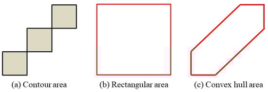
Figure 1.
Contour area, rectangular area, and convex hull area.
In image processing, after extracting the contour surrounding an image object, the area of the image object can be derived by using the spatial moment function as follows:
where and indicate the column and row coordinates of a pixel in the contour set (i.e., boundary pixel set) , respectively. In this research, since it is not necessary to check all the individual pixel values or to consider every coordinate position (that is, it is not necessary to consider the positional influence), the area of a binary image object can be obtained from the moment of the raw spatial moment function. Thus, the area of a binary image extracted from this research corresponds to the sum of the non-zero pixels, i.e., .
4. Experimental Analysis
In this research, four denoising and twelve edge detection techniques are iteratively applied to determine the influence of EMI on the SEM image by extracting the exact image objects and the corresponding various indices. Particularly, after applying these techniques, dilation processing is also adopted to visualize the image object with better clarity. In the denoising step, all four denoising algorithms, i.e., Gaussian filter, median filter, bilateral filter, and non-local mean filter, are applied. The mean squared error (MSE) is used to evaluate the noise reduction effect, and the classification error rate is a user-defined parameter with a range from 0.8 to 0.9. The edge detection parameters are the lower and upper thresholds considered in the Canny edge filter. Figure 2 illustrates the detailed procedures of the proposed method. Here, , , , and indicate the mean squared error of the th denoising technique at the th iteration, the classification accuracy of the th edge detection technique at the th iteration, the threshold value for the mean squared error, and the threshold value for the accuracy, respectively.
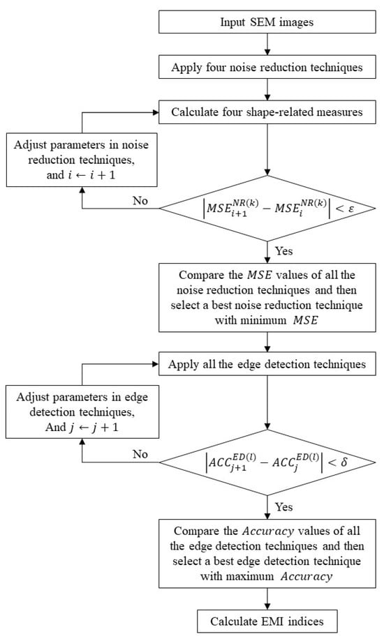
Figure 2.
Flowchart of image object extraction and quantification process.
The experimental results presented in Figure 3 show that the Gaussian filter is selected as the best denoising technique in the first denoising step since it provides the minimum mean squared error compared to other denoising techniques.
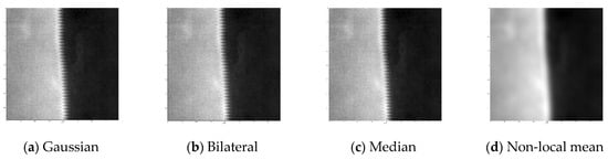
Figure 3.
Results of the 1st denoising.
Then, twelve different edge detection filters are applied to the images refined by the Gaussian filter at the first denoising stage. As shown in Figure 4, the Scharr x filter is selected as the best edge detection technique in the first edge detection process since it provides the maximum classification performance.
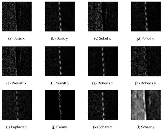
Figure 4.
Results of the 1st edge detection.
As the second denoising method, the Gaussian filter and a non-local mean filter are sequentially applied to the image obtained from the previous step. Then, the Canny edge filter is applied to the image derived from the previous step. Through the iterative application of the denoising and edge detection algorithm selected, it is shown that all edges reflecting the image object deformation are effectively detected. The proposed analysis procedure is tested on 3 different types of 119 semiconductor SEM images, i.e., high-EMI, medium-EMI, and weak-EMI, and 5 distortion measures are extracted from each image, i.e., image object area (denoted by ‘Area’), image object contour (denoted by ‘Perimeter’), rectangular area of the image object (denoted by ‘Rectangular’), extend index (denoted by ‘Extend’), and solidity index (denoted by ‘Solidity’). Here, high-EMI, medium-EMI, and weak-EMI indicate SEM images affected heavily, moderately, and rarely by EMI, respectively. Figure 5 shows the box plots of five measures for three different types of semiconductor SEM images. The x-axis and y-axis in Figure 5 represent three different types of SEM images according to the level of EMI introduced and distortion measures, respectively. As shown in this figure, the medians of all five measures of high-EMI SEM images are higher than those of both medium- and weak-EMI SEM images, and the medians of all five measures of medium-EMI SEM images are higher than those of weak-EMI SEM images.
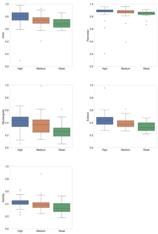
Figure 5.
Comparison of EMI-generated SEM images.
Since the response variable is a categorical (i.e., nominal) variable and independent variables are numeric (i.e., continuous) variables, a multinomial logistic regression is used to model the nominal response variables and predict the probabilities of the different possible responses. The following Table 1 shows the parameter estimation results of multinomial logistic regression analysis of two models, that is, medium-EMI (denoted by ‘Class = 2’) relative to weak-EMI (denoted by ‘Class = 1’) and high-EMI (denoted by ‘Class = 3’) relative to weak-EMI (denoted by ‘Class = 1’), that is, weak-EMI is the base response.

Table 1.
Results of multinomial logistic regression analysis.
Several different types of goodness-of-fit measures have been developed since the conventional cannot be applied to assess goodness of fit in logistic regression analysis. One of the popular goodness-of-fit measures in logistic regression analysis is McFadden’s pseudo--squared statistic based on the ratio of the log-likelihood functions as follows:
where and are the maximum log-likelihood functions for the full model and the intercept-only model (also called the null model), respectively. From the analysis results, it is found that McFadden’s pseudo--squared value of the fitted model is 0.245, and thus, we may conclude that the regression model fits the data moderately well since McFadden’s pseudo--squared value ranges from 0.2 to 0.4, which indicates a very good model fit [45]. And, to test whether all the regression coefficients of predictors in the fitted logistic regression model are simultaneously zero or not (i.e., vs. ), the following log-likelihood ratio (i.e., LLR) statistic can be used:
The LLR -value for testing the fitted full model () versus the intercept-only model () is , and thus, we can conclude that the model fits the data better than the intercept-only model since the LLR -value is less than the significance level of , that is, including all the measures as predictors significantly improves the model fit compared to the intercept-only model. Finally, all the estimates of regression coefficients of both ‘Logit 1’ and ‘Logit 2’ models are statistically significant at the significance level of 0.05. The estimated logistic models of the two classes are
For example, the coefficient of ‘Extend’ is 99.605 in the ‘Logit 1’ model. This indicates that an increase in the ‘Extend’ by one unit will result in an increase of 99.605 units in the log of the ratio between the probability of being a medium EMI versus the probability of being a weak EMI. Finally, to evaluate whether all of these measures are statistically significant in detecting the EMI effect on semiconductor SEM images, a multivariate analysis of variance (MANOVA) is executed, which is useful for testing whether the vectors of means for more than two groups are different or not. Specifically, to compare the difference in the means of all five measures for the type of semiconductor SEM images (i.e., high-EMI, medium-EMI, and weak-EMI image groups), the four most common statistics, i.e., Wilks’ Lambda, Pillai’s trace, Hotelling–Lawely trace, and Roy’s largest root, are considered. The Wilks’ Lambda statistic is as follows:
where and are the determinants of the within-group sum of squares and the between-group sum of squares, respectively. This test statistic ranges from 0 to 1, and the smaller values indicate larger variability between vectors of means. The Pillai’s trace, Hotelling–Lawely trace, and Roy’s largest root statistics are as follows:
The Pillai’s trace value also ranges from 0 to 1, but compared to Wilks’ Lambda, the larger values of the Pillai’s trace, Hotelling–Lawely trace, and Roy’s largest root statistics indicate larger variability between vectors of means [46]. Table 2 shows the result of MANOVA.
Table 2.
Results of multivariate analysis of variance (MANOVA).
For example, Pillai’s trace value is 0.429, and the corresponding F-value is (i.e., p-value < 0.001). Since all the p-values of the test statistics are close to 0, the null hypothesis can be rejected at the significance level of 0.05 where , , and indicate the mean vectors of five measures for three different types of semiconductor SEM images, i.e., high-EMI, medium-EMI, and weak-EMI SEM images, respectively. Therefore, we can conclude that all the extracted shape-related measures are good quantification metrics for assessing the impact of EMI on semiconductor SEM images.
5. Conclusions
Electromagnetic interference (EMI) is one of the crucial problems in semiconductor image analysis. Thus, in this research, four different types of denoising algorithms and twelve different edge detection algorithms are considered to investigate the influence of the EMI on the semiconductor SEM image analysis. From the experimental analysis, it is found that the Gaussian filter for denoising and both the Scharr × filter and the Canny filter for edge detection are the best for characterizing distorted image objects. Additionally, from the statistical analysis, all the measures (i.e., image object area, image object contour, rectangular area of the image object, extend index, and solidity index) are very effective in describing the degree of distortion in semiconductor SEM images caused by EMI since the medians of all the extracted shape-related measures of high-EMI SEM images are higher than those of both medium- and weak-EMI SEM images and all the p-values of the test statistics are close to 0. As for future work, more accurate indices for calibrating the degree of distortion in semiconductor SEM images and the performance of other denoising and edge detection algorithms can be investigated. It is necessary to develop an automatic classification and analysis system for the EMI-generated semiconductor SEM images, including the EMI effect extraction function and yield analysis function.
Author Contributions
Y.-J.P.: conceptualization, investigation, data curation, experiment, writing—original draft, and writing—review and editing. R.P.: conceptualization, methodology, writing—original draft, and writing—review and editing. D.C.M.: conceptualization, methodology, supervision, and writing—review and editing. All authors have read and agreed to the published version of the manuscript.
Funding
This research was funded by the Ministry of Science and Technology of Taiwan, grant number 110-2221-E-027-106-MY3.
Informed Consent Statement
Not applicable.
Data Availability Statement
The data presented in this study are available on request from the corresponding author. The data are not publicly available as it contains confidential information.
Conflicts of Interest
The authors declare no conflicts of interest.
References
- Płuska, M.; Czerwinski, A.; Ratajczak, J.; Kątcki, J.; Oskwarek, Ł.; Rak, R. Separation of image-distortion sources and magnetic-field measurement in scanning electron microscope (SEM). Micron 2009, 40, 46–50. [Google Scholar] [CrossRef] [PubMed]
- Henry, T.; Patterson, O.; Brown, G. Application of ADC techniques to characterize yield-limiting defects identified with the overlay of E-test/inspection data on short loop process testers. In Proceedings of the 10th Annual IEEE/SEMI Advanced Semiconductor Manufacturing Conference and Workshop (ASMC), Boston, MA, USA, 8–10 September 1999; pp. 330–337. [Google Scholar]
- Tobin, K.W.; Lakhani, F.; Karnowski, T.P. An Industry Survey of Automatic Defect Classification Technologies, Methods, and Performance. In Proceedings of the Society of Photo-Optical Instrumentation Engineers (SPIE), Santa Clara, CA, USA, 6–7 March 2002; pp. 46–53. [Google Scholar]
- van Ginneken, B. Fifty years of computer analysis in chest imaging: Rule-based, machine learning, deep learning. Radiol. Phys. Technol. 2017, 10, 23–32. [Google Scholar] [CrossRef] [PubMed]
- Kondo, N.; Harada, M.; Takagi, Y. Efficient Training for Automatic Defect Classification by Image Augmentation. In Proceedings of the 2018 IEEE Winter Conference on Applications of Computer Vision (WACV), Lake Tahoe, CA, USA, 12–15 May 2018; pp. 226–233. [Google Scholar]
- Cheon, S.; Lee, H.; Kim, C.O.; Lee, S.H. Convolutional Neural Network for Wafer Surface Defect Classification and the Detection of Unknown Defect Class. IEEE Trans. Semicond. Manuf. 2019, 32, 163–170. [Google Scholar] [CrossRef]
- O’Leary, J.; Sawlani, K.; Mesbah, A. Deep Learning for Classification of the Chemical Composition of Particle Defects on Semiconductor Wafers. IEEE Trans. Semicond. Manuf. 2020, 33, 72–85. [Google Scholar] [CrossRef]
- Tsai, T.-H.; Lee, Y.-C. A Light-Weight Neural Network for Wafer Map Classification Based on Data Augmentation. IEEE Trans. Semicond. Manuf. 2020, 33, 663–672. [Google Scholar] [CrossRef]
- Yang, Y.-F.; Sun, M. Double feature extraction method for wafer map classification based on convolution neural network. In Proceedings of the 31st Annual SEMI Advanced Semiconductor Manufacturing Conference (ASMC), Saratoga Springs, NY, USA, 24–26 August 2020; pp. 1–6. [Google Scholar]
- Arena, S.; Bodrov, Y.; Carletti, M.; Gentner, N.; Maggipinto, M.; Yang, Y.; Beghi, A.; Kyek, A.; Susto, G.A. Exploiting 2D Coordinates as Bayesian Priors for Deep Learning Defect Classification of SEM Images. IEEE Trans. Semicond. Manuf. 2021, 34, 436–439. [Google Scholar] [CrossRef]
- Tian, P.; Li, C.; Fu, H.; Yu, X.; Wei, Z.; Ni, Q.; Chen, X.; Ding, Y.; Xu, R.; Sun, R. Wafer defect classification based on DCNN model. In Proceedings of the China Semiconductor Technology International Conference (CSTIC), Shanghai, China, 14–15 March 2021; pp. 1–6. [Google Scholar]
- Xu, Y.; Li, D.; Xie, Q.; Wu, Q.; Wang, J. Automatic defect detection and segmentation of tunnel surface using modified Mask R-CNN. Measurement 2021, 178, 109316. [Google Scholar] [CrossRef]
- de la Rosa, F.L.; Sánchez-Reolid, R.; Gómez-Sirvent, J.L.; Morales, R.; Fernández-Caballero, A. A Review on Machine and Deep Learning for Semiconductor Defect Classification in Scanning Electron Microscope Images. Appl. Sci. 2021, 11, 9508. [Google Scholar] [CrossRef]
- de la Rosa, F.L.; Gómez-Sirvent, J.L.; Sánchez-Reolid, R.; Morales, R.; Fernández-Caballero, A. Geometric transformation-based data augmentation on defect classification of segmented images of semiconductor materials using a ResNet50 convolutional neural network. Expert. Syst. Appl. 2022, 206, 117731. [Google Scholar] [CrossRef]
- Gómez-Sirvent, J.L.; de la Rosa, F.L.; Sánchez-Reolid, R.; Morales, R.; Fernández-Caballero, A. Defect classification on semiconductor wafers using Fisher vector and visual vocabularies coding. Measurement 2022, 202, 111872. [Google Scholar]
- Liang, Z.; Tan, G.; Sun, C.; Li, J.; Zhang, L.; Xiong, X.; Liu, Y. An Effective Clustering Algorithm for the Low-Quality Image of Integrated Circuits via High-Frequency Texture Components Extraction. Electronics 2022, 11, 572. [Google Scholar] [CrossRef]
- Nam, Y.; Joo, S.; Kwak, N.; Kim, K.; Kim, D.-N. Precise Pattern Alignment for Die-to-Database Inspection Based on the Generative Adversarial Network. IEEE Trans. Semicond. Manuf. 2022, 35, 532–539. [Google Scholar] [CrossRef]
- Nakagaki, R.; Honda, T.; Nakamae, K. Automatic recognition of defect areas on a semiconductor wafer using multiple scanning electron microscope images. Meas. Sci. Technol. 2009, 20, 075503. [Google Scholar] [CrossRef]
- Płuska, M.; Czerwinski, A.; Ratajczak, J.; Katcki, J.; Rak, R. Elimination of scanning electron microscopy image periodic distortions with digital signal-processing methods. J. Microsc. 2006, 224, 89–92. [Google Scholar] [CrossRef] [PubMed]
- Ning, S.; Fujita, T.; Nie, A.; Wang, Z.; Xu, X.; Chen, J.; Chen, M.; Yao, S.; Zhang, T.-Y. Scanning distortion correction in STEM images. Ultramicroscopy 2018, 184, 274–283. [Google Scholar] [CrossRef] [PubMed]
- Pradelles, J.; Perraud, L.; Fay, A.; Sezestre, E.; Henry, J.-B.; Bustos, J.; Guyez, E.; Berard-Bergery, S.; Le Pennec, A.; Abaidi, M.; et al. Roughness measurement of 2D curvilinear patterns: Challenges and advanced methodology. In Proceedings of the SPIE Advanced Lithography, Online, 22 February 2021; p. 1161110. [Google Scholar]
- Weisbuch, F.; Schatz, J.; Mattick, S.; Schuch, N.; Figueiro, T.; Schiavone, P. Investigating SEM-contour to CD-SEM matching. In Proceedings of the SPIE Advanced Lithography, Online, 9 March 2021; p. 116110Y-2. [Google Scholar]
- Jain, P.; Tyagi, V. A survey of edge-preserving image denoising methods. Inform. Syst. Front. 2016, 18, 159–170. [Google Scholar] [CrossRef]
- Diwakar, M.; Kumar, M. A review on CT image noise and its denoising. Biomed. Signal Process. Control 2018, 42, 73–88. [Google Scholar] [CrossRef]
- Milanfar, P. A Tour of Modern Image Filtering: New Insights and Methods, Both Practical and Theoretical. IEEE Signal Proc. Mag. 2013, 30, 106–128. [Google Scholar] [CrossRef]
- Gonzalez, R.C.; Woods, R.E. Digital Image Processing; Pearson Education: New York, NY, USA, 2018. [Google Scholar]
- Jain, A.K. Fundamentals of Digital Image Processing; Prentice-Hall: Englewood Cliffs, NJ, USA, 1988. [Google Scholar]
- Yang, H.-Y.; Wang, X.-Y.; Qu, T.-X.; Fu, Z.-K. Image denoising using bilateral filter and Gaussian scale mixtures in shiftable complex directional pyramid domain. Comput. Electr. Eng. 2011, 37, 656–668. [Google Scholar] [CrossRef]
- Sun, T.; Neuvo, Y. Detail-preserving median based filters in image processing. Pattern Recogn. Lett. 1994, 15, 341–347. [Google Scholar] [CrossRef]
- Buades, A.; Coll, B.; Morel, J.M. A Review of Image Denoising Algorithms, with a New One. Multiscale Model. Simul. 2005, 4, 490–530. [Google Scholar] [CrossRef]
- Lu, K.; He, N.; Li, L. Nonlocal Means-Based Denoising for Medical Images. Comput. Math. Method. Med. 2012, 2012, 438617. [Google Scholar] [CrossRef] [PubMed]
- Tomasi, C.; Manduchi, R. Bilateral Filtering for Gray and Color Images. In Proceedings of the Sixth International Conference on Computer Vision, Bombay, India, 7 January 1998; pp. 839–846. [Google Scholar]
- Astola, J.; Kuosmanen, P. Fundamentals of Nonlinear Digital Filtering; CRC Press: Boca Raton, FL, USA, 1997. [Google Scholar]
- Pitas, I.; Venetsanopoulos, A.N. Nonlinear Digital Filters: Principles and Applications; Springer: Boston, MA, USA, 1990. [Google Scholar]
- Coupé, P.; Hellier, P.; Kervrann, C.; Barillot, C. Nonlocal Means-Based Speckle Filtering for Ultrasound Images. IEEE T. Image Process. 2009, 18, 2221–2229. [Google Scholar] [CrossRef] [PubMed]
- Frei, W.; Chen, C.-C. Fast Boundary Detection: A Generalization and a New Algorithm. IEEE Trans. Comput. 1977, C-26, 988–998. [Google Scholar] [CrossRef]
- Jing, J.; Liu, S.; Wang, G.; Zhang, W.; Sun, C. Recent advances on image edge detection: A comprehensive review. Neurocomputing 2022, 503, 259–271. [Google Scholar] [CrossRef]
- Kittler, J. On the accuracy of the Sobel edge detector. Image Vis. Comput. 1983, 1, 37–42. [Google Scholar] [CrossRef]
- Zhou, R.-G.; Yu, H.; Cheng, Y.; Li, F.-X. Quantum image edge extraction based on improved Prewitt operator. Quantum Inf. Process. 2019, 18, 261. [Google Scholar] [CrossRef]
- Roberts, L.G. Machine Perception of Three-Dimensional Solids. Ph.D. Thesis, Massachusetts Institute of Technology, Cambridge, MA, USA, 1963. [Google Scholar]
- Canny, J. A Computational Approach to Edge Detection. IEEE Trans. Pattern Anal. Mach. Intell. 1986, 8, 679–698. [Google Scholar] [CrossRef]
- Ding, L.; Goshtasby, A. On the Canny edge detector. Pattern Recogn. 2001, 34, 721–725. [Google Scholar] [CrossRef]
- Pratt, W.K. Digital Image Processing; Wiley-Interscience: New York, NY, USA, 2002. [Google Scholar]
- Scharr, H. Optimal filters for extended optical flow. In Proceedings of the 1st International Conference on Complex Motion (IWCM), Günzburg, Germany, 12–14 October 2004; pp. 14–29. [Google Scholar]
- McFadden, D. Conditional Logit Analysis of Qualitative Choice Behavior. Frontiers in Econometrics; Academic Press: New York, NY, USA, 1973; pp. 105–142. [Google Scholar]
- Johnson, R.A.; Wichern, D.W. Applied Multivariate Statistical Analysis; Prentice-Hall: Englewood Cliffs, NJ, USA, 2007. [Google Scholar]
Disclaimer/Publisher’s Note: The statements, opinions and data contained in all publications are solely those of the individual author(s) and contributor(s) and not of MDPI and/or the editor(s). MDPI and/or the editor(s) disclaim responsibility for any injury to people or property resulting from any ideas, methods, instructions or products referred to in the content. |
© 2023 by the authors. Licensee MDPI, Basel, Switzerland. This article is an open access article distributed under the terms and conditions of the Creative Commons Attribution (CC BY) license (https://creativecommons.org/licenses/by/4.0/).