Abstract
This paper discusses an elliptical ultrawideband (UWB) antenna and a dual-band UWB notch antenna. To achieve a UWB bandwidth, two corner cuts are etched into the rectangular slot on the partial ground plane. An inverted-U-shaped and conductor-shaped resonator are utilized to achieve dual-band notch characteristics on a partial ground plane. The suggested antenna has an overall dimension of . The suggested UWB antenna has a gain of 4.9 dB, a bandwidth of 2.5–11 GHz, a linear phase response, a group delay of less than 1 ns, and a steady radiation pattern. The suggested UWB notch rejects WLAN and ITU bands from 5.2–5.7 GHz and 7.2–8.5 GHz, respectively, with an impedance bandwidth of 2.5–11 GHz. The UWB notch antenna features a linear phase, a group delay of less than 1 ns, and a stable radiation pattern.
1. Introduction
A UWB bandwidth is the frequency band bounded by the points that are 10 dB below the highest radiated emission, as based on the complete transmission system including the antenna. The upper boundary is designated , and the lower boundary is designated . An antenna having a fractional bandwidth equal to or greater than 0.20 or having a UWB bandwidth equal to or greater than 500 MHz, regardless of the fractional bandwidth, is called a UWB antenna. [1,2]. UWB communication, as the name implies, has a large bandwidth and supports a high transmission rate. Ultrawideband antenna applications have recently expanded to cover many computing devices and IoT peripherals [3]. The bulk of these wireless communication systems make use of a UWB antenna for purposes including but not limited to data transfer, reception, localization, location identification, sensing, and tracking.
UWB antenna design varies depending on the communication system’s radiation characteristics, and each application necessitates specialized UWB antennas. Due to developments in impulse technology, low-power communication systems, and the availability of unlicensed frequency bands, UWB has emerged as the dominant technique for short-range wireless communication [4]. Due to its inherent properties, UWB technology is well suited for precisely obtaining spatial and directional data, including a high data rate, a broad bandwidth, a reduction in multipath fading, a low cost, and low power consumption [5].
The recent proliferation of wireless communication, wireless portable devices, and smart consumer electronics has increased demand for ultrawideband antenna applications [6]. UWB antenna design research [7,8,9,10] is undertaken to improve UWB communication systems with new breakthroughs. Moreover, a single UWB antenna may span numerous frequencies, transmission functions, and operation bands. Therefore, their utilization can eliminate the need for many narrowband antennas. The interference caused by several antennas is decreased, and antenna space is conserved. It is crucial to remember that to get the most out of UWB antennas, they must be carefully designed for the individual needs of each system.
Narrowband systems such as WiMAX, WLAN, and C-band, among others, cause significant interference to UWB antennas. Strong disruptions, such as background noise, emerge from these interferences [11]. A notch is built in the UWB antenna to eliminate these intense narrowband interferences. Notch is the technique of removing unwanted frequency bands from the UWB spectrum [12].
In the literature, many UWB notch antennas have been recorded. The authors of article [13] suggest a floret antenna for wideband application. A UWB antenna with an arch-shaped ground plane is proposed using Koch fractal on the hexagonal pattern patch [14]. In paper [15], a UWB antenna with a slot-type split-ring resonator and a defective ground plane is proposed to achieve a dual notch. A dual-band notch antenna using sectorial and inverted U-shaped slots over a rectangular patch is reported in the article [16]. Paper [17] presents a fractal dual-band UWB antenna with a C-shaped complementary split-ring resonator on the patch’s transmission line to perform dual-notch filtering. A dual-notch band UWB antenna is proposed in the article [18] using C-slot and inverted U-slot. A UWB antenna in [19] uses a split-ring slot to create a dual notch. A wide bandwidth in the UWB range is achieved by altering the rectangular patch. In [20], the authors suggest a notch antenna with two bands. A meandering patch slot and a U-shaped feed slot provide a 3–3.9 and 5.22–5.7 GHz notch band. In [21], the patch’s two U-shaped stubs create a 3.0–3.9 GHz and 5.0–5.9 GHz notch band.
In this article, an elliptical UWB notch antenna has been designed and fabricated to cover UWB channel 1 to 15, i.e., low band (UWB channels 1 to 4) and high band (UWB channels 5 to 15). The addition of parasitic resonators for UWB notch antenna overcomes electromagnetic interference between bands by inserting inverted-U-shaped and iron-shaped parasitic resonators on the ground plane. Evolution steps from the UWB antenna to the UWB notch antenna are discussed. Section 2 and Section 3 discuss the technique for designing antennas. Section 4 discusses result analysis. Section 5 discusses the conclusion followed by references.
2. UWB Antenna Design Approach
The evolution of the UWB antenna is depicted in Figure 1, while the S11 characteristics are depicted in Figure 2. In the first stage, an ellipse radiating patch and a rectangle ground plane are created. However, the S11 value is much higher than −10 dB.
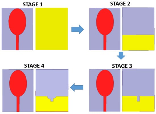
Figure 1.
Progression stage of UWB antenna.
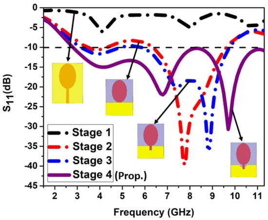
Figure 2.
S11 characteristics of UWB antenna.
As a result, the ground plane was further modified in stage 2 to become a partly rectangular ground plane. The S11 value decreases as a result. In stage 3, a partially rectangular ground plane is slotted to improve S11. The rectangular slot on the ground plane significantly brings the S11 value below −10 dB, but it does not cover the UWB range. As a result, in stage 4 of Figure 1, more modifications are made to obtain UWB characteristics in the antenna. Two corner cuts are etched on the rectangular slot on the ground plane. It gives the impedance bandwidth from 2.5–11 GHz, which covers the UWB range.
3. UWB Notch Antenna Design Approach
Figure 3 shows the design of an elliptical UWB notch antenna. After completing the design of the elliptical-shaped UWB antenna, the notches have to be introduced. There are many techniques to obtain notches. Two parasitic resonators, an inverted-U-shaped resonator and an iron-shaped resonator, are used to achieve the notch. The inverted-U-shaped resonator helps obtain a notch at 5.3 GHz, and the iron-shaped resonator helps in obtaining a notch at 8.1 GHz. Figure 4 shows the dimension of the suggested antenna. Table 1 lists the antenna’s dimensions.
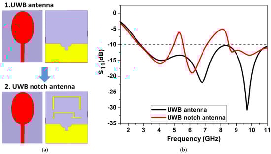
Figure 3.
Elliptical UWB notch antenna: (a) UWB to UWB notch; (b) S11.
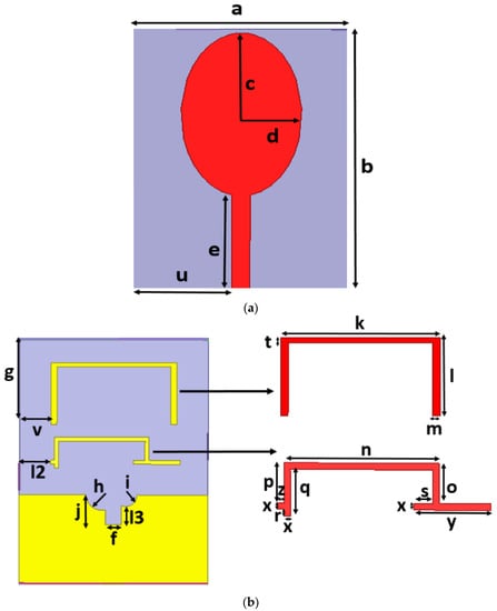
Figure 4.
Dimension of elliptical UWB notch antenna: (a) patch; (b) ground plane.

Table 1.
Dimension of the proposed antenna.
The length of truncation in the ground plane for achieving UWB is calculated using Equation (1).
The relative permittivity of the FR-4 substrate is , so effective permittivity can be calculated as Equation (2),
As we can observe that the first notch frequency, , and is due to the effect of the upper resonator. Therefore, mathematically, the length of the upper resonator can be calculated using Equation (3).
Similarly, the second notch frequency, and is due to the effect of the lower resonator. Therefore, mathematically, the length of the lower resonator can be calculated using Equation (4).
3.1. Progression of UWB Notch Antenna
This section describes the evolution stages of a UWB notch antenna. It shows a step-by-step iterative process to arrive at the final structure. The following Figure 5 shows a pictorial representation of the iterative process.
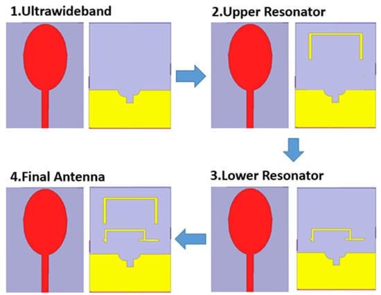
Figure 5.
Progression stage of UWB notch antenna.
A patch and a ground plane make up the proposed antenna. Both of these have undergone modification to arrive at the final structure. The S11 characteristics of the UWB notch antenna at every stage are plotted together and depicted in Figure 6.
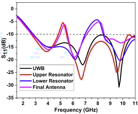
Figure 6.
S11 characteristics of progression stage of UWB notch antenna.
In step 1, the UWB antenna is designed. The ground plane is then etched with an in-verted-U-shaped upper resonator in step 2. The inverted-U-shaped upper resonator gives the first notch at 5.3 GHz, as shown in Figure 5. In step 3, an iron-shaped lower resonator is added to the ground plane. The iron-shaped lower resonator gives the second notch at 8.1 GHz. Thus, the upper resonator and lower resonator combination make an elliptical UWB notch antenna in step 4.
These graphs in Figure 6 show that the notch antenna has S11 < −10 dB for the entire UWB range and has two notches at 5.3 GHz and 8.1 GHz due to the two resonators.
3.2. Parametric Analysis of UWB Notch Antenna
The impact of the stubs dimension on the notch antenna is examined using a parametric analysis. The dimensions t and x have an impact on the design’s performance.
3.2.1. Effect of Upper Resonator-Width ‘t’
To analyze the effects of width ‘t’ on the S11 characteristics, the variation in width ‘t’ was simulated and analyzed. The S11 characteristics are represented in Figure 7. When the width is 0.5 mm, the result is optimum.
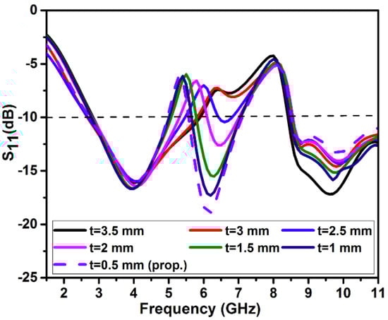
Figure 7.
S11 for variation of width ‘t’.
3.2.2. Effect of Lower Resonator-Width ‘x’
The variation in width ‘x’ is simulated and studied to investigate the effects of width ‘x’ on the S11 features. Figure 8 illustrates the S11 features. The result is best when the width is 0.5 mm.
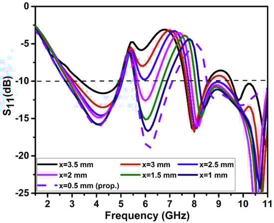
Figure 8.
S11 for variation of width ‘x’.
4. Discussion and Outcomes
The suggested antenna is subjected to a full-wave simulation using HFSS. ROHDE & SCHWARZ ZVL 13 network analyzer is used to conduct measurements.
4.1. UWB Antenna Results
The intended ultrawideband (UWB) antenna, shown in Figure 9, was fabricated according to the design.
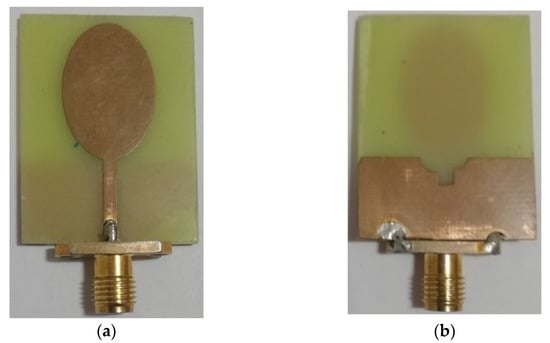
Figure 9.
Suggested UWB antenna: (a) patch; (b) ground plane.
4.1.1. VSWR
Figure 10 compares simulated and measured VSWR. ROHDE & SCHWARZ ZVL network analyzer measures VSWR. At VSWR < 2, the simulated impedance bandwidth is 2.8–11.2 GHz, and the operational impedance bandwidth is 2.5–11 GHz. Simulations and measurements of VSWR exhibit a minor difference. This is due to the effect of soldering, the failure to account for the SMA connector during simulation, flaws in the dielectric constant of the substrate, and manufacturing tolerances.
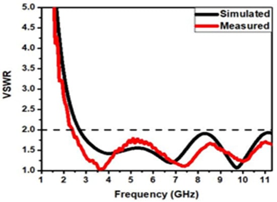
Figure 10.
VSWR, simulated and measured.
4.1.2. Current Distribution
Figure 11 illustrates a simulation and study of the current distribution to illustrate the functionality of the proposed UWB antenna. At 3.6, 6.8, and 9.7 GHz, the resonance qualities are examined. Figure 11 shows how different antenna parts have varied resonance patterns for different operating modes. In Figure 11a, the lower portion of the feed is active at 3.6 GHz, where the current is highest. In Figure 11b, the feed at 6.8 GHz has the highest current. Figure 11c reveals that the lower portion of the patch and feed are most active at 9.7 GHz. Thus, the antenna resonates at 3.6, 6.8, and 9.7 GHz.
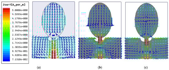
Figure 11.
Current distribution at (a) 3.6 GHz, (b) 6.8 GHz, (c) 9.7 GHz.
4.1.3. Radiation Pattern
Figure 12 depicts the simulation of the antenna radiation pattern for resonant frequencies within the operating band. At 3.6 GHz, a bidirectional pattern is detected in the E-plane, while an omnidirectional pattern is observed in the H-plane. However, at higher frequencies (i.e., 9.7 and 12.6 GHz) the pattern is disturbed due to higher harmonics; in addition, the cross-polarization radiation magnitudes dominate the pattern. It is evident from the figure that the cross-polarization value is much lower than the co-polarization value.
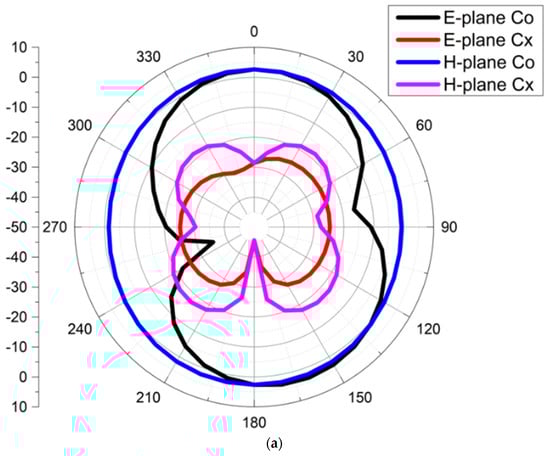
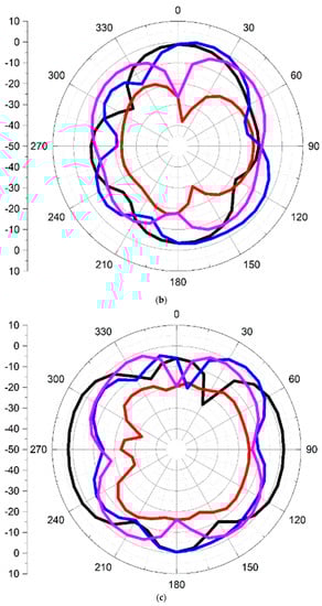
Figure 12.
The simulated radiation pattern of the UWB antenna at (a) 3.6 GHz, (b) 6.8 GHz, and (c) 9.7 GHz.
4.1.4. Time-Domain Characteristics
The phase response, group delay, and isolation properties of the proposed UWB antenna can only be determined by a time-domain analysis. As can be seen in Figure 13, two identical antennas were placed in HFSS 100 mm apart for these tests. The time-domain study considered both forward- and side-facing scenarios.
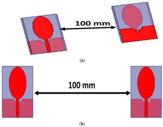
Figure 13.
Time-domain analysis with orientations, viz., (a) frontal and (b) lateral.
In Equation (5), GD is the derivative of phase response to angular frequency.
The proposed UWB antenna’s group delay is depicted in Figure 14. As can be seen in Figure 14, the group delay of the antenna remains relatively the same, regardless of whether it is operating in a face-to-face or side-to-side configuration.
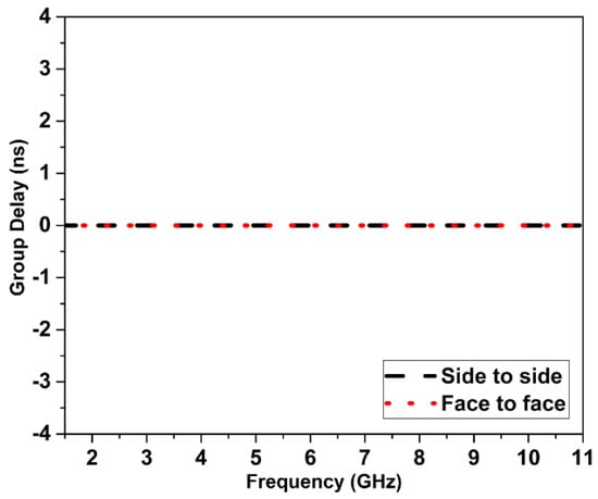
Figure 14.
Group delay proposed UWB antenna.
Figure 15 shows the antenna’s phase response. Linear phase variation yields desirable time-domain features. Figure 15 demonstrates that the phase fluctuation of the antenna is nearly linear during face-to-face and side-to-side operations.
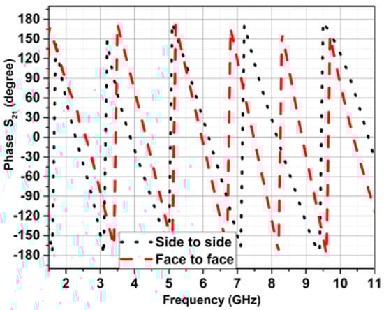
Figure 15.
Phase response S21 of the proposed UWB design.
Isolation features of the proposed UWB antenna are depicted in Figure 16. Figure 16 shows that the antenna has good isolation characteristics (S21 < −20 dB).
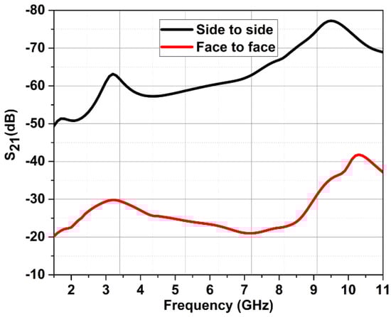
Figure 16.
Isolation characteristics of the UWB antenna.
When computing the fidelity factor, a frontal orientation, as well as a lateral orientation, are both used. Both the input signals and output signals are normalized, as shown in Figure 17. The FF is computed using the normalized transmitted and received pulses in accordance with Equations (6)–(8) [22].
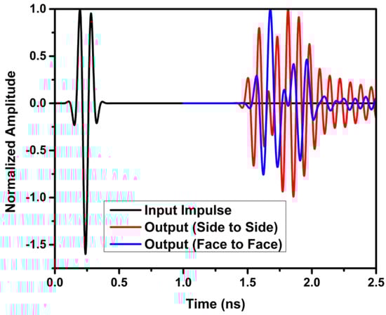
Figure 17.
Fidelity factor.
Normalization is performed to ensure that only the signal’s structure and not its amplitude is evaluated. The estimated fidelity factor values ensure that interference has a negligible effect on the received pulse at the receiver. The fidelity factor in frontal and lateral configurations is more than 98%. The greater value of the fidelity factor assures that the transmitted and received pulses are identical.
4.1.5. Gain
Figure 18 depicts a 3D gain plot at resonant frequencies at 3.6 GHz, 6.8 GHz, and 9.7 GHz. At 3.6 GHz, 6.8 GHz, and 9.7 GHz, the gain is 2.38 dB, 3.44 dB, and 4.85 dB.
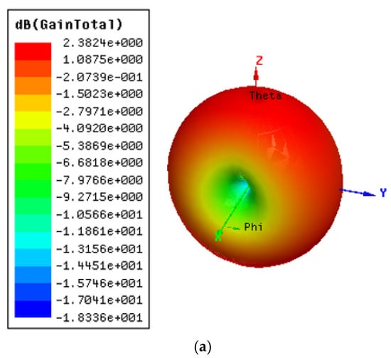
Figure 18.
D gain plot at (a) 3.6 GHz, (b) 6.8 GHz, and (c) 9.7 GHz.
Figure 19 shows that a maximum gain of 4.9 dB is achieved for the UWB microstrip antenna.
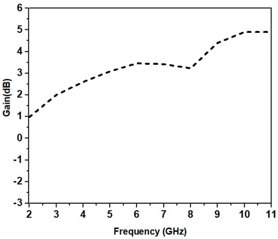
Figure 19.
Gain of UWB antenna.
4.2. Outcome of Ultrawideband Notch Antenna
The intended ultrawideband notch antenna, shown in Figure 20, was fabricated according to the design.
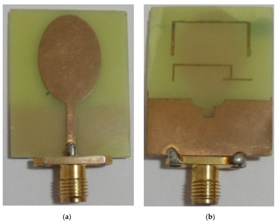
Figure 20.
Fabricated proposed UWB notch antenna: (a) patch; (b) ground.
4.2.1. VSWR
Figure 21 shows a comparison of the UWB notch antenna’s simulated and measured VSWR. Strong rejection can be seen in the simulated VSWR plot between the WLAN band of 5–5.6 GHz and the ITU band of 7.1–8.5 GHz, with a fractional bandwidth of almost 120% (2.8–11.2 GHz). The measured VSWR plot demonstrates a high level of attenuation across the WLAN band (5.2–5.7 GHz) and the ITU band (7.2–8.5 GHz), with a fractional bandwidth of around 125%. (2.5–11 GHz). The difference in VSWR between simulated and measured values should be attributed mostly to the influence of SMA connector soldering and fabrication tolerance.
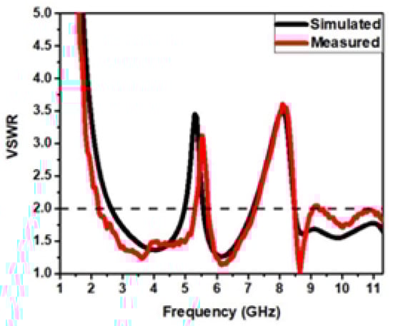
Figure 21.
VSWR of UWB notch antenna, simulated and measured.
4.2.2. Current Distribution
Figure 22 depicts the surface current distributions at notched frequencies of 5.3 GHz and 8.1 GHz with parasitic resonators, illustrating the role of parasitic inverted-U-shaped and iron-shaped resonators in achieving the notched bands. At notched frequencies, surface currents on the elliptical patch flow opposite to the surface current on the ground plane, which contains parasitic elements. Accordingly, the radiation has little to no effect at the notch frequencies. It makes two notches at around 5.3 GHz and 8.1 GHz.
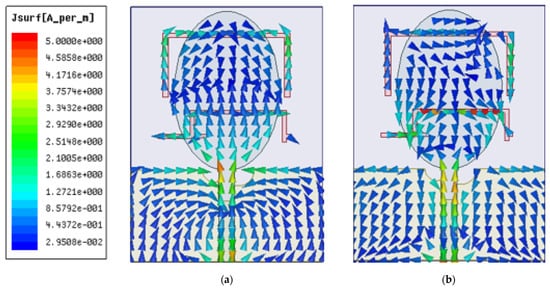
Figure 22.
Current distribution at (a) 5.3 GHz and (b) 8.1 GHz.
4.2.3. Radiation Pattern
Figure 23 depicts the simulation of the antenna radiation pattern for resonant notch frequencies within the operating band.
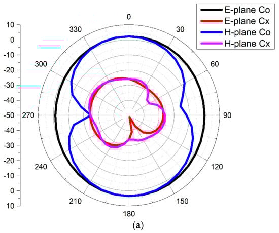
Figure 23.
The simulated radiation pattern at (a) 4 GHz, (b) 6.2 GHz, and (c) 11.7 GHz.
At 4 GHz and 6.2 GHz, an omnidirectional pattern is detected in the E-plane, while a bidirectional pattern is observed in the H-plane. At 11.7 GHz, an omnidirectional pattern is seen in the E-plane and the H-plane.
4.2.4. Time-Domain Characteristics
Figure 24 illustrates analysis in the time domain, which includes group delay, isolation characteristics, and the fidelity factor for the proposed antenna. As mentioned in Section 4.1.4, these studies are carried out similarly.
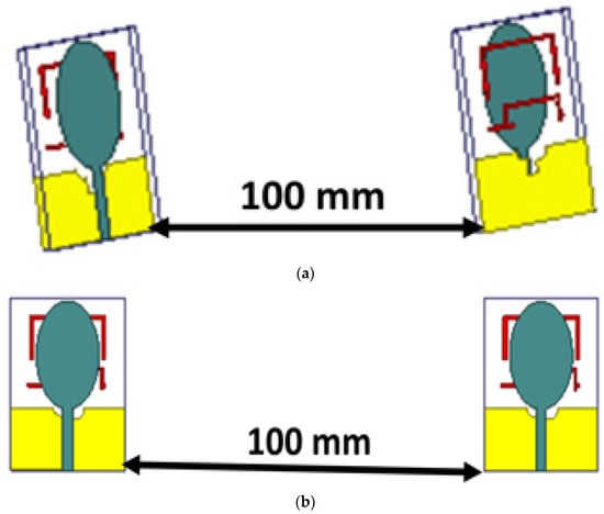
Figure 24.
Time-domain analysis with orientations, viz., (a) frontal and (b) lateral.
Figure 25 shows a high delay at both notched frequencies (5.3 and 8.1 GHz), but the group delay for the face-to-face and side-to-side configurations is less than 1 ns at all other frequencies.
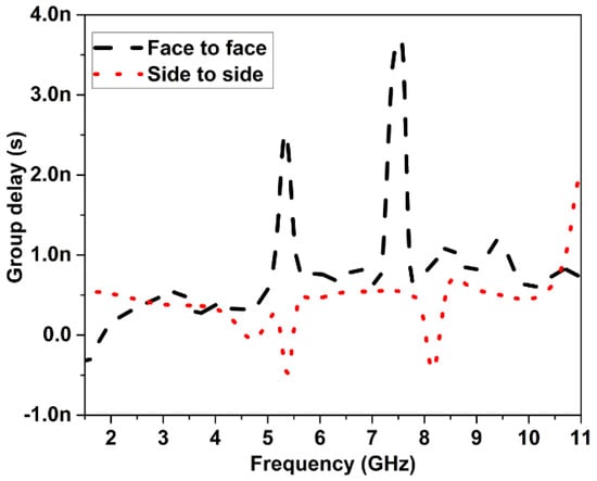
Figure 25.
Group delay of proposed UWB notch antenna.
Figure 26 exhibits the phase variation of the input impedance of the proposed UWB notch antenna. The phase fluctuation throughout the operating band is linear, with the exception of the notched band’s center frequencies, which are around 5.3 and 8.1 GHz. This difference in phase versus frequency in the notched band verifies that the signal’s frequency components have a delay at the notched frequencies.
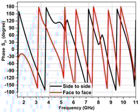
Figure 26.
Phase response S21 of the proposed UWB notch antenna.
Figure 27 shows that the antenna has good isolation characteristics (S21 < −20 dB). The fidelity factor in frontal and lateral configurations is more than 99%, as shown in Figure 28. The greater value of the fidelity factor ensures that the transmitted and received pulses are identical.
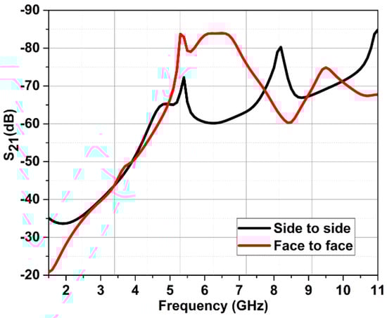
Figure 27.
Isolation characteristics.
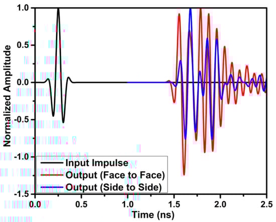
Figure 28.
Fidelity factor of the UWB notch antenna.
For dual-band-notched UWB applications, the time domain analysis of antenna parameters shows that the suggested antenna is a good contender.
4.2.5. Gain of UWB Notch Antenna
Figure 29 shows the total gain of the UWB notch antenna. A maximum gain of 5.9 dB is achieved for the UWB notch antenna.
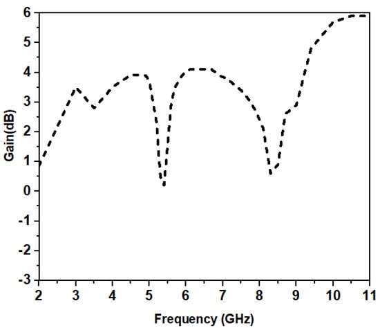
Figure 29.
Gain of the UWB notch antenna.
4.2.6. Comparison Table
The expected design performance is assessed by comparing it to previously published UWB notch antenna designs, as shown in Table 2.
Table 2.
Comparison of the proposed antenna with previous works.
5. Conclusions
An elliptical ultrawideband (UWB) antenna and a dual-band UWB notch antenna are described in this study. The rectangular slot on the partial ground plane is carved with two corner cuts in order to obtain UWB bandwidth. On a partial ground plane, two parasitic resonators, one of which is an inverted-U-shaped resonator, and the other of which is an iron-shaped resonator, are employed in order to obtain dual-band notch characteristics. The suggested antenna has an overall size of . The suggested UWB antenna has a gain of 4.9 dB, an impedance bandwidth of 2.5–11 GHz, a linear phase response, a group delay of less than one nanoseconds, and a consistent radiation pattern. The proposed UWB notch antenna demonstrates high rejection in the WLAN band between 5.2 and 5.7 GHz, with a sharp notch at 5.3 GHz, and in the ITU band between 7.2 and 8.5 GHz, with a sharp notch at 8.1 GHz, with an impedance bandwidth ranging from 2.5 to 11 GHz. The UWB notch antenna has a linear phase, less than 1 ns group delay, and a steady radiation pattern.
Author Contributions
Conceptualization, O.P.K., T.A., P.K. (Pramod Kumar), P.K. (Pradeep Kumar) and J.A.; Methodology, O.P.K., T.A., P.K. (Pradeep Kumar) and J.A.; Software, O.P.K.; Validation, O.P.K. and T.A.; Formal analysis, O.P.K. and P.K.; Investigation, O.P.K., T.A. and P.K. (Pramod Kumar); Resources, P.K. (Pramod Kumar), P.K. (Pradeep Kumar) and J.A.; Data curation, O.P.K.; Writing—original draft, O.P.K.; Writing—review & editing, T.A., P.K. (Pramod Kumar), P.K. (Pradeep Kumar) and J.A.; Visualization, T.A. and J. Supervision, T.A., P.K. (Pramod Kumar) and J.A.; Project administration, T.A. All authors have read and agreed to the published version of the manuscript.
Funding
This research received no external funding.
Institutional Review Board Statement
Not applicable.
Informed Consent Statement
Not applicable.
Data Availability Statement
Not applicable.
Conflicts of Interest
The authors declare no conflict of interest.
References
- Federal Communications Commission. First Report and Order on Ultra-Wideband Technology; FCC 02-48; Federal Communications Commission: Washington, DC, USA, 2002. [Google Scholar]
- Kumar, O.P.; Kumar, P.; Ali, T.; Kumar, P.; Vincent, S. Ultrawideband Antennas: Growth and Evolution. Micromachines 2021, 13, 60. [Google Scholar] [CrossRef] [PubMed]
- NXP. NXP Secure UWB Deployed in Samsung Galaxy Note 20 Ultra Bringing the First UWB-Enabled Android Device to Market. Available online: https://www.nxp.com/company/about-nxp/nxp-secure-uwb-deployed-in-samsung-galaxy-note20-ultra-bringing-the-first-uwb-enabled-android-device-to-market:NW-SECURE-UWB-SAMSUNG-GALAXY (accessed on 11 August 2020).
- Kumar, O.P.; Kumar, P.; Ali, T. A Compact Dual-Band Notched UWB Antenna for Wireless Applications. Micromachines 2021, 13, 12. [Google Scholar] [CrossRef] [PubMed]
- Cadence. Ultra-Wideband Antenna Applications in Communication Systems. In Cadence System Analysis; 2021; Available online: https://resources.system-analysis.cadence.com/blog/msa2021-ultra-wideband-antenna-applications-in-communication-systems (accessed on 11 August 2020).
- Kumar, P.; Pai, M.M.; Ali, T. Ultrawideband antenna in wireless communication: A review and current state of the art. Telecommun. Radio Eng. 2020, 79, 929–942. [Google Scholar] [CrossRef]
- Kumar, P.; Pathan, S.; Vincent, S.; Kumar, O.P.; Yashwanth, N.; Kumar, P.; Shetty, P.; Ali, T. A Compact Quad-Port UWB MIMO Antenna with Improved Isolation Using a Novel Mesh-Like Decoupling Structure and Unique DGS. IEEE Trans. Circuits Syst. II Express Briefs 2022. [Google Scholar] [CrossRef]
- Kumar, P.; Ali, T.; Kumar, O.P.; Vincent, S.; Kumar, P.; Nanjappa, Y.; Pathan, S. An Ultra-Compact 28 GHz Arc-Shaped Millimeter-Wave Antenna for 5G Application. Micromachines 2023, 14, 5. [Google Scholar] [CrossRef] [PubMed]
- Kumar, O.P.; Kumar, P.; Ali, T. A Novel Arc-shaped UWB Antenna for Wireless Applications. In Proceedings of the 6th International Conference on Green Technology and Sustainable Development(GTSD), Nha Trang City, Vietnam, 29–30 July 2022; IEEE: Piscataway, NJ, USA, 2022. [Google Scholar]
- Kumar, O.P.; Kumar, P.; Ali, T. A Novel Ultrawideband Antenna with Band Notching Facilities at WLAN, C-band, and X-band. In Proceedings of the IEEE 19th India Council International Conference (INDICON), Kochi, India, 24–26 November 2022; IEEE: Piscataway, NJ, USA, 2022. [Google Scholar]
- Mahfuz, M.H.; Islam, M.R.; Habaebi, M.H.; Sakib, N.; Hossain, A.Z. A notched UWB microstrip patch antenna for 5G lower and FSS bands. Microw. Opt. Technol. Lett. 2022, 64, 796–802. [Google Scholar] [CrossRef]
- Agarwal, N.; Nidadadvolu, A.; Vincent, S.; Kumar, O.P.; Ali, T. A triple band rectangular shaped patch antenna for GNSS/WiMAX applications. AIP Conf. Proc. 2020, 2297, 020012. [Google Scholar]
- Bharadwaj, A.; Vincent, S.; Ali, T. The Floret Antenna for Terahertz Applications. Optik 2023, 272, 170335. [Google Scholar] [CrossRef]
- Gorai, A.; Pal, M.; Ghatak, R. A Compact fractal-shaped antenna for ultrawideband and bluetooth wireless systems with WLAN rejection functionality. IEEE Antennas Wirel. Propag. Lett. 2017, 16, 2163–2166. [Google Scholar] [CrossRef]
- Lakrit, S.; Das, S.; El Alami, A.; Barad, D.; Mohapatra, S. A compact UWB monopole patch antenna with reconfigurable Band-notched characteristics for Wi-MAX and WLAN applications. AEU-Int. J. Electron. Commun. 2019, 105, 106–115. [Google Scholar] [CrossRef]
- Garg, R.K.; Nair, M.V.D.; Singhal, S.; Tomar, R. A miniaturized ultra-wideband antenna using “modified” rectangular patch with rejection in WiMAX and WLAN bands. Microw. Opt. Technol. Lett. 2021, 63, 1271–1277. [Google Scholar] [CrossRef]
- Hosain, M.M.; Kumari, S.; Tiwary, A.K. Sunflower shaped fractal filtenna for WLAN and ARN application. Microw. Opt. Technol. Lett. 2020, 62, 346–354. [Google Scholar] [CrossRef]
- Nan, J.; Zhao, J.Y.; Wang, Y. A Compact Dual Notch-Band Frequency Reconfigurable UWB Monopole Antenna. Prog. Electromagn. Res. M 2021, 106, 215–226. [Google Scholar] [CrossRef]
- Kaur, K.; Kumar, A.; Sharma, N. Split Ring Slot Loaded Compact CPW-Fed Printed Monopole Antennas for Ultra-Wideband Applications with Band Notch Characteristics. Prog. Electromagn. Res. C 2021, 110, 39–54. [Google Scholar] [CrossRef]
- Sohail, A.; Alimgeer, K.S.; Iftikhar, A.; Ijaz, B.; Kim, K.W.; Mohyuddin, W. Dual notch band UWB antenna with improved notch characteristics. Microw. Opt. Technol. Lett. 2018, 60, 925–930. [Google Scholar] [CrossRef]
- Pratap Singh, A.; Khanna, R.; Singh, H. UWB antenna with dual notched band for WiMAX and WLAN applications. Microw. Opt. Technol. Lett. 2017, 59, 792–797. [Google Scholar] [CrossRef]
- Kumar, P.; Pathan, S.; Kumar, O.P.; Vincent, S.; Nanjappa, Y.; Kumar, P.; Ali, T. Design of a Six-Port Compact UWB MIMO Antenna with a Distinctive DGS for Improved Isolation. IEEE Access 2022, 10, 112964–112974. [Google Scholar] [CrossRef]
- Yang, B.; Qu, S. A compact integrated Bluetooth UWB dual-band notch antenna for automotive communications. AEU-Int. J. Electron. Commun. 2017, 80, 104–113. [Google Scholar] [CrossRef]
- Jaglan, N.; Kanaujia, B.K.; Gupta, S.D.; Srivastava, S. Design of band-notched antenna with DG-CEBG. Int. J. Electron. 2018, 105, 58–72. [Google Scholar] [CrossRef]
- Chilukuri, S.; Gogikar, S. A CPW fed denim based wearable antenna with dual band-notched characteristics for UWB applications. Prog. Electromagn. Res. C 2019, 94, 233–245. [Google Scholar] [CrossRef]
- Puri, S.C.; Das, S.; Gopal Tiary, M. An UWB trapezoidal rings fractal monopole antenna with dual-notch characteristics. Int. J. RF Microw. Comput.-Aided Eng. 2019, 29, e21777. [Google Scholar] [CrossRef]
- Fertas, K.; Ghanem, F.; Azrar, A.; Aksas, R. UWB antenna with sweeping dual notch based on metamaterial SRR fictive rotation. Microw. Opt. Technol. Lett. 2020, 62, 956–963. [Google Scholar] [CrossRef]
- Puri, S.C.; Das, S.; Tiary, M.G. UWB monopole antenna with dual-band-notched characteristics. Microw. Opt. Technol. Lett. 2020, 62, 1222–1229. [Google Scholar] [CrossRef]
- Sharma, N.; Bhatia, S.S. Design of printed monopole antenna with band notch characteristics for ultra-wideband applications. Int. J. RF Microw. Comput.-Aided Eng. 2019, 29, e21894. [Google Scholar] [CrossRef]
- Li, J.; Sun, Y. Design of reconfigurable monopole antenna with switchable dual band-notches for UWB applications. Prog. Electromagn. Res. C 2019, 96, 97–107. [Google Scholar] [CrossRef]
- Zhang, J.; Chen, T.; Lv, Y.; Xing, H. A practical CPW-fed UWB antenna with reconfigurable dual band-notched characteristics. Prog. Electromagn. Res. M 2019, 81, 117–126. [Google Scholar] [CrossRef]


Disclaimer/Publisher’s Note: The statements, opinions and data contained in all publications are solely those of the individual author(s) and contributor(s) and not of MDPI and/or the editor(s). MDPI and/or the editor(s) disclaim responsibility for any injury to people or property resulting from any ideas, methods, instructions or products referred to in the content. |
© 2023 by the authors. Licensee MDPI, Basel, Switzerland. This article is an open access article distributed under the terms and conditions of the Creative Commons Attribution (CC BY) license (https://creativecommons.org/licenses/by/4.0/).