Abstract
Accurate modeling of threshold voltage is necessary in the integrated circuit design of strained silicon devices. Thoroughly researching the factors that affect threshold voltage and establishing a more precise threshold voltage model, can provide essential theoretical support for integrated circuit design. By solving a Poisson equation, in this paper, we demonstrate a comprehensive physical model for the threshold voltage of strained Si NMOSFETs using the gradual channel approximation theory and a quasi-two-dimensional analysis. The model investigates the physical effects such as short-channel, narrow-channel, non-uniform doping, and drain-induced barrier lowering effects on the threshold voltage. After substituting the extracted parameters into the model, a comparison was made with experimental results to validate the accuracy and correctness of the established model. Additionally, variations in the tunneling current of small-sized devices were studied. The two models provide essential references for the analysis and design of strained Si large-scale integrated circuits.
1. Introduction
Strained Si materials offer the advantages of high carrier mobility, adjustable band gap, and compatibility with the traditional Si process. They are the preferred alternative in research on high-speed, high-performance, scaled MOSFETs [1,2]. Threshold voltage is the most critical parameter of MOSFETs, and it affects the AC/DC and subthreshold characteristics of the device. Research on the threshold voltage of strained silicon devices is significant, as it determines the devices’ on-off characteristics. Studying the threshold voltage of strained silicon devices helps to understand their operating state and features and can lead to optimized device design and improved performance and reliability. As device dimensions continue to shrink, the influence of short-channel effect becomes more significant. Strained silicon devices can mitigate or suppress short-channel effect through strain engineering techniques, and the threshold voltage is a crucial parameter in studying these effects. Accurate control of the threshold voltage and accurate threshold voltage adjustment are crucial for process optimization and device fabrication. Researching the threshold voltage of strained silicon devices can facilitate the development of improved process methods and technologies, enabling more precise and stable control of threshold voltage, thereby enhancing process controllability and stability. When designing integrated circuits using strained silicon devices, it is necessary to have an accurate threshold voltage model. By delving into the factors that influence threshold voltage, more precise models can provide essential theoretical support for integrated circuit design and for optimizing performance to meet design requirements. So, research on the threshold voltage of strained silicon devices plays a significant role in optimizing device performance, suppressing short-channel effect, optimizing processes, and supporting integrated circuit design. In current state-of-the-art chip designs, to stop short-channel effect, advanced device designs are extensively used, and strained silicon devices are among these designs. Examples include Intel’s Core processor using 32 nm process technology and TSMC’s 7 nm process, where strained silicon technology has been implemented. This research is essential for advancing the development and application of strained silicon technology. There are many studies on the threshold voltage of strained Si NMOSFETs [3,4,5,6,7]. However, the influences of substrate bias, short-channel effect, narrow-channel effect, and drain-induced barrier lowering effect on threshold voltage have still not been fully considered, and therefore the results cannot be fully applied to the design requirements of devices and integrated circuits under realistic process conditions.
In this paper, a threshold voltage model of a long channel is built using the gradual channel approximation theory and the potential of the strain Si MOSFET longitudinal is analyzed. The influence of substrate bias on threshold voltage is fully considered in the model. However, a one-dimension method cannot meet the requirement of threshold voltage accuracy for scaled devices. To improve the threshold voltage accuracy, two-dimensional and quasi-two-dimensional analysis methods are often used [8,9]. When solving a two-dimensional Poisson equation in the depletion region utilizing a two-dimensional method, the physical meaning of model parameters is deficient due to some approximations made on boundary conditions. In this paper, a quasi-two-dimensional method is used to solve a two-dimensional Poisson equation. A threshold voltage model is built fully considering the short-channel effect, DIBL effect, and the narrow-channel effect. To ensure that the simulation results can better match test results, it is necessary to correct the model using process parameters [10]. So, an integrated physical compact model for threshold voltage of a strained Si NMOSFET is built fully considering the physical effects on threshold voltage.
Through experiments, devices of different sizes were fabricated under the same process conditions, and relevant parameters were extracted using parameter extraction software. The calculation results of the model were compared with the simulation results, which further proved the correctness of the threshold voltage intensive physical model of strained Si NMOSFETs established in this paper. The results provide an important reference for the analysis and design of strained Si devices and also provide an essential theoretical basis for further integrated circuit design.
Tunneling current is a crucial parameter in strained silicon devices, as it reflects the electron tunneling through the bandgap or energy barrier in the strained silicon structure. By studying tunneling current, the performance of a device under low-voltage conditions, including conduction capability, energy efficiency, and noise characteristics, can be evaluated. As device dimensions continue to shrink, tunneling current becomes more significant in strained silicon devices. Therefore, research on tunneling current is significant for limiting device size and achieving micro- and nanoscale devices. By understanding and controlling tunneling current, design and process optimization can be conducted to reduce the increase in tunneling current caused by size effects. Tunneling current is also a key factor that affects the reliability of strained silicon devices. Understanding the sources, characteristics, and mechanisms of tunneling current helps to find methods to reduce or suppress tunneling current, thus improving device reliability and reducing the probability of failure. Research on tunneling current in strained silicon devices provides a foundation for developing new technologies and applications. Understanding the characteristics and control methods of tunneling current can provide critical guidance and support for designing novel devices and developing new strained silicon technologies. In conclusion, studying tunneling current in strained silicon devices is important for evaluating performance, limiting device size, enhancing reliability, and advancing strained silicon technology. This research has a significant impact and guiding value in optimizing device design, improving processes, and promoting the application of strained silicon technology in the field of microelectronics.
2. Theoretical Model Derivation
Biaxial strain can significantly increase electron mobility and is widely used in strained Si NMOSFETs [11,12]. Figure 1 shows the sectional structure of a strained Si NMOSFET. A graded layer with a Ge composition gradient is grown on the Si substrate, which can effectively reduce surface scattering and increase electron mobility. A thick relaxed layer is grown on the graded layer, serving as a virtual substrate. Finally, a very thin Si layer is epitaxially grown on the relaxed layer, introducing tensile strain in the Si layer due to different lattice constants between the Si and layers. S, G, D, and B represent the source, gate, drain, and substrate contacts, respectively. and are the thicknesses of the strained Si layer and substrate depletion layer, respectively. and are the doping concentrations of the strained Si layer and relaxed layer, respectively.
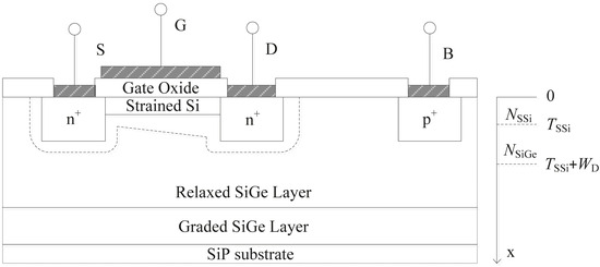
Figure 1.
Cross-sectional structure of a strained Si NMOSFET.
2.1. Long-Channel Threshold Voltage Model
Strictly speaking, modeling a MOSFET is a three-dimensional problem. However, from a practical standpoint (unless the channel width W and channel length L are tiny), it can be approximated as a two-dimensional system, which means considering only the y-direction along the channel and the x-direction perpendicular to the channel. Additionally, if the variation in the electric field Ey along the y-direction is much smaller than that in the corresponding electric field Ex along the x-direction, the device can be treated using a one-dimensional approximation method.
2.1.1. Zero Substrate Bias Threshold Voltage Model ()
The device structure shown in Figure 1 establishes and solves a one-dimensional Poisson’s equation along the x-direction, perpendicular to the channel, when the substrate bias is zero, i.e., . Therefore, the threshold voltage model for strained Si NMOSFETs can be derived with long channels under zero substrate bias.
In the relaxed layer, the strain from the quantum well causes it to relax. In the relaxed layer, the electron concentration can be disregarded, and the Poisson’s equation can be established as follows:
Among them, represents the potential with substrate B as the reference point and represents the dielectric constant of the relaxed layer. The boundary conditions are as follows:
where E is the electric field intensity. By integrating Equation (1), we can obtain the electric field and electric potential of the layer as follows:
Therefore, when , the electric field and electric potential at the surface of the relaxed layer are, respectively:
For the strained Si layer, using the depletion approximation and ignoring the electron concentration, we can establish the one-dimensional Poisson’s equation as:
where is the dielectric constant of the strained Si layer. The boundary conditions are as follows:
By integrating Equation (7), we can obtain the electric field and electric potential of the strained Si layer as follows:
The surface electric field and surface potential of the strained Si layer at the Si/SiO2 interface are determined by the boundary conditions as:
The depletion layer thickness in the relaxed layer can be obtained from Equation (13) as follows:
Along the x-direction perpendicular to the channel, the applied gate voltage can be decomposed into the voltage drop across the gate oxide due to the equivalent total depletion charge, surface potential , and flat-band voltage [13]:
The total depletion charge is the sum of the depletion charges in the strained Si layer and the relaxed SiGe layer, i.e., :
By substituting Equations (14) and (16) into Equation (15), we can simplify and obtain:
where the values of , , and can be calculated using the following formulas:
When is equal to the threshold surface potential, , where is the threshold voltage at zero substrate bias. Its expression is as follows:
2.1.2. The Effect of Substrate Bias on Threshold Voltage
If a reverse bias is applied between the substrate and the source, the surface potential with the source as the reference point can be determined as follows:
When the substrate bias is zero, . If the substrate bias is not zero, the threshold voltage is defined as the gate-source voltage () at which the surface potential equals the threshold surface potential, as obtained from Equation (18):
Substituting Equation (18) into Equation (20) yields the following result:
where , taking into account the non-uniformity of substrate doping and the influence of substrate voltage [14], and introducing process fitting parameters and , the threshold voltage equation for a long-channel strained Si NMOSFET, in this case, is as follows:
2.2. The Influences of Short-Channel Effect and Drain-Induced Barrier Lowering Effect on Threshold Voltage
As the device dimensions ( and ) continue to decrease, the electric field along the channel direction becomes stronger. The assumption of a gradually varying channel no longer holds, and when L becomes comparable to the depletion region width at the source-drain junctions, the MOSFET is considered to be a short-channel device. In this case, the one-dimensional Poisson’s equation is no longer applicable. For the depleted region in the relaxed layer, a quasi-two-dimensional analysis method is adopted to establish the threshold voltage model for short-channel strained Si NMOSFETs.
2.2.1. Establishment and Solution of the Quasi-Two-Dimensional Equations
As shown in Figure 2, a Gaussian box is established within the depleted region of , with a thickness of . The influence of the free electron concentration is neglected (depletion approximation). By integrating the four surfaces within the plane, the following equations can be obtained:
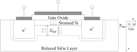
Figure 2.
Schematic diagram of the strained layer depletion region in a Gaussian box.
The first term on the left side of the above equation represents the electric flux entering the Gaussian box from the upper surface, and the second term represents the total electric flux entering the Gaussian box along the y-direction. The whole edge electric flux entering the Gaussian box is equal to the total ionized charge within the Gaussian box, as shown on the right side of the equation. At the bottom of the depleted region, the potential and electric field are both zero due to the connection with the substrate.
Here, is given by , where is a fitting parameter related to the process and can be obtained through parameter extraction. The expression for can be obtained by replacing with Equation (14) as follows:
The boundary conditions for Equation (23) are . The solution is given by:
The equation represents the built-in voltage, where is the doping concentration of the source/drain region and is the doping concentration of the relaxed layer. In this equation, , represents the Boltzmann constant, , is the temperature, and is the charge of an electron. In the strained Si NMOSFET with the strained Si layer, the surface potential is at the surface of the depletion layer in the relaxed layer. Assuming the strained Si layer is thin, we can approximately treat it as a one-dimensional structure:
where represents the surface potential of the long-channel strained Si NMOSFET.
2.2.2. Threshold Voltage
As shown in Equation (26), the surface potential can be minimized along the y-direction. The surface potential at is referred to as the threshold surface potential, and the corresponding gate-source voltage is the threshold voltage. By taking the derivative of Equation (26) with respect to y and finding the zero-crossing point, the surface potential at that point will be the minimum surface potential:
When , substituting this condition into Equation (27) and rearranging, we can obtain:
where . In the expression for , the first term in the numerator can be attributed to the short-channel effect (SCE), which represents the influence of the change in channel length on the threshold voltage when is constant. The second term in the numerator can be attributed to the drain-induced barrier lowering (DIBL) effect, which represents the influence of the change in on the threshold voltage as the channel length varies; then, . Considering the impact of the process, we introduce process parameters [14] , , , , , and , which are obtained through parameter extraction. Therefore, the influences of the SCE and DIBL effect on the threshold voltage can be expressed as:
where in Equation (29), is substituted for , , and .
2.3. The Influence of Narrow-Channel Effect on Threshold Voltage
As shown in Figure 3, in the strained Si NMOSFET device process, there exists a conical oxide transition region between the thin gate oxide layer and the thick field oxide layer, which is referred to as a bird’s beak. When the gate voltage is applied, a gate-controlled depletion region is formed at the edge transition region of the device. The total additional depletion charge caused by the gate voltage at the device edge is ( for each edge). If the channel width W of the device is much larger than the depletion layer width, caused by the gate and the additional depletion charge caused by the gate voltage can be neglected compared to the total depletion charge . However, if W is comparable to , the extra charge cannot be ignored, resulting in an increase in the threshold voltage. The increment of threshold voltage is given by , which means that as W decreases, while L remains constant, increases. To facilitate circuit simulation, different approximations are made for the shape of the depletion region. It is found that is inversely proportional to the device width W and directly proportional to the thickness of the gate oxide layer and the surface potential under strong inversion conditions. Further considerations are given to the substrate bias and the specific process effects, resulting in the development of a semi-empirical model:
and are process-fitting parameters, which are obtained through parameter extraction.
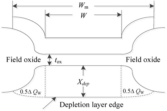
Figure 3.
Cross-sectional diagram of a narrow-channel device in the width direction.
2.4. Complete Threshold Voltage Model
Based on the analysis of threshold voltage in long channel devices, the influences of substrate bias, short-channel effect, drain-induced barrier lowering effect, and narrow-channel effect on threshold voltage were studied. Considering all the factors related to threshold voltage, the complete threshold voltage of a strained Si NMOSFET is determined as:
Among them, the expressions for , , , and are given by Equations (22) and (29)–(31), respectively. By substituting these expressions into Equation (32), we can obtain the complete expression for the threshold voltage of a strained Si NMOSFET as:
3. Tunneling Current Model
When MOSFET devices are scaled down proportionally, tunneling current significantly deteriorates the devices’ performances. To illustrate the impact of tunneling current, it is further explained through Figure 4, Figure 5 and Figure 6. Figure 4 depicts the device’s structural model, while Figure 5 and Figure 6 illustrate the principles of tunneling current and the composition of tunneling current, respectively.
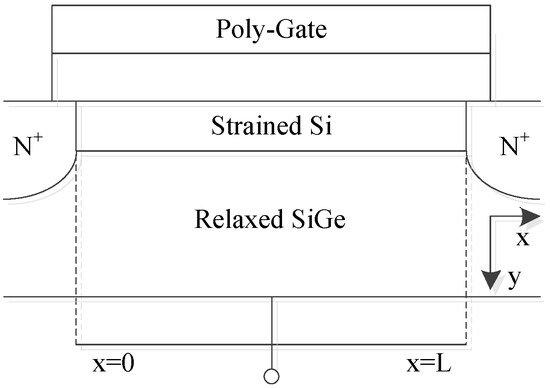
Figure 4.
Schematic diagram of a strained Si/SiGe MOSFET’s structure.
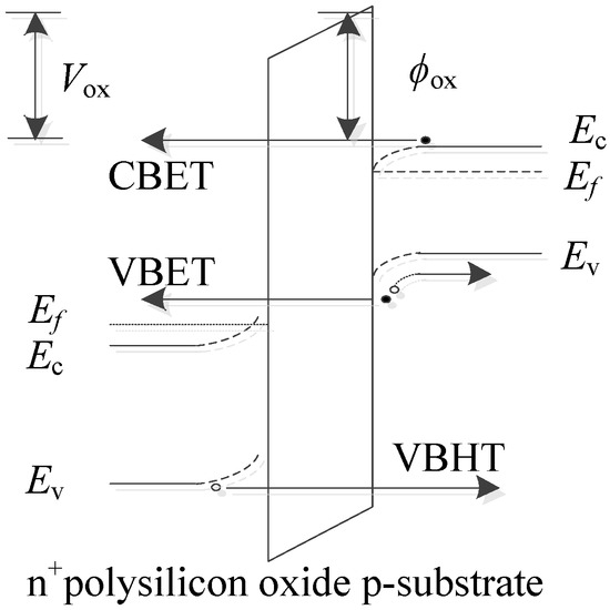
Figure 5.
Subthreshold characteristics of tunneling current.
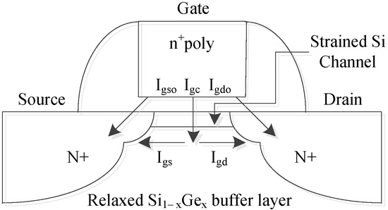
Figure 6.
Composition of tunneling current.
There are three direct tunneling mechanisms in strained silicon MOSFET devices: (1) electron tunneling from the strained silicon conduction band to the gate conduction band (CBET), (2) hole tunneling from the strained silicon valence band to the gate valence band (VBET), and (3) hole tunneling from the strained silicon valence band to the gate conduction band (VBHT).
However, in a strained silicon device with a Poly-Si/SiO2/SSi system, electrons cannot tunnel from the valence band to the conduction band, and holes also cannot tunnel. Therefore, the VBET and VBHT current components are negligible and can be ignored. The gate direct tunneling current in a strained silicon MOSFET device is mainly due to CBET and can be modeled as such [15]:
where represents the direct tunneling current density, represents the barrier height, represents the oxide layer thickness, and A and B are physical parameters with values of and , respectively. Here, represents the Planck constant, and represents the effective mass of electrons in the strained silicon conduction band. Therefore, when assuming , the gate tunneling current at the point can be approximated as:
In the equation, represents the gate tunneling current density at ; , where is an adjustment parameter with a default value of 1; represents the gate-to-source voltage at ; . If the gate leakage current is much smaller than the drain current, then:
In Equation (36), an approximate form is used to describe the characteristics of small-sized devices. This approximation is correct and reasonable when the value is very small or huge.
To more accurately represent tunneling current, the total gate tunneling current can be expressed in integral form as:
According to the mathematical definition of the average value, , the current intensity is equal to the product of current density and area. From Equation (37), we can obtain . For the method of integrating to solve tunneling current, its physical interpretation is that the total current intensity is the product of the gate oxide interface area and the average current density passing through the interface. Here, represents the gate tunneling current density at position .
By using Equations (35) and (36) and the integral formula , if we let , where , we can obtain the total gate tunneling current as:
Combining Equation (33), we can obtain the complete tunneling current model for strained Si devices under small-size effects.
4. Simulation Experiment
4.1. Experimental Parameters
The comprehensive threshold voltage compact physical model is based on strained Si NMOSFETs, and the relevant process parameters are extracted using the corresponding parameter extraction software. The units and specific parameter values of these process parameters are shown in Table 1.

Table 1.
Parameter extraction results.
To demonstrate the correctness of the tunneling current model, devices with gate lengths ranging from 40 nm to 90 nm were selected for experimentation. Table 2 shows the physical parameters of these devices.
Table 2.
Physical parameters.
To comply with the MOSIS deep submicron minimum transistor sizing design rules [16], for a gate length at a technology node, the width of the NMOSFET is set as . In the present study, the width ratio of is set to 2.20 for all technology nodes and kept constant. Therefore, the width of the PMOSFET is . Table 3 displays the BSIM4 MOSFET model parameters AIGSD, BIGSD, CIGSD, AIGC, BIGC, and CIGC used for calculating the gate tunneling current.
Table 3.
The BSIM4 model parameters.
4.2. Experimental Results
Simulations were conducted on the gate and drain currents of an NMOSFET and a PMOSFET under certain bias conditions. The results for the NMOSFET are shown in Figure 7, Figure 8, Figure 9 and Figure 10, while the results for the PMOSFET are shown in Figure 11, Figure 12, Figure 13 and Figure 14. Since the trend of gate tunneling current variation is similar between NMOSFETs and PMOSFETs, in this article, we only used an NMOSFET as an example to illustrate the changes in gate tunneling current for the two different gate states [17].
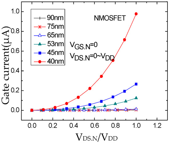
Figure 7.
Gate current at VGS.N = 0.
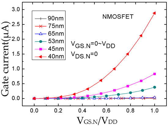
Figure 8.
Gate current at VDS.N = 0.
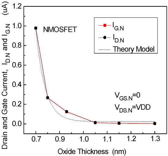
Figure 9.
Trends for VGS.N = 0 and VDS.N = VDD.
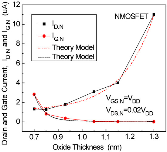
Figure 10.
Trends for VGS.N = VDD and VDS.N = 0.02 VDD.
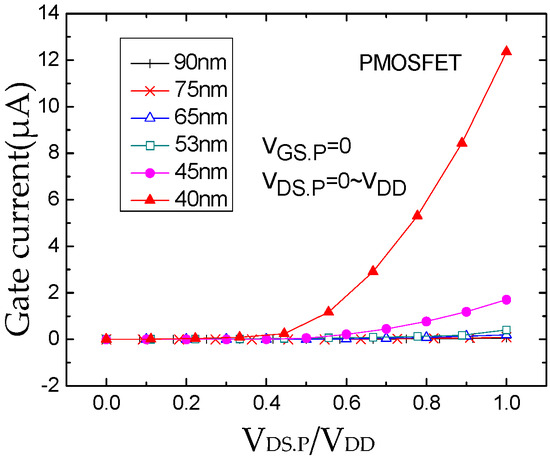
Figure 11.
Gate current at VGS.P = 0.
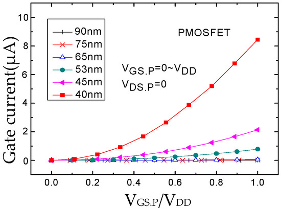
Figure 12.
Gate current at VDS.P = 0.
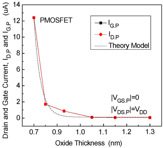
Figure 13.
Trends for VGS.P = 0 and VDS.P = VDD.
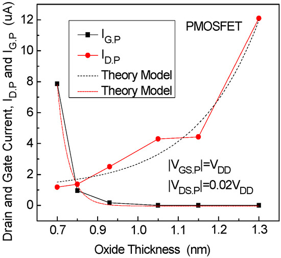
Figure 14.
Trends for VGS.P = VDD and VDS.P = 0.02 VDD.
The simulation results for the NMOSFET and the PMOSFET under two different gate states are shown in Figure 7, Figure 8, Figure 9 and Figure 10. Figure 7 displays the simulation results for the NMOSFET biased in and . From the figures, it can be observed that the gate tunneling current for devices with gate lengths ranging from 90 nm to 65 nm remains nearly constant as the normalized drain-source voltage varies from 0 to 1.0 V. However, for devices with gate lengths ranging from 53 nm to 40 nm, the gate tunneling current exhibits an apparent exponential increase. As the gate length decreases, i.e., as the oxide layer thickness becomes thinner, the gate tunneling current increases more rapidly. With a reduction in gate oxide layer thickness, the gate tunneling current increases from 10−9 A to 10−6 A, approximately three orders of magnitude, for devices with gate lengths ranging from 90 nm to 40 nm. Figure 8 depicts the simulation results for an NMOSFET under another gate state, and , illustrating a similar conclusion. However, the gate tunneling current is greater at compared to .
Figure 11 depicts the contour plot of gate current () and drain current () or the NMOSFET biased at gate state and drain state . For all devices with oxide thickness ranging from 0.7 nm to 1.3 nm under this gate state, both the rectangular-point line representing and the circular-point line describing exhibit similar trends. The magnitude of the drain current is approximately equal to the gate current . The dashed line represents the theoretical variation curve obtained from Equation (38) of the model, which matches the exponential increase observed in the simulation results. This confirms the effectiveness of the proposed model (Equation (38)). The drain current of devices with gate lengths ranging from 90 nm to 40 nm also increases by approximately three orders of magnitude due to the influence of gate tunneling current, as indicated in Figure 7.
In Figure 12, the NMOSFET is biased at gate state and , and is operating in the linear bias region. The simulation results show that, for all devices with oxide thickness ranging from 0.7 nm to 1.3 nm, the circular-point line representing and the rectangular-point line representing exhibit inverse variations, consistent with the model (Equation (38)). The two dashed lines in Figure 12 represent the theoretical results obtained from the model. Notably, for gate lengths ranging from 90 nm to 53 nm, the gate current is significantly smaller than the drain current . For the 45 nm gate length device, the values of and are approximately equal, while for the 40 nm gate length device, is smaller than . These experimental results align with the derived model and support the conclusions drawn from Equation (38). Figure 9, Figure 10, Figure 13 and Figure 14 show the experimental results for the PMOSFET corresponding to the two gate states of the NMOSFET, which are similar to the NMOSFET results and are not further elaborated in the article.
5. Conclusions
In this article, we focus on strained Si NMOSFET devices. We investigate the influences of substrate bias, short-channel effect, and drain-induced barrier lowering effect on threshold voltage, based on the gradual channel approximation and a quasi-two-dimensional Poisson equation. The influence of narrow-channel effect is also studied in detail, and a comprehensive physical model for the threshold voltage is established. The threshold voltage-related parameters are extracted through experiments. Subsequently, the influences of short-channel effect, narrow-channel effect, drain-induced barrier lowering effect, and substrate bias on threshold voltage are discussed in detail. When the drain-source voltage is biased at , the short-channel effect and drain-induced barrier lowering effect cause a threshold voltage shift of 18.57%; a change in channel width results in a threshold voltage shift of 2.75% (as shown in Figure 15); and when the substrate bias is set to , the threshold voltage shifts by 27.22%. Based on the threshold voltage model in this article, we explore the tunneling current in off-state, and provide the experimental results. Future research should involve establishing corresponding models for other structures and smaller-sized devices. The developed physical models for the threshold voltage and tunneling current of strained Si NMOSFETs provide important references for the analysis and design of strained Si large-scale integrated circuits.
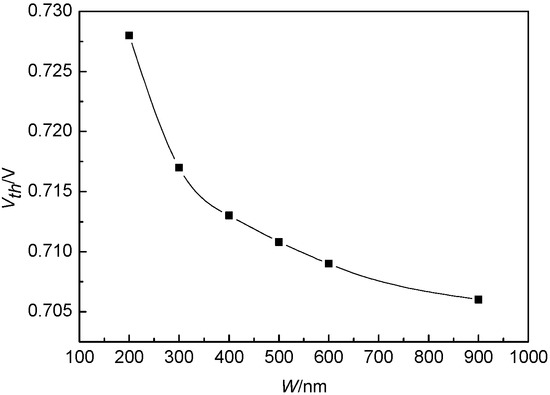
Figure 15.
The variation in threshold voltage with channel width.
Author Contributions
Conceptualization, Z.Z. and C.Z.; methodology, C.Z. and T.W.; software, Z.Z. and T.W.; validation, Z.Z., T.W. and C.Z.; formal analysis, C.Z.; investigation, T.W.; resources, C.Z. and T.W.; data curation, Z.Z.; writing—original draft preparation, Z.Z. and T.W.; writing—review and editing, Z.Z.; visualization, M.W. and Y.X.; supervision, Z.Z.; project administration, Z.Z.; funding acquisition, Q.F. and T.W. All authors have read and agreed to the published version of the manuscript.
Funding
This research was funded by the Fujian Provincial Key Laboratory of Higher Education Open Research Projects, grant number Xnzz1905.
Institutional Review Board Statement
Not applicable.
Informed Consent Statement
Not applicable.
Data Availability Statement
http://bsim.eecs.berkeley.edu (accessed on 11 July 2023).
Acknowledgments
The authors would like to acknowledge financial support provided by the Opening Project of Key Laboratory of Microelectronic Devices & Integrated Technology, Institute of Microelectronics, Chinese Academy of Sciences.
Conflicts of Interest
The authors declare no conflict of interest.
Abbreviations
| Abbreviation | Full Name |
| Si | Silicon |
| NMOSFET | N-channel metal-oxide-semiconductor field-effect transistor |
| MOSFET | Metal-oxide-semiconductor field-effect transistor |
| AC/DC | Alternating current/direct current |
| DIBL | Drain-induced barrier lowering |
| SiGe | Silicon germanium |
| Ge | Germanium |
| SSi | Strained silicon |
| PMOSFET | P-channel metal-oxide-semiconductor field-effect transistor |
| BSIM | Berkeley short-channel IGFET model |
References
- O’Neill, A.G.; Antoniadis, D.A. Deep submicron CMOS based on silicon germanium technology. IEEE Trans. Electron Devices 1996, 43, 911–918. [Google Scholar] [CrossRef]
- Arimoto, K.; Fujisawa, T.; Namiuchi, D.; Onogawa, A.; Sano, Y.; Izumi, D.; Yamanaka, J.; Hara, K.O.; Sawano, K.; Nakagawa, K. Dependences of the hole mobility in the strained Si pMOSFET and gated Hall bars formed on SiGe/Si(110) on the channel direction and the strained Si thickness. J. Cryst. Growth 2021, 571, 126246. [Google Scholar] [CrossRef]
- Wang, G.-Y.; Zhang, H.-M.; Wang, X.-Y.; Wu, T.-F.; Wang, B. Two-dimensional threshold voltage model of sub-100 nm strained-Si/SiGe nMOSFET. Acta Phys. Sin. 2011, 60, 077106. [Google Scholar] [CrossRef]
- Qu, J.T.; Zhang, H.M.; Qin, S.S.; Xu, X.B.; Wang, X.Y.; Hu, H.Y. Study of physically modeling for small-scaled strained Si nMOSFET. Acta Phys. Sin. 2011, 60, 098501. [Google Scholar]
- Hao, M.R.; Hu, H.Y.; Liao, C.G.; Wang, B.; Zhao, X.H.; Kang, H.Y.; Su, H.; Zhang, H.M. The Effect of γ-ray Total Dose Irradiation on the Gate Tunneling Current of Uniaxial Strain Si Nanoscale n-type Metal Oxide Semiconductor Field Effect Transistor. Acta Phys. Sin. 2017, 66, 402–410. [Google Scholar]
- Chandrasekaran, K.; Zhou, X.; Ben Chiah, S.; See, G.H.; Rustagi, S.C. Implicit Analytical Surface/Interface Potential Solutions for Modeling Strained-Si MOSFETs. IEEE Trans. Electron Devices 2006, 53, 3110–3117. [Google Scholar] [CrossRef]
- Sajjad, R.N.; Chern, W.; Hoyt, J.L.; Antoniadis, D.A. Trap assisted tunneling and its effect on subthreshold swing of tunnel field effect transistors. IEEE Trans. Electron Devices 2016, 63, 4380–4387. [Google Scholar] [CrossRef]
- Suzuki, K.; Sudo, R.; Nagase, M. Estimating Lateral Straggling of Impurity Profiles of Ions Implanted Into Crystalline Silicon. IEEE Trans. Electron Devices 2001, 48, 2803–2807. [Google Scholar] [CrossRef]
- El Kashlan, R.Y.; Abd El Hamid, H.; Ismail, Y.I. Two-dimensional models for quantum effects on short channel electrostatics of lightly doped symmetric double-gate MOSFETs. IET Circuits Dev. Syst. 2018, 12, 341–346. [Google Scholar] [CrossRef]
- Arora, N. MOSFET Modeling for VLSI Simulation, 1st ed.; Springer: New York, NY, USA, 2007; pp. 12–68. [Google Scholar]
- Xu, S.L.; Xie, M.X.; Zhang, Z.F. SiGe Microelectronics Technology, 1st ed.; National Defense Industry Press: Beijing, China, 2007; p. 8. [Google Scholar]
- Ma, J.L.; Zhang, Y.; Fu, Z.F.; Zhang, H.M. Valence band structure of biaxial strained Germanium for hole transport calculation. Mol. Phys. 2022, 120, e2074561. [Google Scholar] [CrossRef]
- Yannis, T.; Colin, M. Operation and Modeling of the MOS Transistor, 3rd ed.; Oxford University Press: New York, NY, USA, 2011; pp. 600–638. [Google Scholar]
- Deen, M.; Jamal, Z.; Yan, X. Substrate bias effects on drain-induced barrier lowering in short channel PMOS devices at 77 K. IEEE Trans. Electron Devices 1990, 37, 1707–1713. [Google Scholar] [CrossRef]
- Mondal, I.; Dutta, A.K. An Analytical Gate Tunneling Current Model for MOSFETs Having Ultrathin Gate Oxides. IEEE Trans. Electron Devices 2008, 55, 1682–1692. [Google Scholar] [CrossRef]
- Mukhopadhyay, S.; Raychowdhury, A.; Roy, K. Accurate estimation of total leakage current in scaled CMOS logic circuits based on compact current modeling. In Proceedings of the DAC2003, Anaheim, CA, USA, 9 July 2003. [Google Scholar]
- Zhao, Z.; Wu, T.; Li, J.; Wang, Q.; Han, W. Gate Tunneling Current Model of Scaled Strained Si n -MOSFET with Drain Induced Barrier Lowering Effects. J. Nanoelectron. Optoelectron. 2017, 12, 724–730. [Google Scholar] [CrossRef]
Disclaimer/Publisher’s Note: The statements, opinions and data contained in all publications are solely those of the individual author(s) and contributor(s) and not of MDPI and/or the editor(s). MDPI and/or the editor(s) disclaim responsibility for any injury to people or property resulting from any ideas, methods, instructions or products referred to in the content. |
© 2023 by the authors. Licensee MDPI, Basel, Switzerland. This article is an open access article distributed under the terms and conditions of the Creative Commons Attribution (CC BY) license (https://creativecommons.org/licenses/by/4.0/).