Abstract
In this paper, a first-of-a-kind mixed-mode universal filter employing three VDBAs and three passive components, is proposed. The filter operates in all four modes and provides all five filter responses, namely voltage-mode (VM), current-mode (CM), trans-impedance-mode (TIM), or trans-admittance-mode (TAM). Additionally, the same filter topology can also work as a CM single-input-multi-output (SIMO) filter. A state-of-the-art comparison of various ‘voltage differencing’ variants of the voltage differencing buffered amplifier (VDBA)-based SIMO/MISO (single-input-multi-output/multi-input-single-output)-type biquad filters further highlight the significance of the presented research. In the proposed no passive component matching is required for generating the filter responses. The filter circuit also provides inbuilt tunability of the quality factor independent of the pole frequency. The non-ideal frequency dependent gain and component sensitivity analyses of the filter were also performed. The Silterra Malaysia process design kit (PDK) is employed to design and validated the proposed VDBA-based filter using the Cadence design software. The simulation results closely follow the theoretical predictions. To further verify the practical feasibility of the proposed filter, an experimental evaluation is also completed. The VDBA-based filter is implemented using off-the-shelf operational transconductance amplifiers Intersil CA3080, Texas Instruments LF356 op-amp, and Analog Devices AD844s. The filter is designed for a characteristic frequency of 100 kHz. The time and frequency domain measurement results indicate the proper functioning of the filter.
1. Introduction
Analog frequency filters are an important component of signal processing system. They are employed in instrumentation systems, communication systems, speech processing, sensor data preprocessing, data acquisition systems, etc. [1,2,3]. The active element-based filters are the most employed as they have advantages in terms of chip area, low-power operation, tunability, and compatibility [1,2]. In present day complex signal processing systems, as the design complexity of the system is increasing to achieve high performance, both current-mode and voltage-mode signal processing circuits are employed in a single system. In order to connect the current-mode output to a voltage-mode circuit or vice versa, trans-admittance and trans-impedance stages are required to perform voltage to current (V-I) and I-V conversion. The mixed-mode filters will find application in such a scenario as it will perform the dual task of signal processing and signal conversion simultaneously. One such example is given in reference [4] of a three-way high-fidelity loudspeaker crossover network. The design of mixed-mode universal filters that can provide low-pass (LP), high-pass (HP), band-pass (BP), band-reject (BR), and all-pass (AP) filter responses in CM, VM, TAM, and TIM modes of operation are needed for the mixed signals system architecture [1,2,5,6,7,8,9,10,11,12,13,14,15,16,17,18,19,20]. The popular analog building blocks (ABBs) that are used in the design of active filters include operational transconductance amplifier (OTA) [5], second-generation current conveyor (CCII) [6], differential voltage current conveyor (DVCC) [16], extra current conveyor transconductance amplifier (EXCCTA) [21], differential difference current conveyor (DDCCII) [18], fully differential current conveyor (FDCCII) [15], current differencing buffer amplifier (CDBA) [3], etc. The voltage differencing buffered amplifier (VDBA) is another popular ABB that is very simple in design and versatile in realizing numerous applications [3,22,23,24]. Various ‘voltage differencing’ variants of the VDBA are proposed, such as fully balanced voltage differencing buffered amplifier (FB-VDBA) [25], voltage differencing inverting buffered amplifier (VDIBA) [26,27], fully balanced voltage differencing inverting buffered amplifier (FB-VDIBA) [28], or voltage differencing differential input buffered amplifier (VD-DIBA) [29]. In Table 1 and Table 2, a comparative study is carried out to compare the state-of-the-art SIMO/MISO (single-input-multi-output/multi-input-single-output) voltage differencing unit (VDU)-based biquad filters [25,26,28,29,30,31,32,33,34,35,36,37,38,39,40,41,42,43,44,45,46,47,48,49,50,51,52,53] with here proposed designs. The comparison is made based on the following relevant criteria:
- (i)
- Number of ABBs employed;
- (ii)
- Count of passive components used;
- (iii)
- A requirement of passive components matching condition;
- (iv)
- Application of negative input for response generation;
- (v)
- A requirement of double voltage input for response realization;
- (vi)
- Low output impedance in the case of VM and TIM filters;
- (vii)
- High output impedance in the case of CM and TAM filters;
- (viii)
- Mode of operation;
- (ix)
- Independent tunability of quality factor and filter frequency;
- (x)
- Can realize all five filter responses;
- (xi)
- Test frequency;
- (xii)
- Power dissipation;
- (xiii)
- Supply voltage;
- (xiv)
- Total harmonic distortion (THD).
Reported VDBA-based universal biquadratic filters have three major limitations that severely curtail their application spectrum, which are: (a) non-availability of all five filter responses, (b) the employment of floating passive components, and (c) passive component matching constraints. It can be inferred from the comparative study that out of the 30 designs available in the literature; only 15 can provide all five filter responses in either VM and CM mode [23,26,34,35,36,39,41,42,43,44,45,46,47,48,49,52]. Most importantly, none of the VDU-based filter structures can operate in mixed-mode configuration.
In this research, a first-of-a-kind VDBA-based MISO type mixed-mode universal filter is proposed that can work in all four modes of operation, providing all five filter responses. The proposed structure without any change in the core topology can also function as a SIMO filter providing CM output. The validation of the VDBA and filter is carried out in Cadence design software using Silterra Malaysia PDK. Both simulation and experimental results are in close agreement with the theoretical findings.

Table 1.
Comparative study of various VDU-based SIMO-type biquad filter designs with the proposed filter (Note: NA—not applicable).
Table 1.
Comparative study of various VDU-based SIMO-type biquad filter designs with the proposed filter (Note: NA—not applicable).
| References | (i) | (ii) | (iii) | (iv) | (v) | (vi) | (vii) | (viii) | (ix) | (x) | (xi) (MHz) | (xii) (W) | (xiii) (V) | (xiv) |
|---|---|---|---|---|---|---|---|---|---|---|---|---|---|---|
| [25] | 2-FB-VDBA | 2C + 4R | Yes | NA | NA | Yes | NA | VM/CM | No | No | 1 | – | – | |
| [28] | 2-FB-VDIBA | 2C + 4R | Yes | NA | NA | Yes | NA | VM | No | No | 7.9 | 476 | – | |
| [29] | 2-VD-DIBA | 2C | No | NA | NA | No | NA | VM | No | No | 0.159 | – | 0.76% @ 1.07 V (for HP VM mode) | |
| [33] | 1-ZC-VDBA | 2C | No | NA | NA | NA | No | CM | No | No | 10 | – | ≤10% @ 25 μA (for LP VM mode) | |
| [38] | 1-VDBA | 2C + 3R | No | NA | NA | Yes | NA | VM | No | No | 1.59 | – | – | |
| [39] | 1-VDBA | 2C + 2R | No | NA | NA | NA | No | CM | No | Yes | 0.78 | – | – | |
| [40] | 3-VDBA | 2C | No | NA | NA | Yes | NA | VM | No | No | 0.0469 | – | – | |
| [53] | 2-VD-DIBA | 2C + 2R | No | NA | NA | No | NA | VM | Yes | No | 0.1 | – | ≥1.8% @ 400 mV (for LP VM mode) | |
| This work | 3-VDBA | 2C | No | NA | NA | NA | Yes except (HP) | CM/TAM | Yes | Yes | 16.32 | 5.482 m | ≤4% @ 300 mV (for HP VM mode) |
Table 2.
Comparative study of various VDU-based MISO-type biquad filter designs with the proposed filter (Note: NA—not applicable).
Table 2.
Comparative study of various VDU-based MISO-type biquad filter designs with the proposed filter (Note: NA—not applicable).
| References | (i) | (ii) | (iii) | (iv) | (v) | (vi) | (vii) | (viii) | (ix) | (x) | (xi) (MHz) | (xii) (W) | (xiii) (V) | (xiv) |
|---|---|---|---|---|---|---|---|---|---|---|---|---|---|---|
| [23] | 2-VDBA | 2C | No | Yes | No | Yes | NA | VM | No | Yes | 1.19 | 970 | ±1.5 | ≤1% @ 0.4 V (for BP VM mode) |
| [26] | 1-VDIBA | 2C + R | No | No | NA | No | NA | VM | No | Yes | 1.34 | – | – | – |
| [30] | 2-VDBA | 2C | No | No | NA | Yes | NA | VM | No | No | 0.1 | – | ±0.2 | >1.5% @ 50 mV (for VM mode) |
| [31] | 2-VDIBA | 2C | No | No | NA | No | NA | VM | Yes | No | 2.06 | – | ±0.4 | – |
| [32] | 1-VDBA | 2C + 2R | Yes | No | No | No | NA | VM | No | No | 0.88 | – | ±0.9 | – |
| [34] | 2-VDIBA | 2C | No | No | NA | Yes | NA | VM | No | Yes | 12.9 | 2.8 m | ±0.75 | ≤1% @ 85 mV (for VM mode) |
| [35] | 2-VDIBA | 2C + R | No | Yes | No | Yes | NA | VM | Yes | Yes | 10.1 | 1.14 m | ±0.6 | 0.4% @ 25 mV (for VM mode) |
| [36] | 2-VDBA | 2C | No | No | No | Yes | NA | VM | No | Yes | 56 | 440.6 n | ±0.7 | – |
| [37] | 2-VDBA | 2C | No | No | No | Yes | NA | VM | No | No | 47 | – | – | – |
| [41] | 1-VD-DIBA | 2C + R | Yes | No | Yes | Yes | NA | VM | No | Yes | – | – | ±2 | – |
| [42] | 1-VDIBA | 2C | No | No | No | No | NA | VM | No | Yes | 1.59 | – | ±0.9 | 3.15% @ 50 mV (for BP VM mode) |
| [43] | 1-VDBA | 2C | No | No | No | Yes | NA | VM | No | Yes | 0.766 | – | – | – |
| [44] | 2-VDBA | 2C | No | Yes | No | Yes | NA | VM | No | Yes | 1.16 | – | ±1.5 | >3.15% @ 0.8 V (for BP VM mode) |
| [45] | 2-VDBA | 2C | No | Yes | No | Yes | NA | VM | No | Yes | 10.16 | – | ±1.5 | ≤4% @ 28 mV (for VM mode) |
| [46] | 2-VD-DIBA | 2C | No | No | Yes | Yes | NA | VM | No | Yes | 0.1563 | – | ±5 | – |
| [47] | 2-VDBA | 2C | No | Yes | No | Yes | NA | VM | No | Yes | 22 | 750 | ±0.75 | ≥2% @ 50 mV (for BP VM mode) |
| [48] | 1-VDBA | 2C + R | No | Yes | No | No | NA | VM | No | Yes | – | – | ±1.5 | – |
| [49] | 1-VDBA | 2C + R | No | Yes | No | No | NA | VM | Yes | Yes | 19.49 | 360 | ±0.75 | – |
| [50] | 2-VDIBA | 2C + R | No | No | No | No | NA | VM | Yes | No | – | – | ±0.6 | – |
| [51] | 2-VD-DIBA | 2C + 2R | No | No | No | No | NA | VM | Yes | No | 0.3093 | – | ±5 | >4% @ 90 mV (for BP VM mode) |
| [52] | 2-VDBA | 2C | No | Yes | No | Yes | NA | VM | No | Yes | 0.05 | – | ±5 | 2.98% @ 50 mV (for BP VM mode) |
| [53] | 2-VD-DIBA | 2C + 2R | Yes | No | No | Yes | NA | VM | Yes | Yes | 0.1 | – | – | – |
| [54] | 3-VDBA | 2C + 2R | No | No | No | Yes | Yes | VM, TAM | Yes | Yes | 7.2 | 5.47 m | ±1.25 | ≤6% @ 250 mV (for BP VM mode) |
| This work | 3-VDBA | 2C + R | No | No | No | Yes | Yes | VM, CM, TIM, TAM | Yes | Yes | 16.34 | 5.482 m | ±1.25 | ≤4% @ 350 mV (for HP VM mode) |
2. Voltage Differencing Buffered Amplifier (VDBA)
The VDBA simply is a cascade connection of a voltage buffer and an operational transconductance amplifier (OTA). The voltage-current relationship of the VDBA is presented in Equation (1) and the functional block representation is given in Figure 1a.
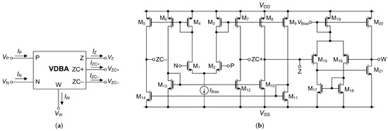
Figure 1.
(a) Block diagram and (b) CMOS implementation of VDBA.
The VDBA is a six-terminal device, of which CMOS implementation is shown in Figure 1b. The first transconductance amplifier stage is built by the transistors M1–M14. The output current of the transconductance amplifier depends on the difference in voltage between P and N terminals. If operation in saturation region is assumed and ratio for transistors M1 and M2 are made identical then the output current of the OTA is given by Equation (2): The voltage follower forms the second stage of the VDBA designed using transistors M15–M21.
where the transconductance parameter , W is the effective channel width, L is the effective length of the channel, is the gate oxide capacitance per unit area, and is the carrier mobility.
3. Proposed Universal Filter
The proposed filter shown in Figure 2 utilizes three VDBAs and three passive components. The filter provides all five filter responses in all four modes of operation in MISO configuration. The filter can also be used in SIMO configuration wherein it provides CM responses. The MISO filter has the following features: (i) ability to operate in all four modes of operation, (ii) low output impedance for VM/TIM and high input impedance for CM/TAM, (iii) no passive component matching required, (iv) no need for inverting inputs for response realization, and (v) inbuilt tunability of quality factor independent of pole frequency.
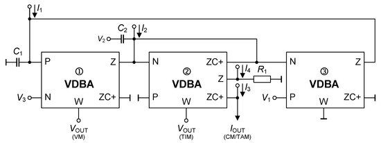
Figure 2.
Proposed MISO mixed-mode universal filter.
3.1. Operation in VM and TAM Modes
In VM, the input voltage () is applied according to Table 3 to obtain all five filter responses, namely LP, BP, HP, BR, and AP. Equations (3) and (4) give the transfer function of the VM and TAM, while Equations (5) and (6) give the expression for the characteristic frequency and quality factor. The input current () is set to zero.
Table 3.
Input voltage excitation sequence.
3.2. Operation in Current- and Trans-Impedance-Modes
In CM mode, the input voltage () is set to zero and input currents are applied according to Table 4 to obtain all five filter responses. Equations (7) and (8) give the transfer functions of the CM modes.
Table 4.
Input current excitation sequence.
In the current- and trans-impedance-modes of operation, only three input currents will be used. For CM, currents , , and for TIM currents , , will be applied, respectively. In addition, to realize AP response with double magnitude is required. It can be easily generated by applying two currents of equal magnitude at the input node without requiring any additional hardware. Furthermore, the gain of the TIM response can be adjusted using the resistor .
3.3. SIMO Filter Configuration
Figure 3 shows the SIMO filter topology. It can be seen from the figure that the core circuit remain unchanged and the resistor is no longer required leading to resistorless implementation. The only drawback is the availability of the HP output through the capacitor. The HP current can be sensed using a current follower. In the SIMO configuration, the filter can function in CM mode by providing all five filter responses.
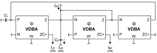
Figure 3.
Proposed SIMO dual-mode universal filter.
For the current-mode of operation, is set to zero and current is applied to the filter topology. The transfer functions in the CM are given in Equations (9)–(13), while a corresponding quality factor and pole frequency are given in Equations (14) and (15).
Note that the BR and AP responses can be obtained by summing the LP, HP, and BP currents, and .
4. Non-Ideal Analysis
The mismatch between current mirrors, process variation and the device mismatch between the MOS transistors results in variation in the frequency dependent voltage and current transfer gains of the VDBA. This change in the gain from the ideal value of unity results in the deviation in the center frequency and quality factor of the filter. The effect of frequency dependent non-deal voltage and current transfer gains is analyzed in this section. The () denotes the frequency dependent non-ideal voltage transfer gain and represents the transconductance transfer gain of the OTA. Considering the effect of the non-ideal gains the V-I characteristics of the VDBA will be modified as given in Equations (16)–(18), where and , for , which refers to the number of VDBAs. Here, denote voltage tracking error, and denote transconductance errors of the VDBA.
The modified transfer function and expressions for center frequency and quality factor including the non-ideal effect is given in Equations (19)–(24) for the MISO filter. The non-idealities result in deviations from the expected value.
The non-ideal expressions of the filter transfer function for the CM SIMO filter are given as follows:
The sensitivities of and Q with respect to the non-ideal gain and passive elements are calculated. Equations (28)–(30) indicate identical sensitivities for the MISO mixed-mode universal filter and CM SIMO filter.
The sensitivities are not greater than one, which is desired.
5. Parasitic Analysis
The block diagram presented in Figure 4 shows the various parasitic impedance associated with different terminals of the VDBA. The parasitic resistances and capacitance appear in parallel with the P, N, and Z terminals. The low impedance W terminal has a resistance in series with the inductance. For the frequency of interest, the inductance effect can be ignored. The denominator of the filter transfer function is modified in the presence of the parasitic effect as given in Equation (31).
where and .
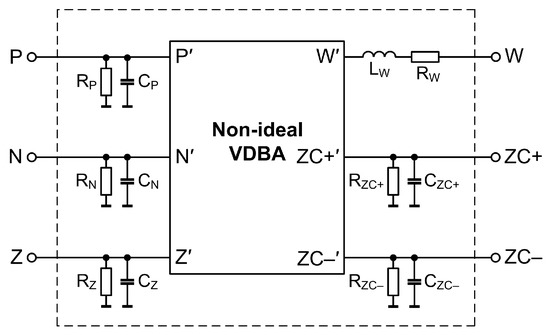
Figure 4.
Non-ideal model of VDBA.
If and are made greater, the the expression for and will be simplified as given below.
6. Simulation Results
To validate the performance of the designed VDBA-based mixed-mode universal filter, it was designed and simulated in Silterra Malaysia technology using Cadence Virtuoso software. The supply voltages ±1.25 V are used. The width and length of the MOS transistors in Figure 1b are given in Table 5, while the design metrics of the VDBA active block are listed in Table 6.
Table 5.
Width and length of the MOS transistors.
Table 6.
Performance metrics of the VDBA.
The developed filter is designed for a pole frequency of 16.631 MHz by selecting component values as , , and . It must be mentioned that results provided for the filter are pre-layout results considering the nominal values as provided in the Silerra Malaysia PDK. The proposed filter is suitable for wide variety of applications in industrial signal processing and wireless communication, etc. The frequency-domain responses of the filter in all four modes are presented in Figure 5, Figure 6, Figure 7 and Figure 8. To test the quality factor tuning independent of the frequency BP response is plotted for different values of the bias current . It can be inferred from Figure 9 that the quality factor can be tuned without disturbing the frequency.
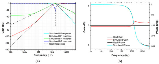
Figure 5.
Frequency response of the MISO VM Filter: (a) LP, BP, HP, and BR (b) AP.
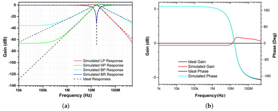
Figure 6.
Frequency response of the MISO CM Filter: (a) LP, BP, HP, and BR (b) AP.
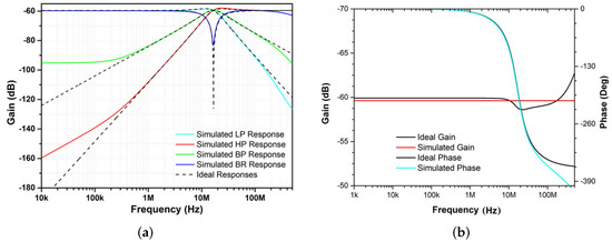
Figure 7.
Frequency response of the MISO TAM Filter: (a) LP, BP, HP, and BR (b) AP.
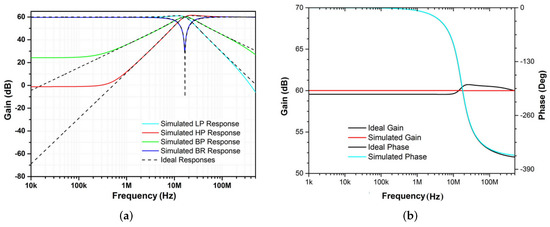
Figure 8.
Frequency response of the MISO TIM Filter: (a) LP, BP, HP, and BR (b) AP.
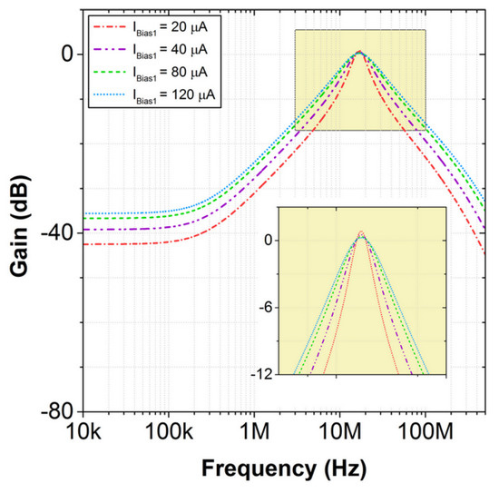
Figure 9.
Quality factor tuning for CM BP filter.
As the OTA offset current can cause frequency and phase deviation in the designed filter, Monte Carlo analysis is carried out for 200 runs to obtain an accurate measure of the offset current at the (Z, ZC + ) terminals of the OTA. The of OTA is set at 120 A. The results show minimum offset current A, maximum offset current A, mean offset current A and standard deviation A. To verify the signal processing capability of the filter, transient analysis is performed for BP responses in the VM and CM mode. In VM, a sinusoidal signal of 16.6 MHz frequency and 200 mV peak-to-peak is applied at the input and the output waveform is observed as given in Figure 10a. In CM, a sinusoidal signal of 16.6 MHz frequency and 100 A peak-to-peak is applied and the output waveform is presented in Figure 10b. It can be observed that the filter functions correctly.
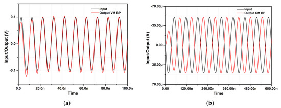
Figure 10.
Transient analysis result for BP filter: (a) VM MISO and (b) CM MISO configurations.
To study the effect of process spread on the designed filter, Monte Carlo analysis is done for 200 runs for VM BP and CM AP configurations as presented in Figure 11a,b. It can be deduced from the figures that there is no large variation in the pole frequency of the filter due to process variations.
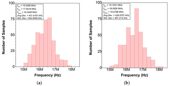
Figure 11.
Monte Carlo analysis results: (a) BP of VM MISO, (b) AP of CM MISO configurations.
The THD of the proposed filter for LP, HP, and BP responses is plotted for different input signal amplitudes for VM, as shown in Figure 12a. The THD plot for CM-BP/LP is presented in Figure 12b. As per the IEEE Std 519-2014 [55] the THD of the filter remains within acceptable limits (≤5%) for a considerable input signal range. Moreover, the THD performance of the filter is at par with other reported mixed-mode filters [10,11,13,14,15,19].
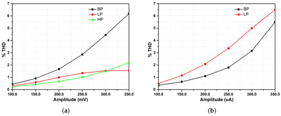
Figure 12.
Total harmonic distortion results: (a) VM-LP, VM-HP, and VM-BP, (b) CM-LP and CM-BP.
The reduction in the frequency of the filter due to the increase in temperature can be ascribed to the decrease in the transconductance of the OTA. The major factors affecting the transconductance are carrier mobility () and threshold voltage (). The carrier mobility dependence on temperature can be modeled by Equation (38):
where stands for the mobility temperature exponent, it is considered constant roughly equal to 1.5. The threshold voltage can be approximated as a linear function of temperature [56,57] given by Equation (39):
here, denotes the threshold voltage temperature coefficient, which varies from −1 mV/C to −4 mV/C and is the reference temperature (300 K). These two Equations exhibit negative temperature dependence and this correlates with the decrease in the filter frequency with temperature as observed in Figure 13. The effect of noise on the performance of the proposed filter is also analyzed. The thermal and flicker noise are present in the bulk CMOS devices, and they effect the performance of the designed filter. Figure 14 gives the plot of the input and output noise for the BP VM filter configuration. At the pole frequency of the filter the input and output noises are found to be 36.2 nV/ and 36.48 nV/, respectively. It can be seen from the figure that the input and output noise are well within the acceptable limits.
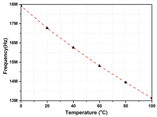
Figure 13.
CM MISO Filter: Variation of filter frequency with temperature.
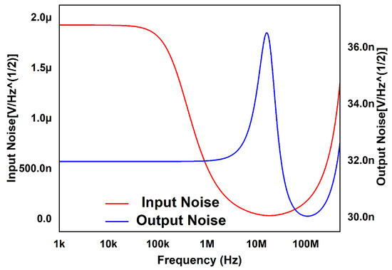
Figure 14.
Input and output noise analysis of VM BP MISO filter configuration.
To verify the CM SIMO filter, it is designed with the exact specifications of the MISO filter. The frequency responses of the filter are shown in Figure 15.
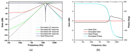
Figure 15.
Frequency response of the CM SIMO Filter: (a) LP, BP, HP, and BR filter (b) AP.
The time domain and THD analysis for the SIMO current-mode filter are presented in Figure 16 and Figure 17. The results validate the correct functioning of the designed filter.
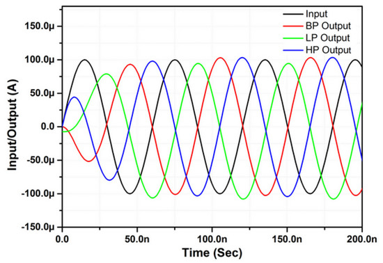
Figure 16.
Transient response of the CM SIMO Filter: LP, HP, and BP.
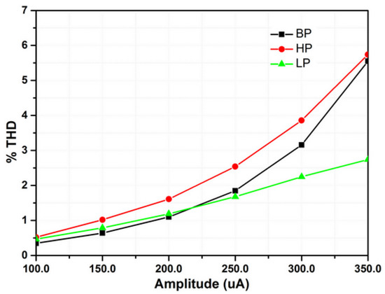
Figure 17.
Total harmonic distortion of CM SIMO filter: CM-HP, CM-LP, and CM-BP.
The Monte Carlo analysis results for the designed CM BP filter response are presented in Figure 18. The frequency response and the static variations in the designed frequency are under acceptable limits.
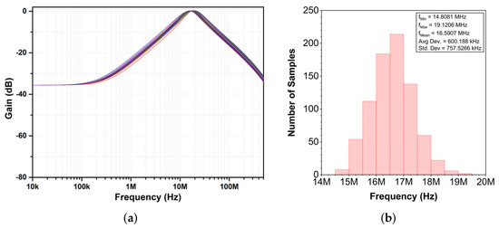
Figure 18.
Monte Carlo analysis of CM SIMO Filter: (a) the results and (b) the corresponding histogram.
To highlight the advantages of the designed filter, it is compared with some exemplary designs of mixed-mode filters, as shown in Table 7. By analyzing the comparison table, it can be observed that the proposed filter structure holds certain advantages over the other similar designs and also performs at par with other designs in terms of power dissipation, supply voltage, and total harmonic distortion, in addition to being the first truly mixed-mode filter based on the VDBA. The authors would like to point out that the recently reported VDBA-based mixed-mode filter designs [54,58] are not truly mixed-mode as they cannot provide all five filter responses in all four modes of operation. Furthermore, in [58] the output currents are not available from high-impedance nodes; hence extra current followers will be needed to extract the currents.
Table 7.
Comparison of the proposed filter with other similar topologies.
7. Experimental Validation
To further verify the correct functioning of the proposed filter circuit and to complement the theoretical and simulation results, detailed experimental analysis is carried out for MISO VM and TAM modes and SIMO CM configuration. The VDBA is built with available integrated circuits (ICs), the Intersil CA3080 OTAs and Texas Instruments LF356 op-amp, as shown in Figure 19. The supply voltages are set ±5 V.
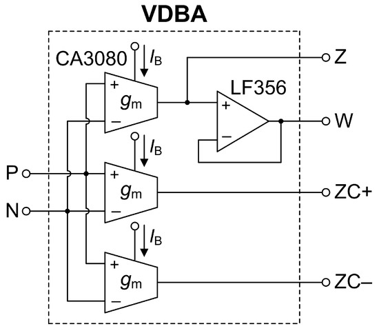
Figure 19.
VDBA implementation using off-the-shelf ICs.
To design the filter for a pole frequency of = 100.27 kHz and , the active component values are selected as of i-th VDBA, i= 1, 2, 3) = 0.63 mA/V (I = 31.5 A), where and is thermal voltage ≅ 25 mV at 27 C. In all measurements, the passive components are chosen as , and . The measured LP, HP, BP, BR, and AP frequency response results of the VM MISO configuration in Figure 2 are given in Figure 20. Figure 21 also presents the measured time-domain responses for LP, HP, BP, and BR filters, when the sinusoidal input signal of an amplitude 100 mV peak-to-peak at 100 kHz is applied. In addition, the measurement of input and output voltage waveforms of the VM AP filter and the FFT analysis results at the output terminal are given in Figure 22, respectively.
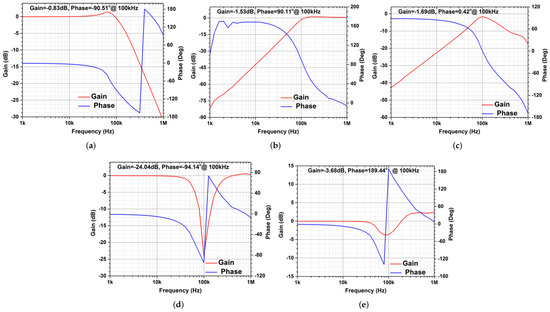
Figure 20.
VM MISO configuration: Measured gain and phase responses of the (a) LP, (b) HP, (c) BP, (d) BR, and (e) AP.
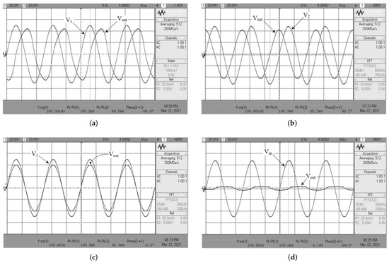
Figure 21.
VM MISO configuration: Measured input and output waveforms of the (a) LP, (b) HP, (c) BP, and (d) BR.
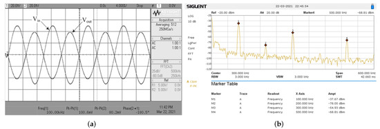
Figure 22.
VM MISO configuration: (a) measured input and output waveforms of the AP filter, (b) its FFT analysis results.
For obtaining the TAM and CM SIMO filter results, two additional Analog Devices AD844s and a converting resistor () are employed to covert current to voltage. The circuit is shown in Figure 23, where the value of is equal to 1 k. Figure 24 shows the measured TAM filtering responses with the same component values as described above for 100.27 kHz and . Next, Figure 25 shows the time-domain responses of the proposed TAM operation for LP, BP, HP, and BR filters. In Figure 26, the measured input and output voltage waveforms of the TAM AP filter and its FFT spectrum analysis are, respectively, given.
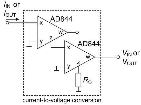
Figure 23.
Voltage to current conversion setup for obtaining TAM and CM SIMO filter results.
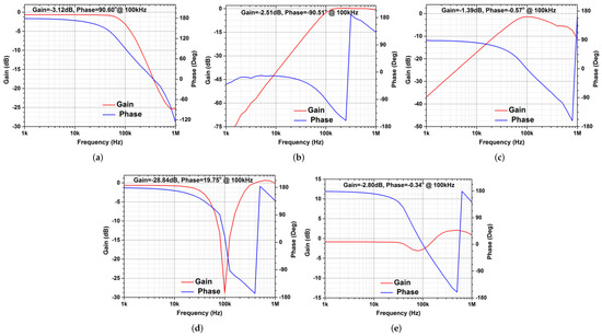
Figure 24.
TAM MISO configuration: Measured gain and phase responses of the (a) LP, (b) HP, (c) BP, (d) BR, and (e) AP.
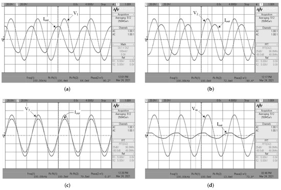
Figure 25.
TAM MISO configuration: Measured input and output waveforms of the (a) LP, (b) HP, (c) BP, and (d) BR.
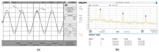
Figure 26.
TAM MISO configuration: (a) measured input and output waveforms of the AP filter, (b) its FFT analysis results.
In the same way, the LP, HP, and BP filter responses of the CM SIMO filter in Figure 3 are presented in Figure 27. In this case, the circuit components are the same as that used in the above design to have the following filter characteristics: 100.27 kHz and . As expected, the experimental results of the CM SIMO configuration are close to the theoretical results.
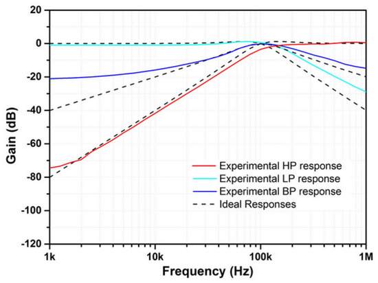
Figure 27.
CM SIMO configuration: Gain responses of the LP, BP, and HP filter.
From the experimental results, it is evident that the proposed filter topologies are practically realizable. The deviation in the measurement results is mainly due to the breadboard circuit implementation. It is expected that, when the filter circuit is fabricated, the behavior of the proposed filter will be very close to the simulation results.
8. Conclusions
In this research, a truly mixed-mode universal filter based on VDBA is proposed. The filter requires three VDBAs, two capacitors, and a resistor for implementation. It provides all five filter responses in all four modes of operation in MISO configuration. A SIMO resistorless CM universal filter can also be derived from the same core arrangement. In MISO configuration, the VM/TIM outputs are available from low impedance nodes and CM/TAM outputs are available from high impedance node leading to cascadability. The filter has a feature of inbuilt tunability as well. The detailed theoretical analysis, non-ideal, and sensitivity analyses are performed to establish the correct functioning of the filter. The VDBA-based filter is designed and validated in Cadence Virtuoso software using Silterra Malaysia PDK. The filter is designed for a characteristic frequency of 16.66 MHz with a ±1.25 V supply. The Monte Carlo analysis shows that the frequency deviation is within acceptable limits. Additionally, the THD is within 5% for a substantial voltage/current input signal range. The experimental validation of the proposed filter is also carried out. The filter is constructed using commercially available ICs. The frequency responses and time-domain results of the filter confirm the correct functioning. The simulation and experimental results are found consistent with the theoretical predictions.
Author Contributions
Conceptualization, M.F., N.H. and S.S.; methodology, M.F.; software, M.F. and S.S.; validation, M.F., S.S. and W.T.; formal analysis, M.F. and N.H.; investigation, M.F.; resources, S.H.M.A.; data curation, M.F. and N.H.; writing—original draft preparation, M.F., N.H. and W.T.; writing—review and editing, M.F., N.H. and W.T.; visualization, M.F. and N.H.; supervision, N.H., S.H.M.A.; project administration, S.H.M.A.; funding acquisition, S.H.M.A. All authors have read and agreed to the published version of the manuscript.
Funding
This research work was funded by University Kebangsaan Malaysia (UKM) under grant (GUP2020-009).
Institutional Review Board Statement
Not applicable.
Informed Consent Statement
Not applicable.
Data Availability Statement
The data presented in this study are available on request from the authors.
Conflicts of Interest
The authors declare no conflict of interest.
Abbreviations and Symbols
The following abbreviations and symbols are used in this manuscript:
| Frequency dependent non-ideal voltage gain | |
| Frequency dependent non-ideal transconductance transfer gains | |
| Carrier mobility | |
| ABB | Active building blocks |
| AP | All-pass |
| BP | Band-pass |
| BR | Band-reject |
| CCII | Second-generation current conveyor |
| CDBA | Current differencing buffer amplifier |
| CFOA | Current feedback operational amplifier |
| CM | Current-mode |
| Gate oxide capacitance per unit area | |
| DDCC | Differential difference current conveyor |
| DDCCII | Differential difference current conveyor |
| DVCC | Differential voltage current conveyor |
| EXCCTA | Extra X current conveyor transconductance amplifier |
| FB-VDBA | Fully balanced voltage differencing buffered amplifier |
| FB-VDIBA | Fully balanced voltage differencing inverting buffered amplifier |
| FDCCII | Fully Differential Current Conveyor |
| Transconductance of the operational transconductance amplifier | |
| HP | High-pass |
| IC | Integrated circuit |
| L | Effective length of the channel |
| LP | Low-pass |
| MCCTA | Modified current conveyor trans-conductance amplifier |
| MISO | Multi input single output |
| MOCCCII | Multi output current controlled current conveyor |
| OTA | Operational transconductance amplifier |
| PDK | Process design kit |
| Q | Quality factor |
| SIMO | Single input multi output |
| TAM | Trans-admittance-mode |
| THD | Total harmonic distortion |
| TIM | Trans-impedance-mode |
| VDBA | Voltage differencing buffered amplifier |
| VD-DIBA | Voltage differencing differential input buffered amplifier |
| VDIBA | Voltage differencing inverting buffered amplifier |
| VDTA | Voltage differencing transconductance amplifier |
| VM | Voltage-mode |
| Threshold voltage | |
| W | Effective channel width |
| ZC-VDBA | Z-copy voltage differencing buffered amplifier |
References
- Mohan, P.A. Current-Mode VLSI Analog Filters: Design and Applications; Springer Science & Business Media: Berlin, Germany, 2003. [Google Scholar] [CrossRef]
- Raut, R.; Swamy, M. Modern Analog Filter Analysis and Design: A Practical Approach; John Wiley & Sons: Hoboken, NJ, USA, 2010. [Google Scholar] [CrossRef]
- Biolek, D.; Senani, R.; Biolkova, V.; Kolka, Z. Active elements for analog signal processing: Classification, review, and new proposals. Radioengineering 2008, 17, 15–32. [Google Scholar]
- Chen, H.P.; Liao, Y.Z.; Lee, W.T. Tunable mixed-mode OTA-C universal filter. Analog Integr. Circuits Signal Process. 2009, 58, 135–141. [Google Scholar] [CrossRef]
- Abuelma’atti, M.T.; Bentrcia, A. A novel mixed-mode OTA-C filter. Frequenz 2003, 57, 157–159. [Google Scholar] [CrossRef]
- Abuelma’atti, M.T.; Bentrcia, A.; Al-Shahrani, S.A.M. A novel mixed-mode current-conveyor-based filter. Int. J. Electron. 2004, 91, 191–197. [Google Scholar] [CrossRef]
- Pandey, N.; Paul, S.K.; Bhattacharyya, A.; Jain, S.B. A new mixed mode biquad using reduced number of active and passive elements. IEICE Electron. Express 2006, 3, 115–121. [Google Scholar] [CrossRef]
- Ibrahim, M.A. Design and analysis of a mixed-mode universal filter using dual-output operational transconductance amplifiers (DO-OTAs). In Proceedings of the 2008 International Conference on Computer and Communication Engineering, Kuala Lumpur, Malaysia, 13–15 May 2008; pp. 915–918. [Google Scholar] [CrossRef]
- Lee, C.N. Multiple-Mode OTA-C Universal Biquad Filters. Circuits Syst. Signal Process. 2010, 29, 263–274. [Google Scholar] [CrossRef]
- Pandey, N.; Paul, S.K.; Bhattacharyya, A.; Jain, S. Realization of Generalized Mixed Mode Universal Filter Using CCCIIs. J. Act. Passiv. Electron. Devices 2010, 5, 279–293. [Google Scholar]
- Pandey, N.; Paul, S.K. Mixed mode universal filter. J. Circuits Syst. Comput. 2013, 22, 1250064. [Google Scholar] [CrossRef]
- Kaçar, F.; Kuntman, A.; Kuntman, H. Mixed-mode biquad filter employing single active element. In Proceedings of the 2013 IEEE 4th Latin American Symposium on Circuits and Systems (LASCAS), Cusco, Peru, 27 February–1 March 2013; pp. 1–4. [Google Scholar] [CrossRef]
- Yeşil, A.; Kaçar, F. Electronically tunable resistorless mixed mode biquad filters. Radioengineering 2013, 22, 1016–1025. [Google Scholar]
- Yuce, E. Fully integrable mixed-mode universal biquad with specific application of the CFOA. AEU-Int. J. Electron. Commun. 2010, 64, 304–309. [Google Scholar] [CrossRef]
- Lee, C.N. Independently tunable mixed-mode universal biquad filter with versatile input/output functions. AEU-Int. J. Electron. Commun. 2016, 70, 1006–1019. [Google Scholar] [CrossRef]
- Tsukutani, T.; Yabuki, N. A DVCC-based mixed-mode biquadratic circuit. J. Electr. Eng. 2018, 6, 52–56. [Google Scholar] [CrossRef]
- Bhaskar, D.R.; Raj, A.; Kumar, P. Mixed-mode universal biquad filter using OTAs. J. Circuits Syst. Comput. 2020, 29, 2050162. [Google Scholar] [CrossRef]
- Lee, C.N.; Yang, W.C. General Mixed-Mode Single-Output DDCC-based Universal Biquad Filter. Int. J. Eng. Res. Technol. (IJERT) 2020, 9, 744–749. [Google Scholar]
- Singh, S.V.; Tomar, R.S.; Chauhan, D.S. A new electronically tunable universal mixed-mode biquad filter. J. Eng. Res. 2016, 2, 1–21. [Google Scholar] [CrossRef]
- Ettaghzouti, T.; Hassen, N.; Besbes, K. Novel multi-input single-output mixed-mode universal filter employing second generation current conveyor circuit. Sens. Circuits Instrum. Syst. Ext. Pap. 2018, 6, 53–64. [Google Scholar] [CrossRef]
- Albrni, M.I.A.; Mohammad, F.; Herencsar, N.; Sampe, J.; Ali, S.H.M. Novel Electronically Tunable Biquadratic Mixed-Mode Universal Filter Capable of Operating in MISO and SIMO Configurations. Inf. MIDEM J. Microelectron. Electron. Compon. Mater. 2020, 50, 189–203. [Google Scholar] [CrossRef]
- Tangsrirat, W. Linearly tunable voltage differencing buffered amplifier. Rev. Roum. Des. Sci. Tech. 2019, 64, 247–253. [Google Scholar]
- Kacar, F.; Yesil, A.; Noori, A. New CMOS realization of voltage differencing buffered amplifier and its biquad filter applications. Radioengineering 2012, 21, 333–339. [Google Scholar]
- Gupta, P.; Pandey, R. A low-power voltage differencing buffered amplifier. Int. J. Circuit Theory Appl. 2019, 47, 1402–1416. [Google Scholar] [CrossRef]
- Biolkova, V.; Kolka, Z.; Biolek, D. Fully balanced voltage differencing buffered amplifier and its applications. In Proceedings of the 2009 52nd IEEE International Midwest Symposium on Circuits and Systems, Cancun, Mexico, 2–5 August 2009; pp. 45–48. [Google Scholar] [CrossRef]
- Pushkar, K.L.; Bhaskar, D.R.; Prasad, D. Voltage-mode new universal biquad filter configuration using a single VDIBA. Circuits Syst. Signal Process. 2014, 33, 275–285. [Google Scholar] [CrossRef]
- Kumari, S.; Gupta, M. New CMOS realization of high performance Voltage Differencing Inverting Buffered Amplifier and its filter application. Analog Integr. Circuits Signal Process. 2017, 92, 167–178. [Google Scholar] [CrossRef]
- Kumari, S.; Gupta, M. A Design and Analysis of Low Voltage FB-VDIBA and Biquad Filter Application. In Proceedings of the 2018 5th International Conference on Signal Processing and Integrated Networks (SPIN), Noida, India, 22–23 February 2018; pp. 301–306. [Google Scholar] [CrossRef]
- Jaikla, W.; Biolek, D.; Siripongdee, S.; Bajer, J. High input impedance voltage-mode biquad filter using VD-DIBAs. Radioengineering 2014, 23, 914–921. [Google Scholar]
- Başak, M.E.; Kacar, F. Ultra-low voltage VDBA design by using PMOS DTMOS transistors. Istanb. Univ. J. Electr. Electron. Eng. 2017, 17, 3463–3469. [Google Scholar]
- Sokmen, O.G.; Tekin, S.A.; Ercan, H.; Alci, M. A novel design of low-voltage VDIBA and filter application. Elektron. Elektrotech. 2016, 22, 51–56. [Google Scholar] [CrossRef][Green Version]
- Bansal, U.; Gupta, M.; Rai, S.K. Resistively compensated and SSF based VDBA offering high GBW and its application as a biquad filter. In Proceedings of the 2017 International Conference on Computer, Communications and Electronics (Comptelix), Jaipur, India, 1–2 July 2017; pp. 221–226. [Google Scholar] [CrossRef]
- Güney, A.; Alaybeyoğlu, E.; Kuntman, H. New CMOS realization of Z copy voltage differencing buffered amplifier and its current-mode filter application. In Proceedings of the 2013 8th International Conference on Design & Technology of Integrated Systems in Nanoscale Era (DTIS), Abu Dhabi, United Arab Emirates, 26–28 March 2013; pp. 68–71. [Google Scholar] [CrossRef]
- Gupta, M.; Srivastava, R.; Singh, U. Low-voltage low-power FGMOS based VDIBA and its application as universal filter. Microelectron. J. 2015, 46, 125–134. [Google Scholar] [CrossRef]
- Kumari, S.; Gupta, M. Design and Analysis of Tunable Voltage Differencing Inverting Buffered Amplifier (VDIBA) with Enhanced Performance and Its Application in Filters. Wirel. Pers. Commun. 2018, 100, 877–894. [Google Scholar] [CrossRef]
- Srivastava, R.; Gupta, O.K.; Kumar, A.; Singh, D. Low-voltage bulk-driven self-cascode transistor based voltage differencing inverting buffered amplifier and its application as universal filter. Microelectron. J. 2020, 102, 104828. [Google Scholar] [CrossRef]
- Mamatov, I.; Özçelep, Y.; Kaçar, F. Voltage differencing buffered amplifier based low power, high frequency and universal filters using 32 nm CNTFET technology. Microelectron. J. 2021, 107, 104948. [Google Scholar] [CrossRef]
- Gupta, P.; Pandey, R. Single VDBA based multifunction filter. Int. J. Control Theory Appl. 2017, 10, 651–661. [Google Scholar]
- Yadav, C.K.; Prasad, D.; Haseeb, Z.; Kumar, M. CM-Biquad filter using single DO-VDBA. Circuits Syst. 2018, 9, 133–139. [Google Scholar] [CrossRef][Green Version]
- Khatib, N.; Biolek, D. New voltage-mode universal filter based on promising structure of voltage differencing buffered amplifier. In Proceedings of the 2013 23rd International Conference Radioelektronika, Pardubice, Czech Republic, 16–17 April 2013; pp. 177–181. [Google Scholar] [CrossRef]
- Pushkar, K.L.; Bhaskar, D.R.; Prasad, D. Voltage-mode universal biquad filter employing single voltage differencing differential input buffered amplifier. Circuits Syst. 2013, 4, 44–48. [Google Scholar] [CrossRef]
- Herencsar, N.; Cicekoglu, O.; Sotner, R.; Koton, J.; Vrba, K. New resistorless tunable voltage-mode universal filter using single VDIBA. Analog Integr. Circuits Signal Process. 2013, 76, 251–260. [Google Scholar] [CrossRef]
- Onjan, O.; Unhavanich, S.; Tangsrirat, W. SFG actualization of general nth-order voltage transfer functions using VDBAs. In Proceedings of the International MultiConference of Engineers and Computer Scientists, Hong Kong, China, 16–18 March 2016; pp. 585–589. [Google Scholar] [CrossRef]
- Ismael, A.R. CMOS Implementation Of VDBA To Design Symmetric Filters. J. Multidiscip. Eng. Sci. Technol. (JMEST) 2016, 3, 4178–4181. [Google Scholar]
- Ismael, A.R. The applications employed to design a new kind of filter using the active element (VDBA). Kirkuk Univ. J. Sci. Stud. 2016, 11. [Google Scholar] [CrossRef]
- Ninsraku, W.; Biolek, D.; Jaikla, W.; Siripongdee, S.; Suwanjan, P. Electronically controlled high input and low output impedance voltage-mode multifunction filter with grounded capacitors. AEU Int. J. Electron. Commun. 2014, 68, 1239–1246. [Google Scholar] [CrossRef]
- Pimpol, J.; Roongmuanpha, N.; Tangsrirat, W. Low-output-impedance electronically adjustable universal filter using voltage differencing buffered amplifiers. In Proceedings of the 8th International Conference on Informatics, Environment, Energy and Applications, Osaka, Japan, 16–19 March 2019; pp. 200–203. [Google Scholar] [CrossRef]
- Pushkar, K.L.; Singh, G.; Kumar, S. Single VDBA-Based Voltage-Mode Universal Biquadratic Filter. In Proceedings of the 2018 2nd IEEE International Conference on Power Electronics, Intelligent Control and Energy Systems (ICPEICES), Delhi, India, 22–24 October 2018; pp. 788–791. [Google Scholar] [CrossRef]
- Roongmuanpha, N.; Pukkalanun, T.; Tangsrirat, W. Three-Input One-Output Voltage-Mode Biquadratic Filter Using Single VDBA. In Proceedings of the 2020 8th International Electrical Engineering Congress (iEECON), Chiang Mai, Thailand, 4–6 March 2020; pp. 1–4. [Google Scholar] [CrossRef]
- Singh, P.; Kumar, V.; Patnaik, L.P.; Islam, A. A VDIBA Based Voltage-Mode Highpass and Bandpass Filter. In Proceedings of the Annual Convention of the Computer Society of India; Springer Nature: Singapore, 2018; pp. 83–89. [Google Scholar] [CrossRef]
- Jardrit, P.; Jaikla, W.; Siripogdee, S.; Chaichana, A.; Sotner, R.; Khateb, F. Design of High Input Impedance Voltage-mode Multifunction Biquad Filter with Independent Control of Natural Frequency and Quality Factor. In Proceedings of the 2020 17th International Conference on Electrical Engineering/Electronics, Computer, Telecommunications and Information Technology (ECTI-CON), Phuket, Thailand, 24–27 June 2020; pp. 234–237. [Google Scholar] [CrossRef]
- Roongmuanpha, N.; Pukkalanun, T.; Tangsrirat, W. Practical realization of electronically adjustable universal filter using commercially available IC-based VBDA. Eng. Rev. 2021, 41, 1–9. [Google Scholar] [CrossRef]
- Jaikla, W.; Siripongdee, S.; Khateb, F.; Sotner, R.; Silaphan, P.; Suwanjan, P.; Chaichana, A. Synthesis of Biquad Filters using Two VD-DIBAs with Independent Control of Quality Factor and Natural Frequency. AEU Int. J. Electron. Commun. 2021, 132, 153601. [Google Scholar] [CrossRef]
- Faseehuddin, M.; Albrni, M.; Sampe, J.; Ali, S.H.M. Novel VDBA based universal filter topologies with minimum passive components. J. Eng. Res. 2021, 9, 110–130. [Google Scholar] [CrossRef]
- IEEE Recommended Practice and Requirements for Harmonic Control in Electric Power Systems; IEEE Std 519-2014 (Revision of IEEE Std 519-1992); IEEE: Dallas, TX, USA, 2014; pp. 1–29. [CrossRef]
- Tsividis, Y.; McAndrew, C. Operation and Modeling of the MOS Transistor; Oxford University Press: Oxford, UK, 2011. [Google Scholar]
- Filanovsky, I.; Allam, A. Mutual compensation of mobility and threshold voltage temperature effects with applications in CMOS circuits. IEEE Trans. Circuits Syst. Fundam. Theory Appl. 2001, 48, 876–884. [Google Scholar] [CrossRef]
- Roongmuanpha, N.; Faseehuddin, M.; Herencsar, N.; Tangsrirat, W. Tunable Mixed-Mode Voltage Differencing Buffered Amplifier-Based Universal Filter with Independently High-Q Factor Controllability. Appl. Sci. 2021, 11, 9606. [Google Scholar] [CrossRef]
Publisher’s Note: MDPI stays neutral with regard to jurisdictional claims in published maps and institutional affiliations. |
© 2022 by the authors. Licensee MDPI, Basel, Switzerland. This article is an open access article distributed under the terms and conditions of the Creative Commons Attribution (CC BY) license (https://creativecommons.org/licenses/by/4.0/).