1. Introduction
In the high-tech industry products such as displays, solar panels, and chips are produced. These products are made out of brittle materials where thickness is an important factor. The thickness of the raw material is a factor in the total costs. Additionally, the efficiency of the production process can be increased by increasing the size of the substrates. This is why there was a trend where the substrates increased in size while decreasing in thickness [
1]. However, this trend came to a halt due to the percentage of damaged and broken wafers during the manufacturing process.
A possible solution is to handle the products without mechanical contact, floating the substrate on a layer of air. This type of air-based levitation is known from air-bearing technology, where pressurized air forms a thin air film that separates the two surfaces. This concept is an alternative to mechanical contact, where friction, stick-slip, and wear have to be minimized. Furthermore, the layer of air can support the whole surface of the substrate. This is an improvement over the point contact that is currently being used [
2], since an air bearing limits particle generation and resulting contamination and forces on the substrate. This will increase the yield from a single wafer.
Research at the Delft University of Technology has generated multiple concepts where substrates are controlled on a controlled layer of air. The concepts vary in the way the air is controlled, i.e., by variation of the pressure inlet [
3], deformation of the surface to control the airflow [
4], or variation of the outlet restriction [
5]. This technology has also been used to levitate and transport different kinds of materials [
6,
7], because the air-based levitation is not limited to specific substrate material properties.
When the substrate is floating in a positioning system it is necessary to measure and control its position. In the research cited above, the substrates were modified to measure their position. For example, gratings were added to the wafers. Research has been done on contactless positioning [
6,
8], but sensing systems that do not require any modifications to the substrate have been limited in either bandwidth or resolution.
This paper presents an air-bearing positioning system where no modifications are made to the substrate, in line with how such an air-bearing motion system is to be used in the high-tech industry. The implementation of a charge-coupled device (CCD) is proposed for noncontact position measurement. The sensing concept is implemented in the contactless actuation system and the results are presented.
In
Section 2, the state of the art is presented.
Section 3 continues with a focused and detailed description of the existing contactless actuation concept based on deformable surfaces as is relevant for the rest of the paper. The dynamics response of the actuator is evaluated and a controller is designed in
Section 4.
Section 5 shows the proposed sensor concept with performance analysis. The sensor is implemented in the contactless actuation system and the results are presented in
Section 6.
2. State of the Art
A survey of recent developments in the field of contactless manipulation is presented in [
9]. The use of airflow for manipulation and control of the localised deformation of wafers has also been studied in [
10], while a pick-up head for wafers has been designed using similar concepts in [
11]. Ultra-sound air film technology has also been studied for this application in [
12]. However, while this technology provides a viable alternative for contactless pick-up of wafers, it is mainly foreseen to be used in a pick-up head and not for complete manipulation and/or transportation of wafers using airflow.
The start of the development of the new contactless actuation concept at TU Delft was in 2007 [
3]. The concepts use the same physics to control the position of the substrate. First, the substrate is levitated on a layer of air. Subsequently, the substrate is preloaded in the out of plane direction with a controlled vacuum source. This increases the out of plane stiffness at the fly height. This height can be adjusted by changing the force the vacuum and pressure source are applying.
The in-plane actuation is achieved by creating an airflow tangential to the substrate surface. The air is flowing from the high-pressure area to the lower pressure following the path of the least resistance. This flow of air exerts a viscous traction force on the substrate. This innovative idea has lead to multiple concepts that will be discussed in this section.
2.1. Variable Inlet Pressure
In 2007, Wesseling designed a contactless positioning system based on a fixed geometry and a variable inlet pressure to control the thin film airflow in his PhD thesis “Contactless Positioning Using an Active Air-Film” [
3].
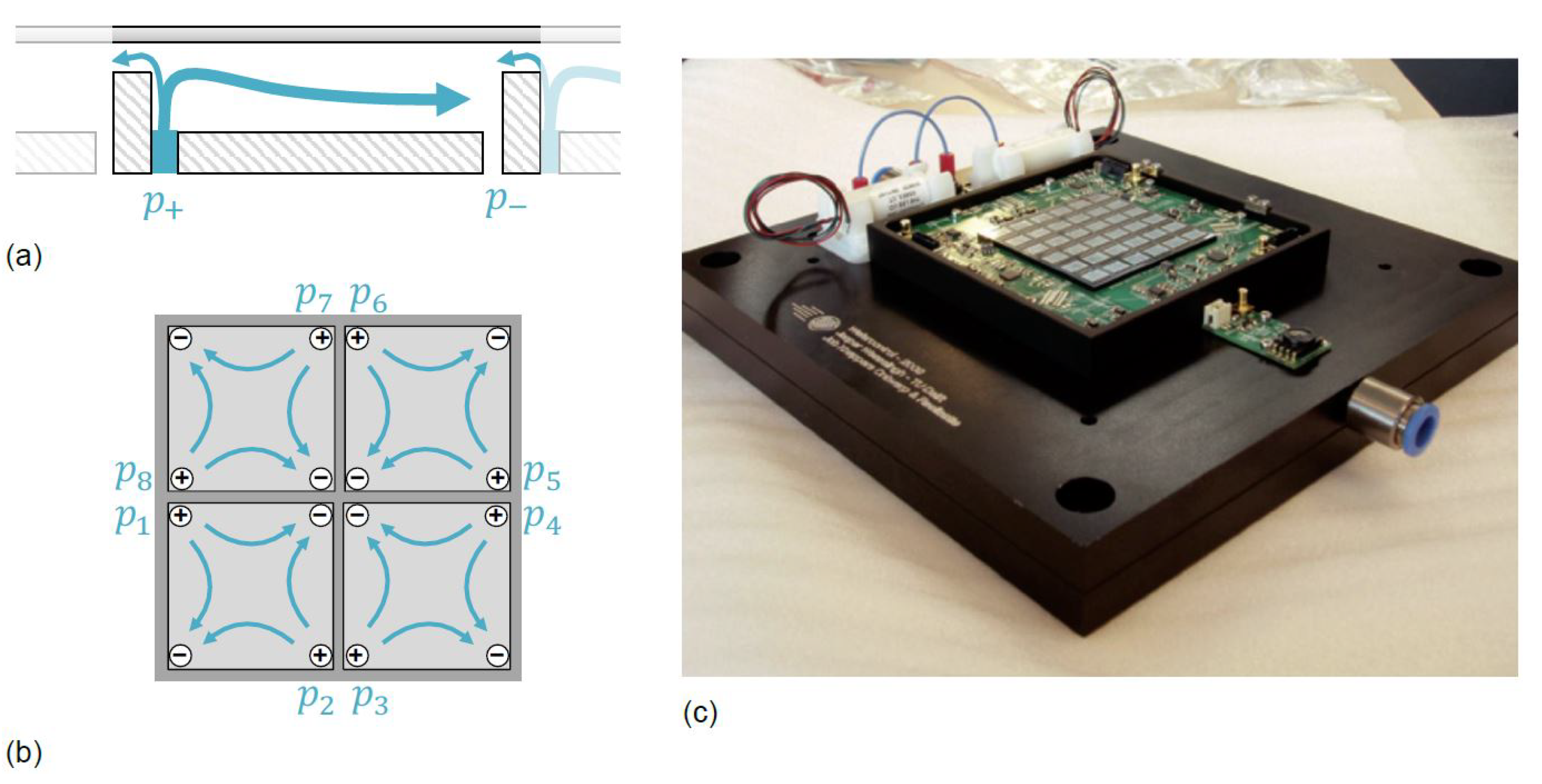
Figure 1a shows a cross-section of one of the actuator cells, where a substrate is floating on top of the pressurized air.
The air will flow from the inlet
p+ with high pressure to the outlet
p-, where the air is removed from the cell at a sub-ambient pressure. The viscous shear of the airflow creates a traction force on the substrate. The direction of the flow within a cell is controlled by changing the pressure at the different inlets. Four actuator cells have to work together to actuate the substrate in three degrees of freedom. The flow of the different cells is separated by dams. Four actuator cells are shown in
Figure 1b.
The final system was used to position a 4-inch silicon wafer, a demonstrator as shown in
Figure 1c. A bandwidth of
was realized using a PID controller. The system had a maximum acceleration of
, with an error of
, while using an external active vibration isolation system. The concept’s performance was limited by the manufacturing tolerances of the system, since this placed a lower limit on the fly height of
. A lower fly height would result in a higher actuation force. The other limiting factor was the time delay caused by the pressure lines between the control valve and the pressure inlet in the cell.
2.2. Variable Outlet Restriction
In 2017, Verbruggen designed the third generation of the contactless actuator which uses an outlet restriction to create the traction force. The dams can be actuated to restrict the flow at one side, while the flow is opened up at the other side. The concept is similar to the variable inlet pressure design. The advantage of this system is that the restriction is close to the chamber. This is an improvement, because there is no delay present at the supply lines, which limited the variable inlet pressure stage.
A demonstrator was built to prove the concept. Seven circular pockets have been produced. The substrate was controlled in open-loop. Using feedforward average angular accelerations have been measured of .
2.3. Transportation
Besides positioning a substrate on a stage, this technology can also be used for transportation thus further reducing the need for mechanical contact in a typical production system. In 2016, Vagher investigated the construction of a passive contactless conveyor [
6]. In this research, a cost-effective manufacturing technique for the passive conveyor surface was explored.
Vagher’s conveyor concept moves substrates in 2D and measured the position of the substrate using an automated vision system. The vision system resulted in a resolution of
at
. In continuation, Snieder investigated the transition between active and passive surfaces, which makes the transportation concept more versatile [
7].
2.4. Deformable Surface
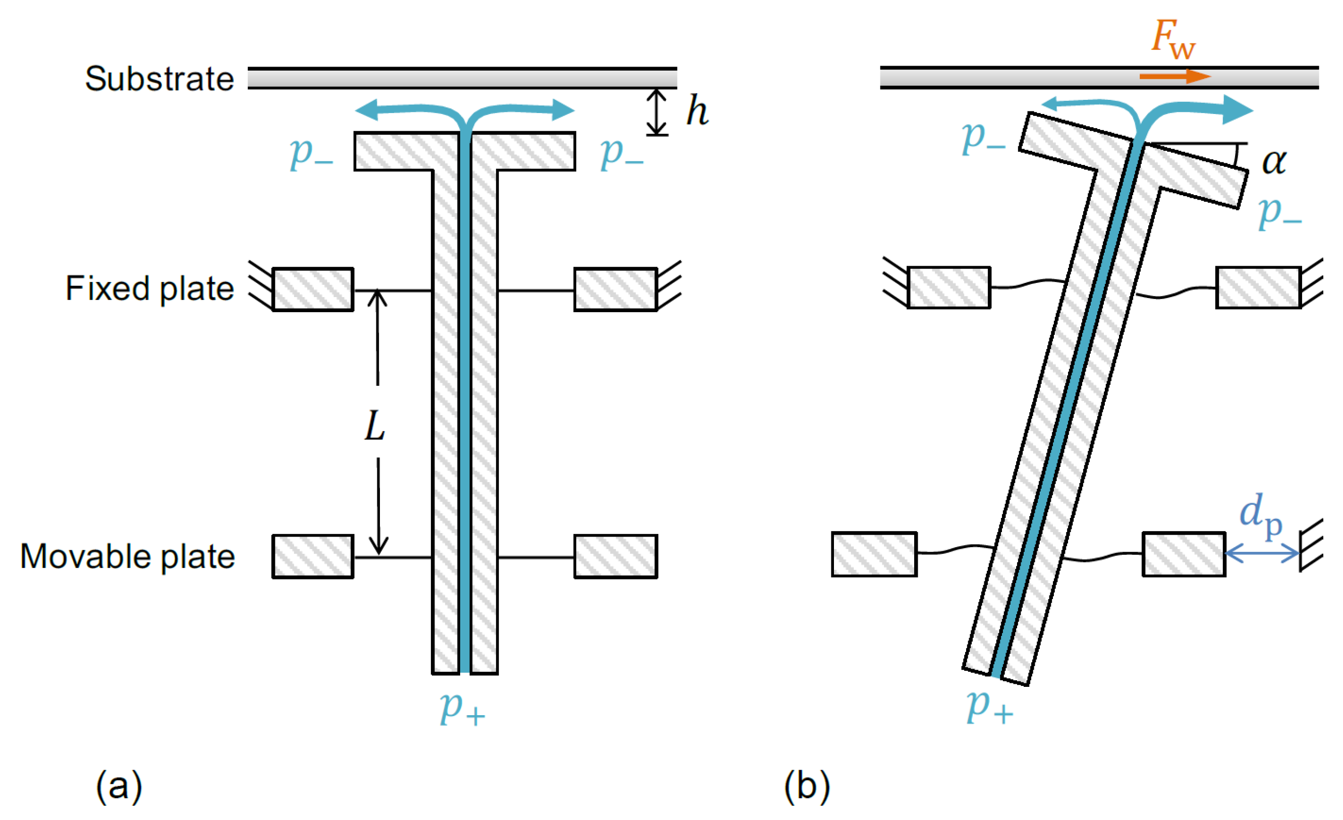
In 2011, Vuong explored a new concept regarding contactless positioning, “Air-based contactless actuation system for thin substrates” [
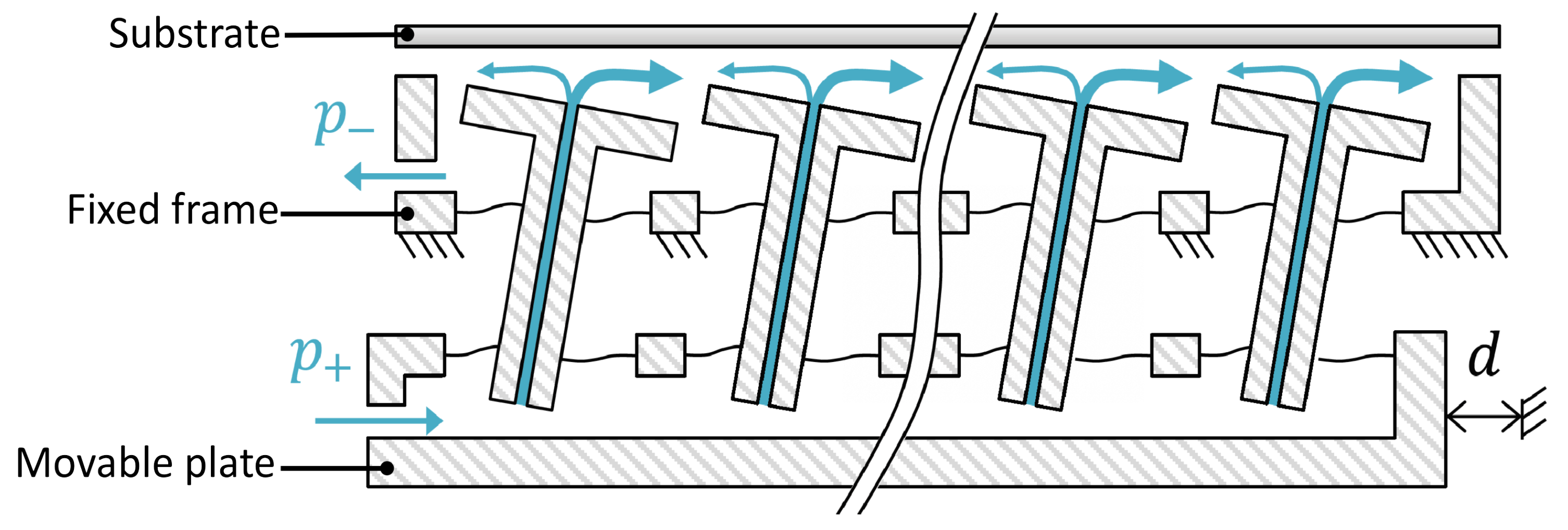
4]. The concept is based on multiple tilted surfaces to steer the airflow, and therefore the force on the substrate. The advantage of the tilting surface is that a change in the geometry directly generates a change of the shear force on the substrate. This concept does not suffer from the delay between the controlling action and force as seen in the first generation. In this concept, the in- and outlet pressure can be kept constant. The concept where the surfaces are tilted by bending the shafts is shown in
Figure 2. This concept is used in this paper for the precision contactless positioning of the wafer and is explained in detail in the next section.
3. Flowerbed
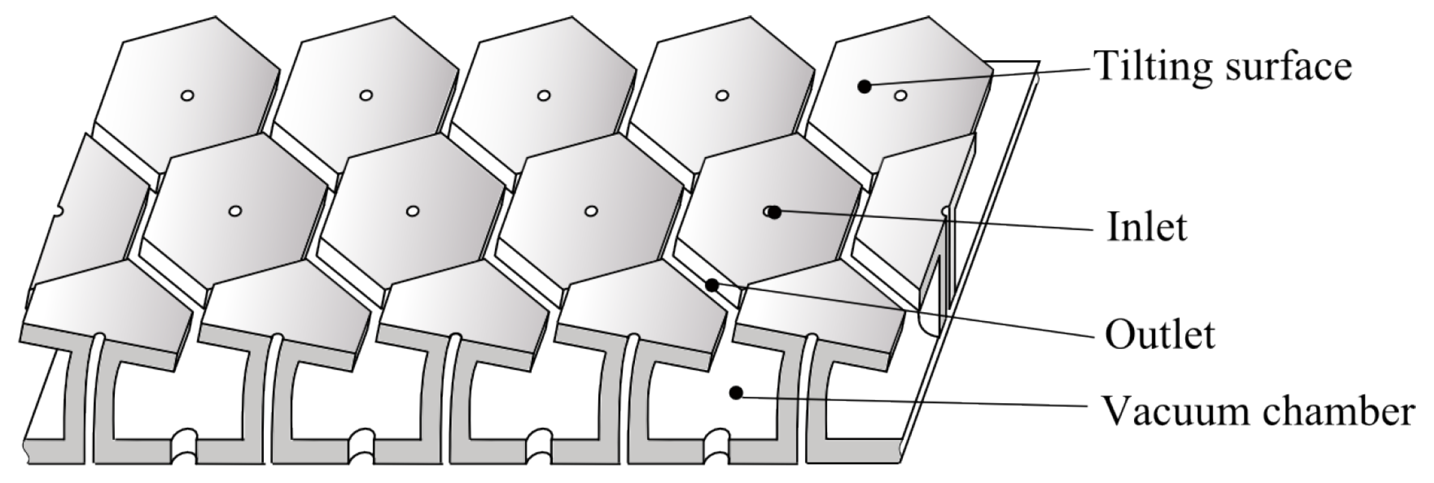
A demonstrator was built based on the bendable shaft concept. However, instead of bendable shafts, two membranes are used which allows the shafts to tilt. This reduces the force requirement of the actuator. The concept is shown in
Figure 3. The top membrane connects the flowers to the world. The bottom membrane is attached to the movable plate, which is connected to an actuator. The top membrane also functions as a seal for the upper chamber, which is connected to the vacuum pressure outlet. The inlet pressure comes in through the hollow centres of the shafts.
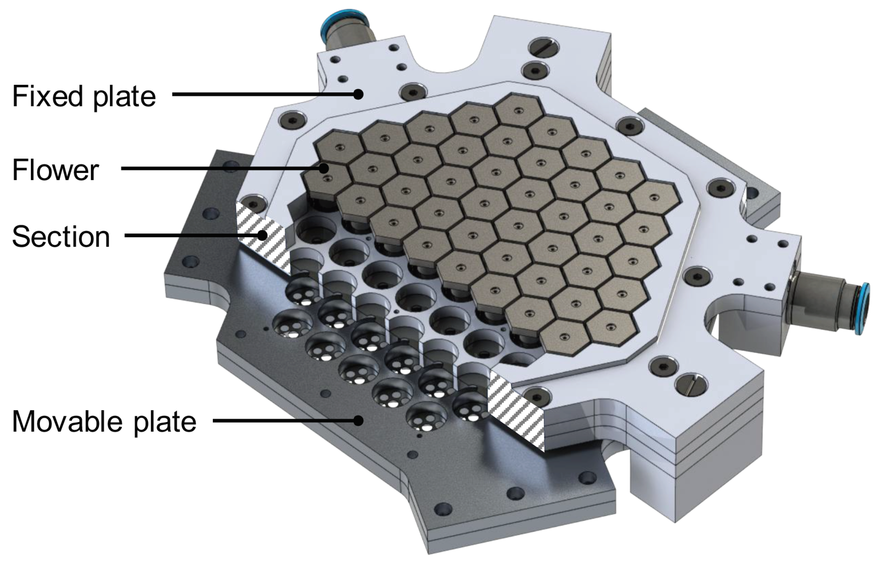
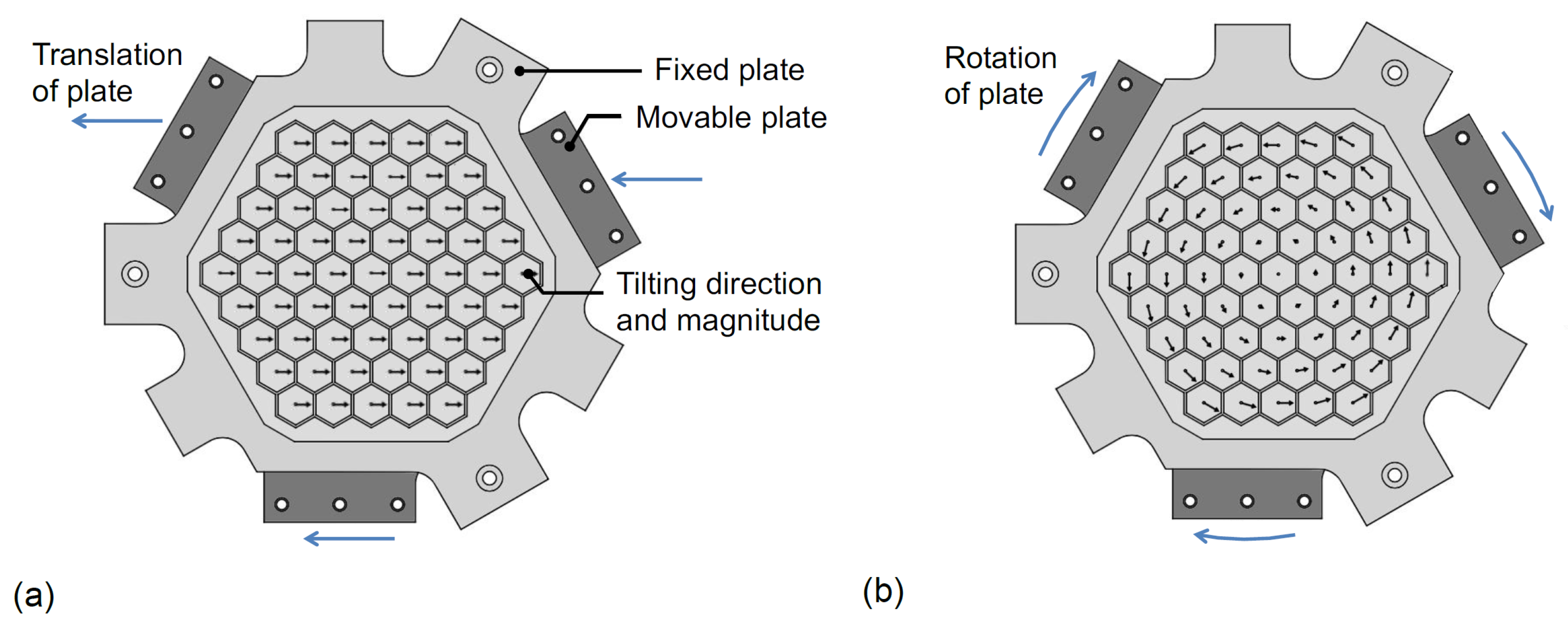
Figure 4 shows a cut-through view of the Flowerbed. The Flowerbed has 61 hexagonal heads, with an in-radius of
. It is nicknamed the Flowerbed because the surface looks like flowers that tilt towards the sun. The hexagon shape of the flowers was selected because it provides a full packing of the surface in combination with an optimal circumference to surface area ratio, and thus a maximum force for a given airflow. Furthermore, the figure also shows the fixed plate and movable plate, where both consist of two plates that are clamped together with a
thick membrane in between. The membrane is also clamped in the flowers. To better align the flowers, the movable plate is preloaded downwards with three springs, with a force of approximately
. After assembly, the final step was the spark erosion of the surface with wire-cut EDM technology to further level the surface.
Figure 5 shows a single flower in both a neutral and actuated position. The thin film airflow is visualized in the area between the effective surface of the flower and the substrate. The combination of the positive and negative pressures provides stiffness in the out-of-plane direction at the fly-height
h.
The flowers are tilted with an angle
, through a displacement of the movable plate, as shown in Equation (1). Where
is the displacement of the movable plate and L is the distance between the movable plate and the fixed plate.
when tilted the majority of the airflow will follow the path of least resistance. This flow will, in turn, exert a viscous traction force
on the wafer in addition to the out of plane stiffness.
The tilting angle of the flower has been measured to be proportional to the displacement of the movable plate up to
, without delay. The tilt response between the individual flowers is similar, there is only a small deviation in the gain. The values of gain vary between
and
, where the predicted value is
[
4]. Furthermore, Vuong experimentally validated that the pneumatics can be modelled by a proportional gain, up to at least
. This means that if the movable plate position is known, the force exerted on the wafer is known.
The stiffness of the Flowerbed is different for the translation and rotation of the movable plate. Each flower has an elastic hinge at the top and bottom, which provide stiffness against rotation.
Figure 6, shows the behaviour of the Flowerbed during the translation and rotation of the movable plate. The stiffness and inertia values for translation and rotation result in two suspension eigenvalues. These values have been calculated and experimentally validated by Jansen [
13]. The important properties are summarized in
Table 1.
Flowerbed Actuation
In 2016, Krijnen designed a reluctance actuator to actuate the movable plate of the Flowerbed [
14,
15]. Reluctance actuators can provide a high force, but they also have a high mass. With the use of fractional order control, this resulted in a control bandwidth for the Flowerbed of
. The bandwidth was limited by the eigenmodes caused by the actuator as shown in
Figure 7.
Figure 8 shows the flapping mode of the actuators that was limiting the bandwidth. The position of the wafer is measured using optical sensors. This required that gratings are attached to the wafer. The position of the wafer is controlled with a bandwidth of
.
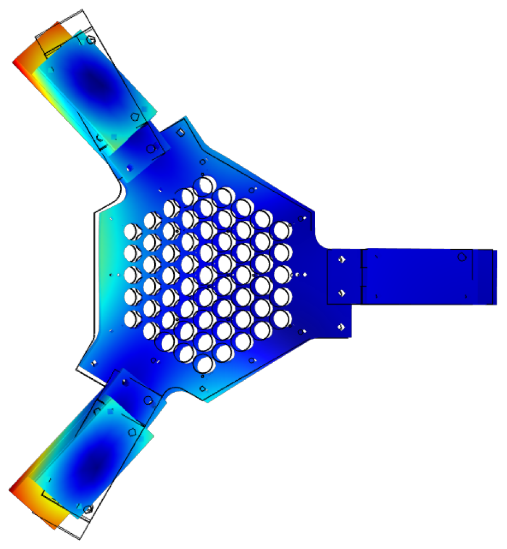
To increase the bandwidth of the system, Jansen redesigned the actuator in 2018. The new actuator was designed with special care for dynamic performance. Instead of traditional hinges, a design with notch flexures is chosen. The flexures provide a high stiffness in the out of the plane direction and work without backlash. The reluctance actuators have been replaced with Lorentz actuators, because they have a linear force current relation. Furthermore, the permanent magnets were placed on the stationary frame, and the coils on the mover, resulting in a minimal moving mass.
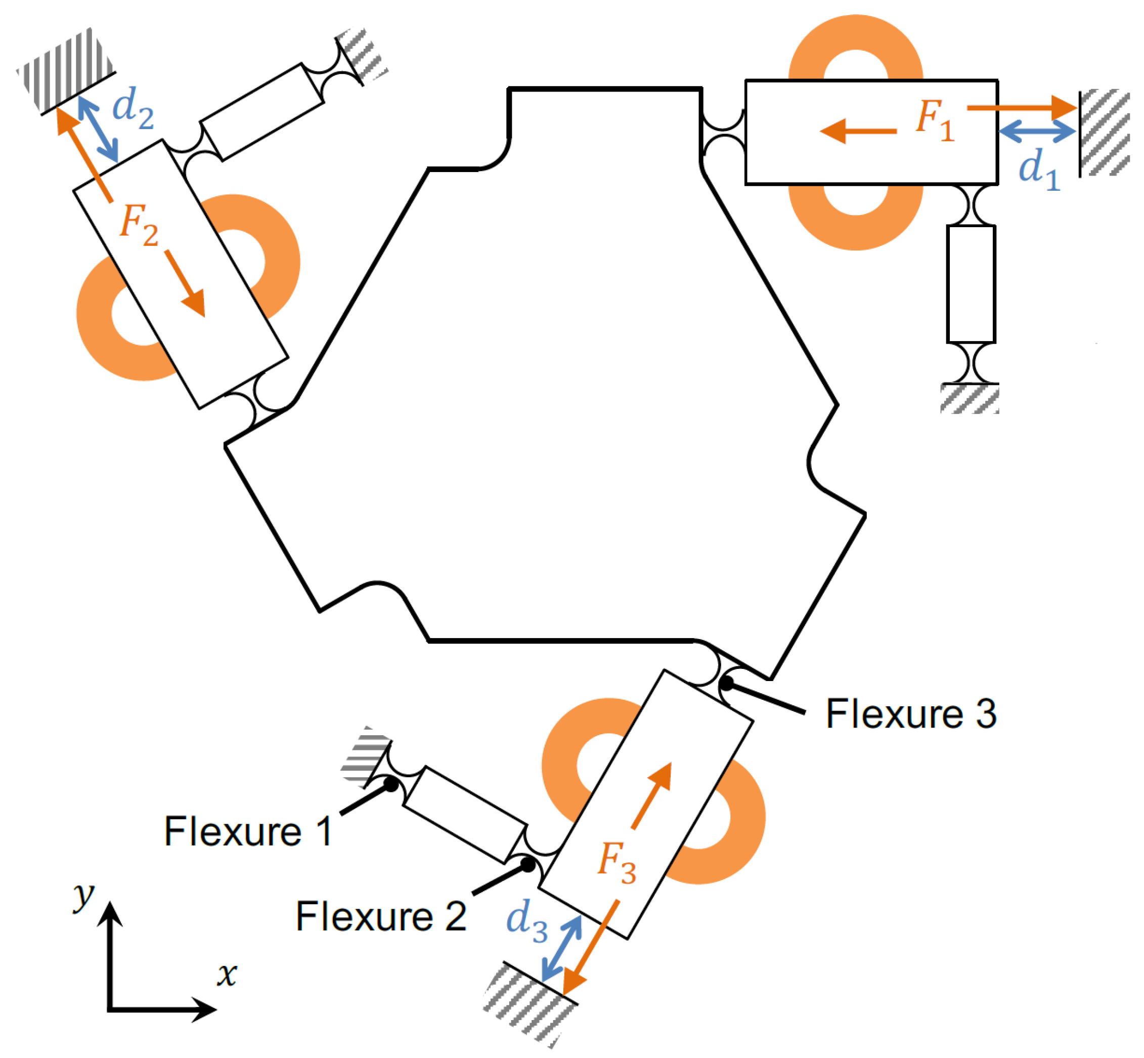
Figure 9 shows the chosen guidance for the movable plate. In the figure, the application point of the force and sensor are shown, as well as the notch flexure and guide linkages. The sensors that measure the actuator displacement are placed close to the actuator.
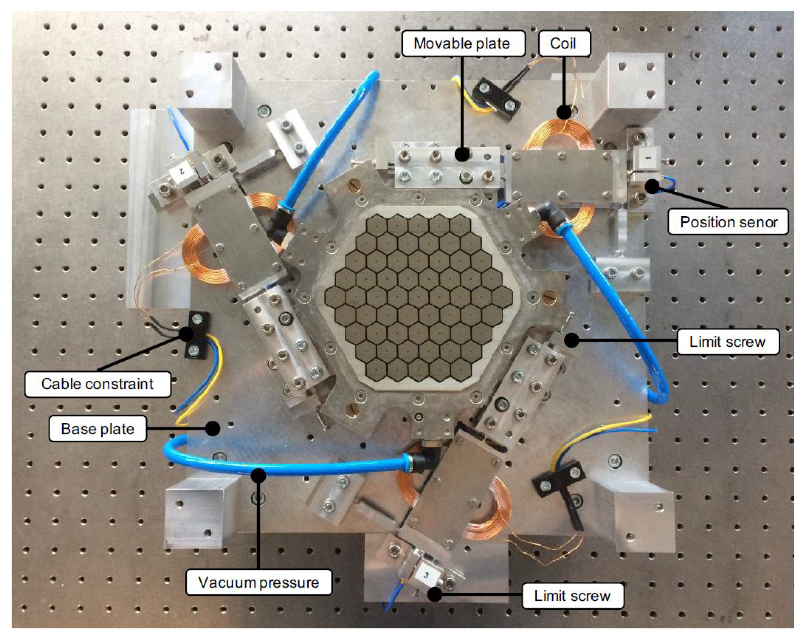
Figure 10 shows the Flowerbed including the realized actuator. From top to bottom it shows the connection between the actuator and movable plate. The coil is used to generate the force on the movable plate. The sensor is placed directly behind the actuator. The actuators have a relatively small motion range thus the wires running from the coil to the base plane are no problem. Furthermore, the stiffness is small compared to the stiffness of the movable plate [
13].
The position of the actuators is measured using Micro-Epsilon CapaNCDT CS08 capacitive sensors, which have a range of . With the 16 bits ADC this resulted in a resolution of . The noise is measured at peak-to-peak, with an RMS value of .
4. Flowerbed Dynamics and Control
In the previous sections, the state of the art has been presented. The bandwidth of the compliant actuator design was placed on . No sensor was implemented to measure the position of the wafer. In this section, the dynamic response of the system is presented. A controller is designed and the closed-loop results are discussed. At last, the possibilities for improvement are discussed.
4.1. Flowerbed Dynamics
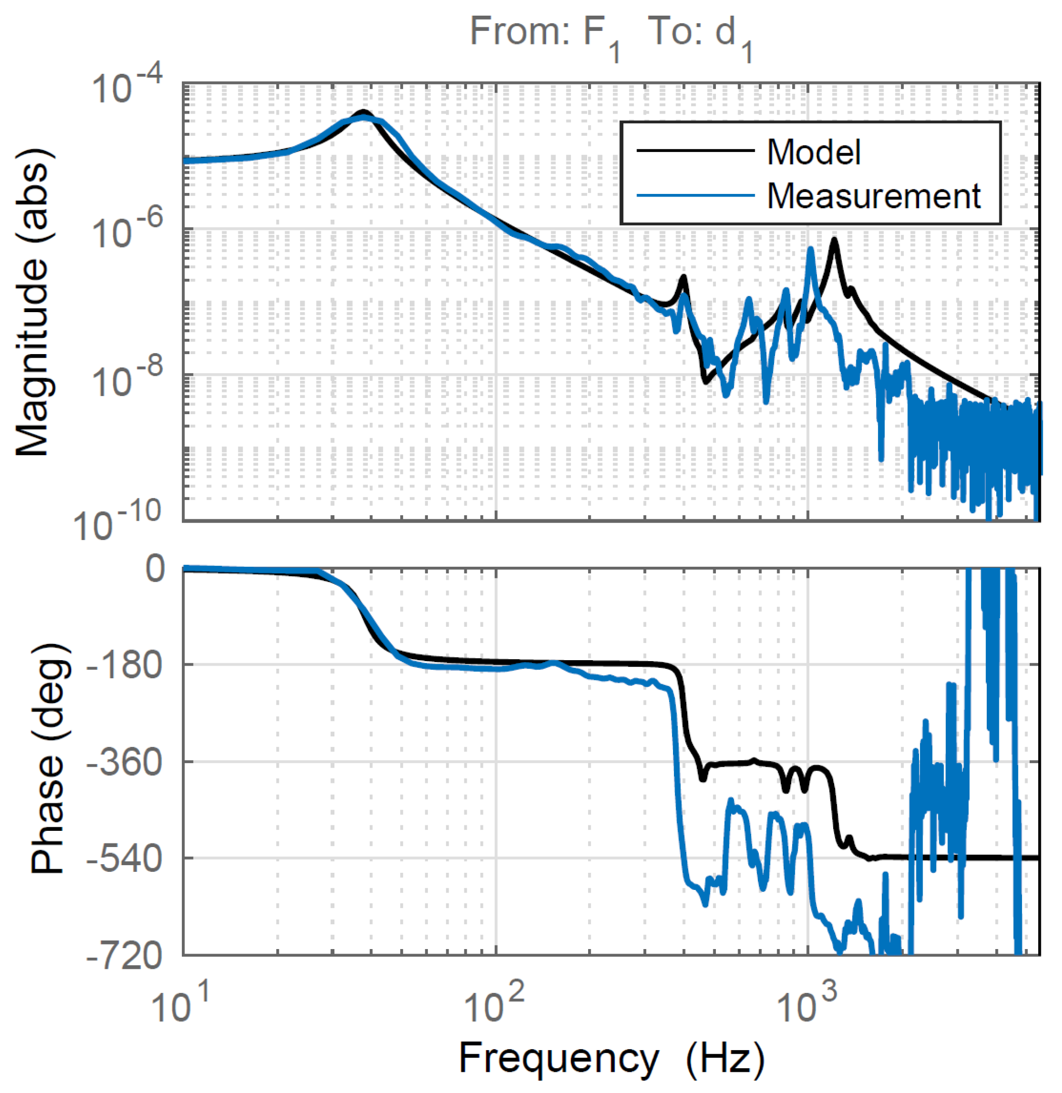
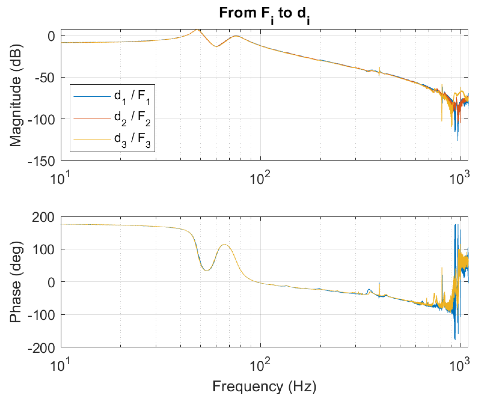
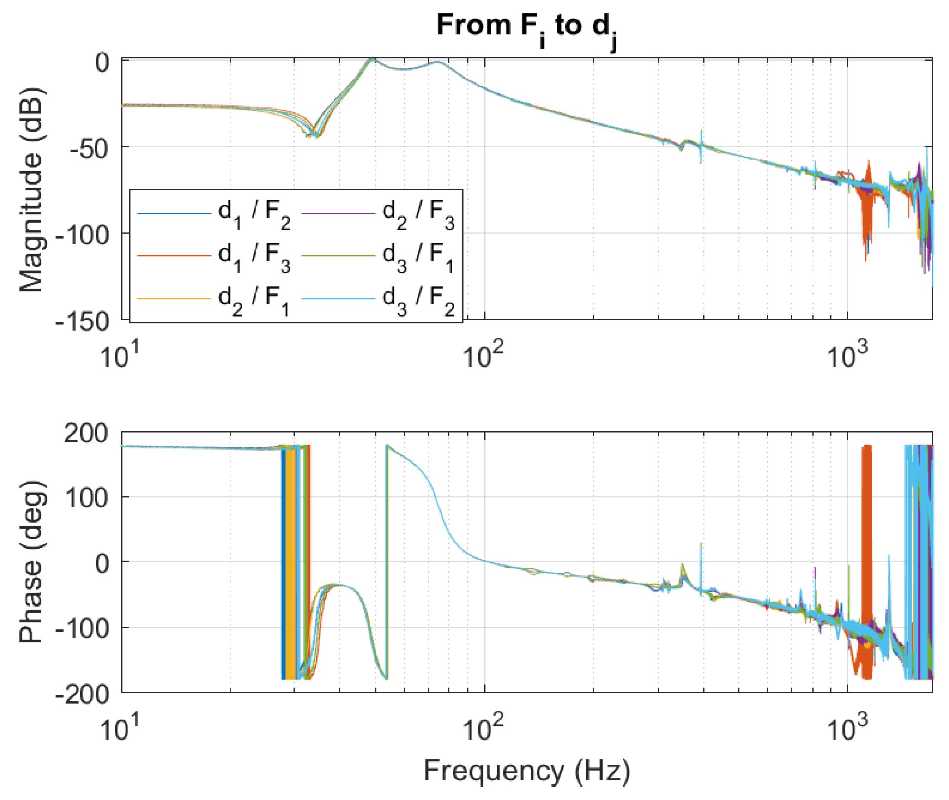
Figure 11 and
Figure 12 show the results from the identification where all the straight transfers and cross transfers are plotted. The directions of force and position sensor are inverted and account for the 180
phase seen. Both transfers show a quick drop in phase which is the limiting factor for the bandwidth. Jansen suggested this could be the effect of the capacitive sensing system [
13]. This large phase drop was investigated as part of this work. After investigation of the delay sources in the system— amplifier, capacitive sensors, sampling time, and coil dynamics—the main sources of the delay have been identified. The phase lag is due to a combination of the
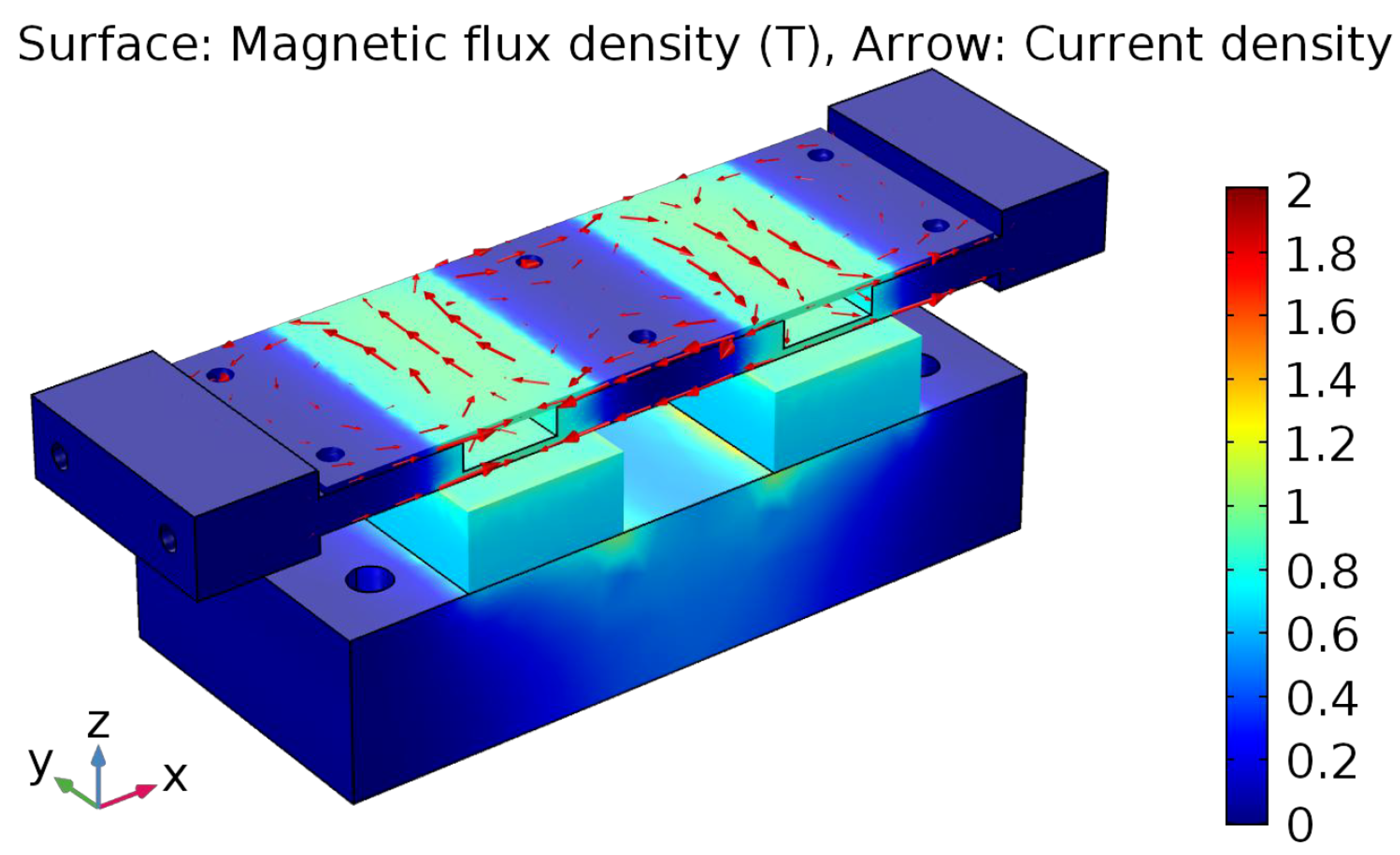
sampling which produces a phase lag and the magnetic field which is lagging the current. The lagging field is due to the eddy currents in the mover which will create a magnetic field opposing the movement. When the magnetic field of the coil and eddy current are summed the field lags that of the coil alone. This provides a time delay seen in the bode diagram as a lagging phase. Furthermore, the eddy current damping provides damping of magnitude proportional to the velocity of the mover.
Figure 13 shows the mover in the magnetic field of the permanent magnets. The mover consists of an aluminium plate with spaces cut out for the coils and a top plate to hold them in place. A solution to limit the intensity of the generated eddy currents is to laminate the mover. Another method is to look at the possibility of flux feedback for the amplifier of the system, to compensate for the effects of the eddy current [
16]. These solutions have not been implemented in this work and are left for future work.
4.2. Flowerbed Control
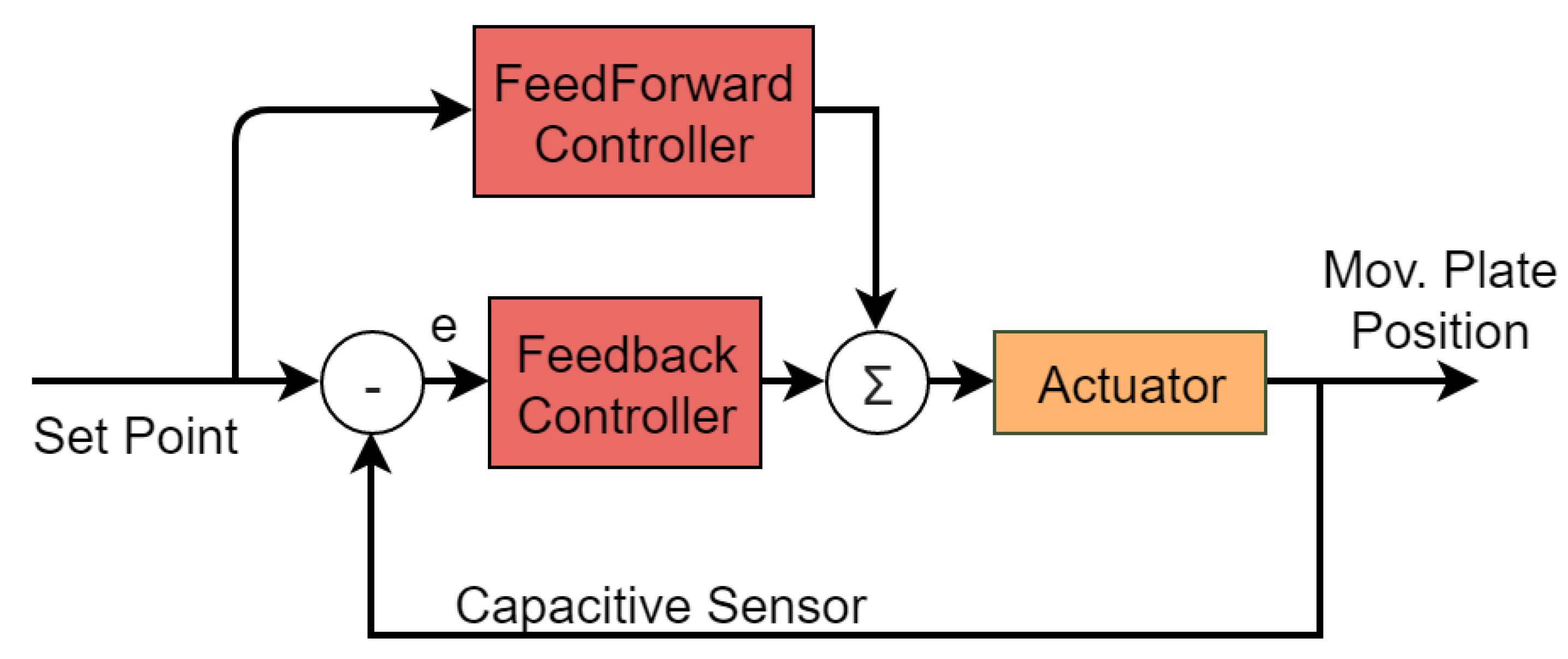
The controller of the inner loop will control the position of the actuator to the corresponding sensor. The measured position will be controlled using a feedforward controller and feedback controller. The diagram is shown in
Figure 14.
For the feedback controller, a PID controller is designed for a bandwidth of
. The parameters are shown in
Table 2, the gain for actuator 2 is different to compensate for the slightly different stiffness at the bandwidth. The controller creates a phase margin of 27
, gain margin of
, and a modulus margin of
.
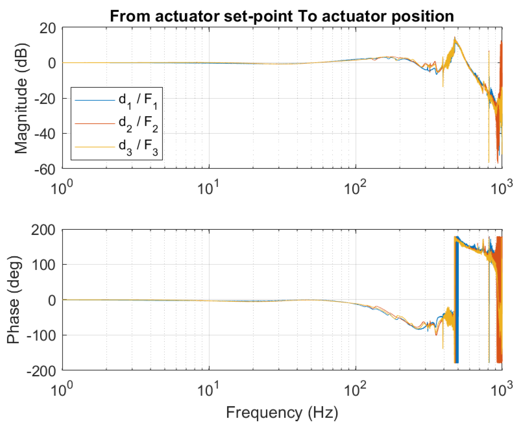
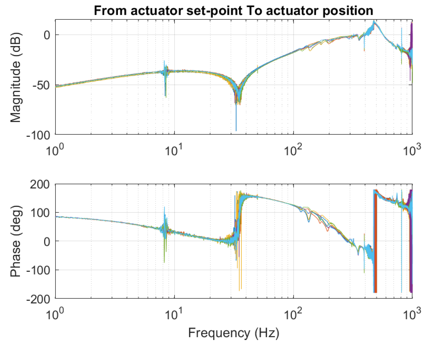
The feedforward controller has been designed using a simplification of the plant. The feedforward controller is the inverse of this plant made proper with two second-order low pass filters at the frequency of the bandwidth. The closed-loop response of the system with the PID controller and feedforward is shown in
Figure 15 and
Figure 16. The feedforward controller is given in Equation (2).
The closed-loop response of the system is similar for all three actuators. The response provides a good basis for the outer loop controller up to, at least . The system shows strong coupling at , this could be improved using a decoupling filter or by prefiltering the input. Because the bandwidth of the outer loop is limited, it is chosen to use the outer loop controller to prefilter the reference signal.
5. Wafer Sensing
The wafer floating on air is a floating mass with a viscous damping system, thus to gain control over the position of the wafer it is necessary to have a collocated sensor. For this sensor in the outer loop, there are some restrictions, that influence the sensor choice. For the high-tech industry, it is unappealing to use a wafer modified to accommodate the sensing solution. Thus, it is preferred that the wafer is not altered.
As discussed in the state of the art, different sensor techniques have been used in the past, such as techniques based on capacitive sensors, edge detection using charge-coupled devices (CCD), and vision and optical encoders. The best speed and resolution was achieved using optical encoders with gratings on the wafer. However, this is an alteration to the wafer. Without altering the wafer edge detection using the linear CCD sensor array is the best choice. Edge detection can reach sampling speeds up to multiple while having a sub-micrometre resolution that can be achieved using sub-pixel interpolation. This will be discussed later in this section.
5.1. Linear Sensor Array
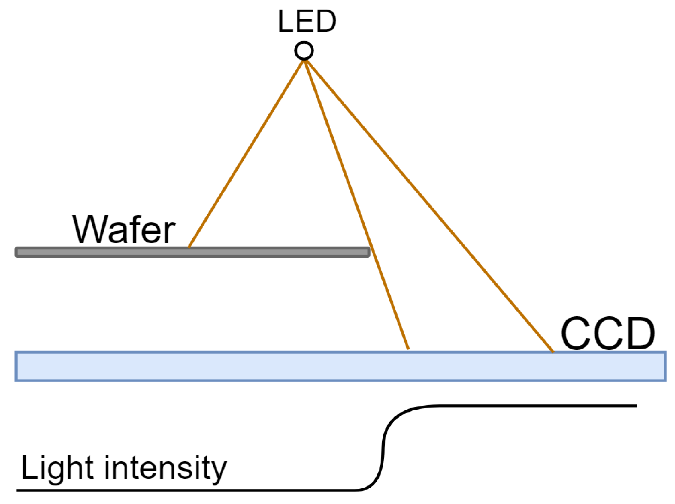
A linear CCD has been selected to measure the edge position of the wafer. It consists of an array of pixels that measure the intensity of the light. The change from light to dark is used to find the edge of the wafer. The concept is shown in
Figure 17. As discussed in the state of the art, Wesselingh had implemented CCD sensors but used a somewhat different concept where noise from stray light limited the performance [
3].
The selection of the CCD sensor is based on a trade-off between the resolution, sampling time, and range. The sampling time is limited by the available modules for the National Instruments CompactRio. The NI9201 is used which supports . The TCD1103GFG has 1500 pixels of by on a center. It supports a data rate of . With 1500 pixels and a low integration time this results in a sampling rate of almost , and with the limitation of the this is lowered to . High power cool white LEDs are used as the light source. The intensity of the light is tuned to maximize the dynamic range.
In this paper, the sensor output is compared to a threshold. This threshold is used to detect the transition from light to dark. Instead, a threshold a sub-pixel interpolation method could also be used. Using this method it is possible to increase the resolution of the sensors to better than 0.05 of the pixel size, while at the same time reducing the effects of noise [
17,
18,
19,
20]. Using the sub-pixel interpolation method the theoretic resolution of the chosen CCD could be as low as
. However, to limit the calculation time on the FPGA, it was chosen to implement the threshold model.
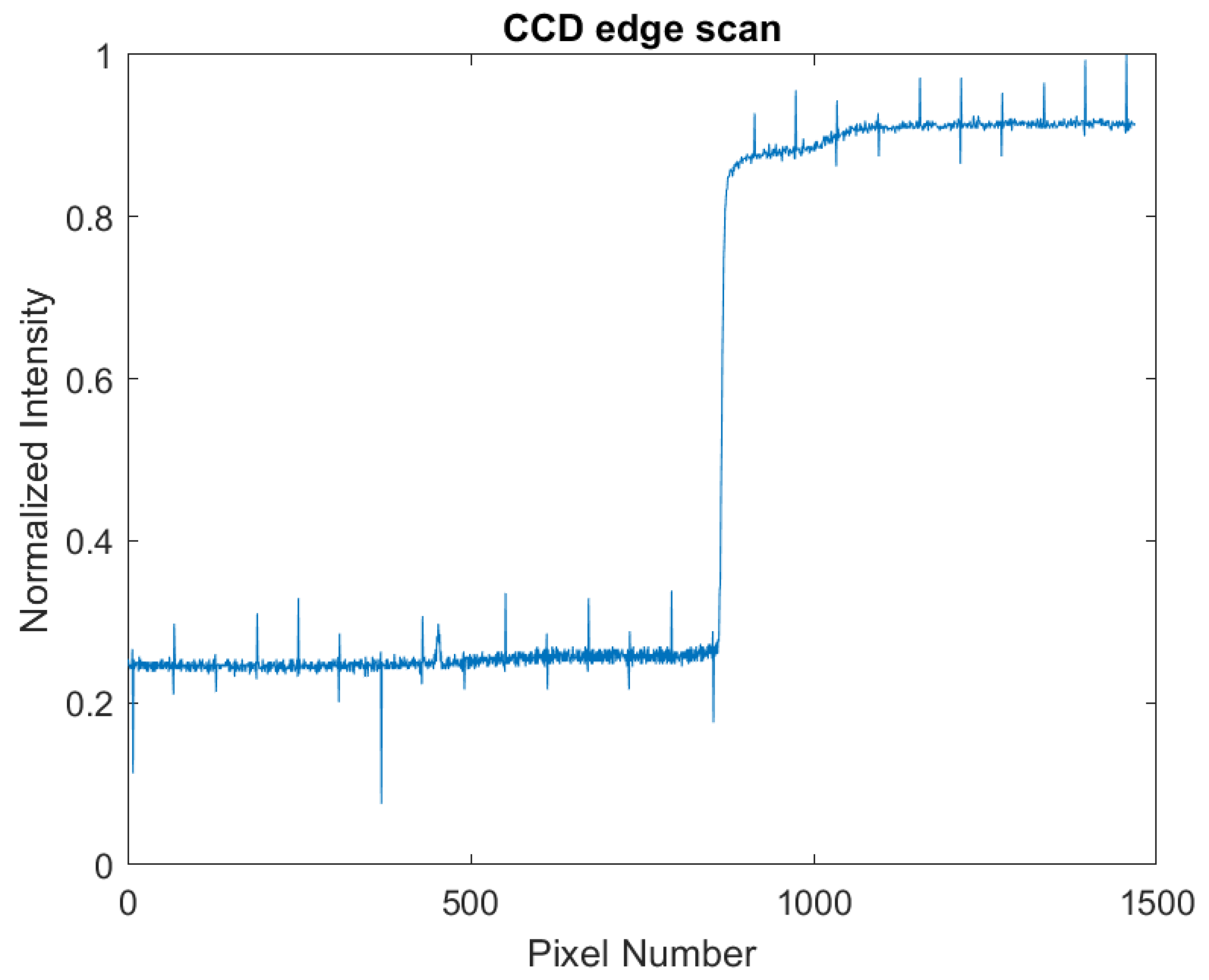
Figure 18 shows the output of the CCD sensor. The threshold is placed at 0.6. When the threshold is reached the pixel number corresponds to the position on the CCD where the shadow ends.
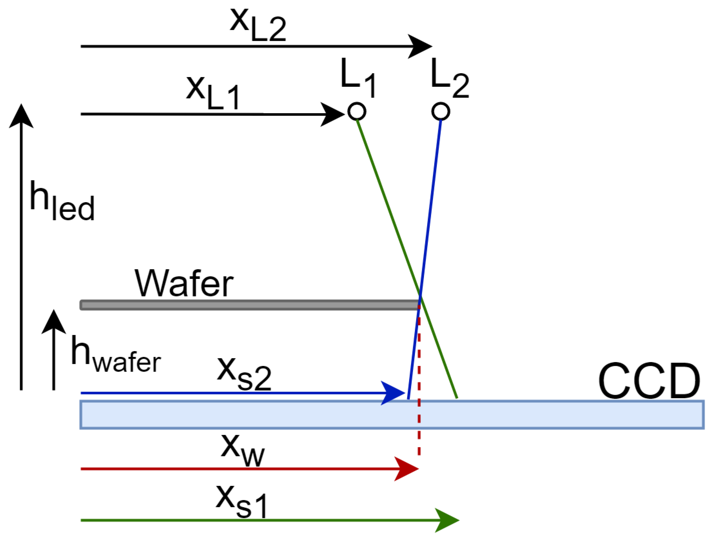
When using a point light source, the measured position should be adjusted to get the real position.
Figure 19 shows that the distance between the shadow and the wafer position is dependent on the position and height of the wafer. The wafer position is calculated using Equation (3a). Because the height of the wafer is not fixed a disturbance could enter the system through a variation in the height. The size of the disturbance can be estimated by Equation (3a).
The difference in fly-height is estimated to be in the order of micrometers. When minimizing the height between the wafer and CCD the disturbance is estimated to be within 0.1 of the pixel size for large movements, which is acceptable when using the threshold model, if sub-pixel interpolation is used it is better to remove the height by using a collimated light source or by adding another LED. With two LEDs, another data point is known which can be used to eliminate the height from the equation as shown in Equation (3b) [
21].
5.2. Performance Analysis
Before the implementation of the CCD sensor inside the contactless actuator, a performance analysis experiment was done. In these tests, the linearity of the sensor was tested, as well as the steady-state behaviour. The performance test was performed in an environment where disturbance sources from the external lighting, vibrations, and the electrical side were not removed. The steady-state response shows no drift and high precision, since the position returns to the same position.
Figure 20 shows the performance analysis test where the position of the CCD is compared to a stage that has a resolution of
. The figure shows no drift and follows the position of the stage with an error of
RMS.
5.3. Metrology
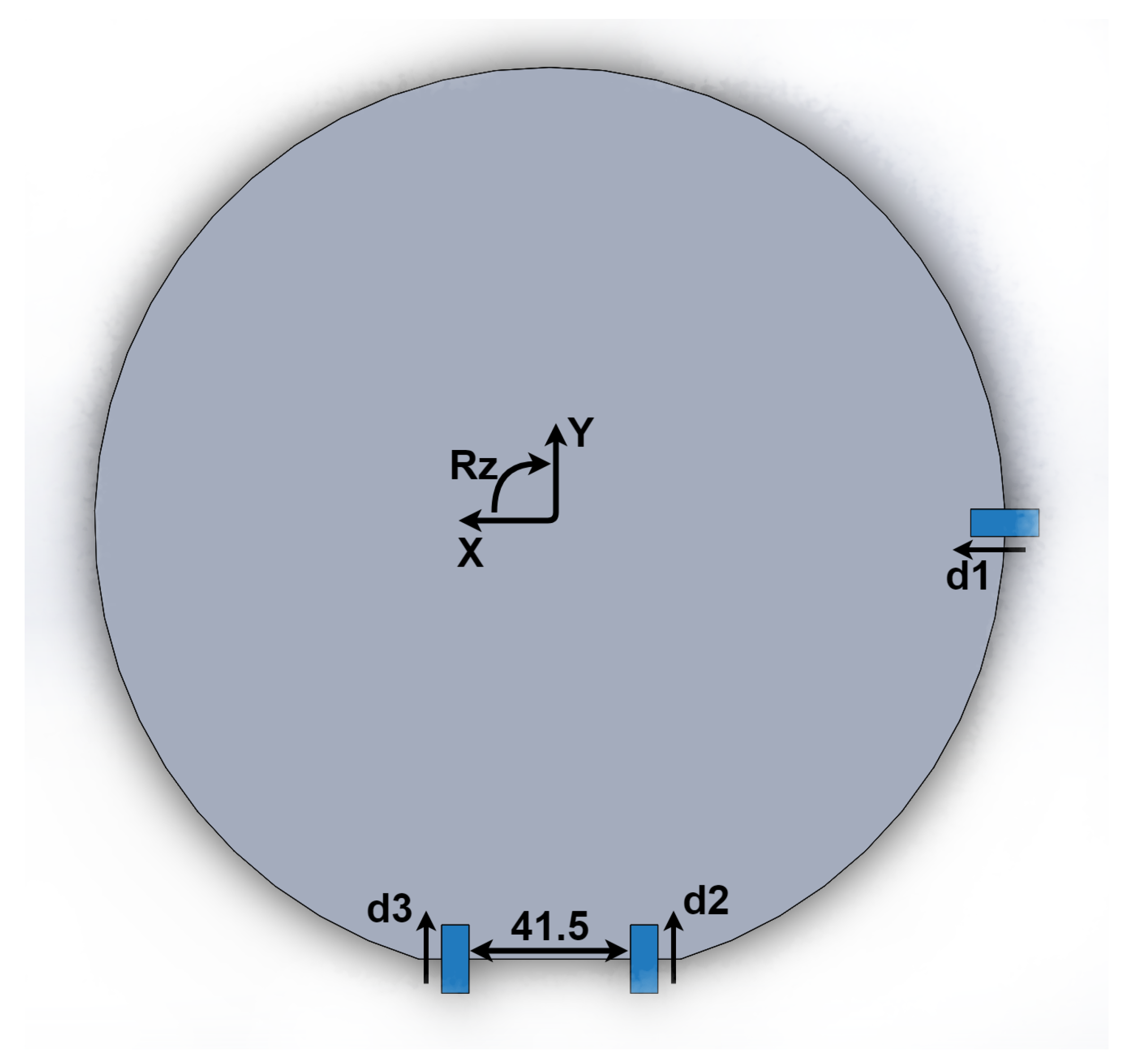
The kinematics are used to convert the measured position from the sensors into the position of the wafer.
Figure 21, shows the placement of the sensors. The kinematic equations are shown in Equation (4), where
r is the radius of the wafer and
the distance between the sensors. The input of the kinematic equations is in millimetres and the output is in millimetres and radians. The photograph of the Flowerbed system with the integrated contactless sensing is shown in
Figure 22.
The validation of the outer loop control was performed using a dummy wafer. The dummy wafer was cut out of a thick aluminium sheet according to the JEIDA standard. This means a circle with a radius of with a flat of . The aluminium wafer had a mass of , which is 8 percent more than a comparable silicon wafer.
6. Wafer Control
To control the position of the wafer, a second controller needs to be added to the inner loop Flowerbed control. This leads to a cascaded control structure as shown in
Figure 23. The Flowerbed controller will be called the inner loop controller (ILC) from now on. The ILC will provide a stiff connection between the Flowerbed and actuator. The setpoint of the ILC will be controlled by the wafer controller, which is also called the outer loop controller (OLC). The kinematics and inverse kinematics are placed in the loop of the OLC, because the OLC has a lower bandwidth and thus more time for the calculations.
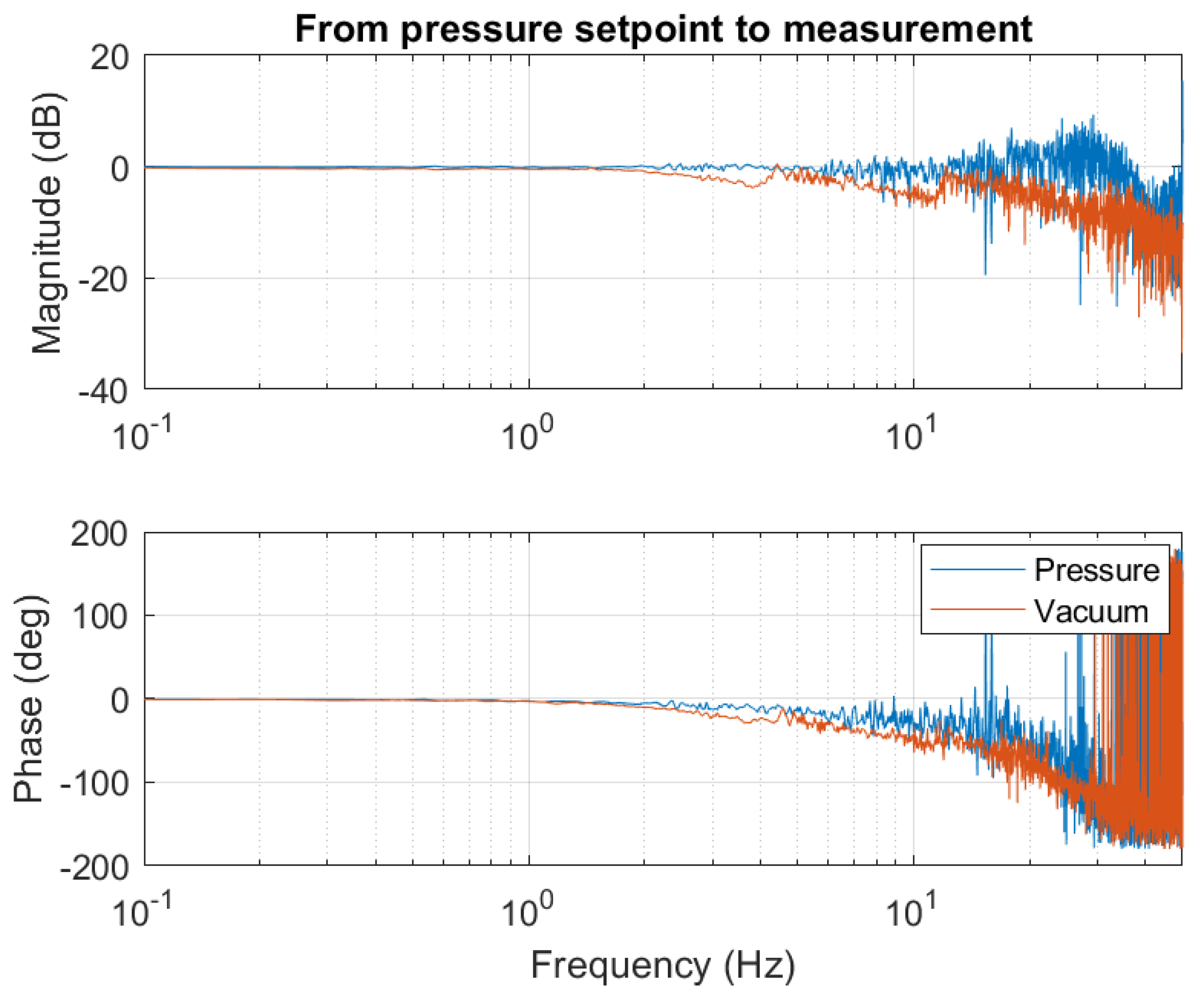
6.1. Pressure Control
For the operation of the Flowerbed, constant pressure and vacuum are crucial, even more so because of the non-uniform behaviour of the flowers on the surface for a given supply and vacuum pressure. As a result, setting a higher pressure will cause an extra force in the negative y-direction, whereas a lower vacuum will create an extra force in the positive y-direction.
To control the pressure, sensors and valves are placed in the supply lines. The dynamic behaviour of the pressure and vacuum supply has been identified around the operation pressure of
supply and
vacuum. The controller design is a proportional gain together with a second-order low pass filter with the values provided in
Table 3. The lower bandwidth has been chosen because of the limitations of the solenoid valves, increasing the bandwidth further does not improve the performance. The closed-loop frequency responses for the pressure controls are shown in
Figure 24. During control the steady-state error is measured, the error for the vacuum controller is
and for the pressure controller
.
6.2. Pneumatics
Previous experiments by Vuong showed that the air film dynamics can be described as a pure proportional gain up to at least
, after which the measurement became unreliable [
4]. The proportional gain of the system was determined at
. In short, this means that if the position of the movable plate is known, the viscous traction force on the wafer can be calculated up to at least
. This value of the proportional gain has been verified during the experiments of Krijnen [
14]. Furthermore, Krijnen provided the displacement force graph for different supply pressures while maintaining the vacuum supply at ambient pressure minus
.
Multiple experiments were done as part of this work with the values provided by Krijnen, however, the previously measured pneumatic gain could not be replicated again without mechanical contact. Multiple factors play a role here, the Flowerbed has been taken apart and reassembled multiple times to replace the actuators. Upon close inspection, it was noticed that multiple flowers were out of alignment. Furthermore, the supply pressure was leaking between the pressure sensor and the Flowerbed. This made the readings from the pressure sensor unreliable. The combination of these factors resulted in the fact that the noncontact criteria could not be guaranteed for a given pressure. Therefore, in this work, the pressure was manually tuned to obtain the best performance while maintaining the no-contact condition for a full movement of for the movable plate. The optimum was found at a vacuum pressure at minus and a supply pressure of . As a result, the value of the pneumatic gain was less than optimal and was approximated at .
6.3. Outer Loop Controller
In the outer loop, two separate controllers have been designed, one for controlling the rotation at lower bandwidth and one for positioning the wafer in x and y at a higher bandwidth to maximize the performance of the total system. The parameters of the controller will be discussed later in this section.
The outer loop could not be identified using the open-loop response because the system consists of a floating mass with viscous damping. The identification of the system could be done by adding stiffness to the mass or through simulation. The simulated open-loop transfer function could be described by the transmissibility of the inner loop controller (
), the pneumatic gain of the system and the wafer, which is a mass system. This is shown in Equation (5), where
is the outer loop controller.
For the controller, it is decided to use a PD controller with a low pass filter. The low pass filter must be placed before
to cancel out the coupling in the inner loop. Because of the high gain of the mass-line, it was chosen to leave out the integrator.
The gain of the system was calculated using Equation (6). The factor 4 accounts for the frequency range of the derivative part of the controller as given in
Table 4, which adds a gain of the same value. To start, the pneumatic gain
values calculated by Krijnen were used. This gives an initial place to start after which the controller has been tuned iteratively. After the initial measurement, the new controller gain could be calculated to compensate for the lower pneumatic gain.
6.4. Performance
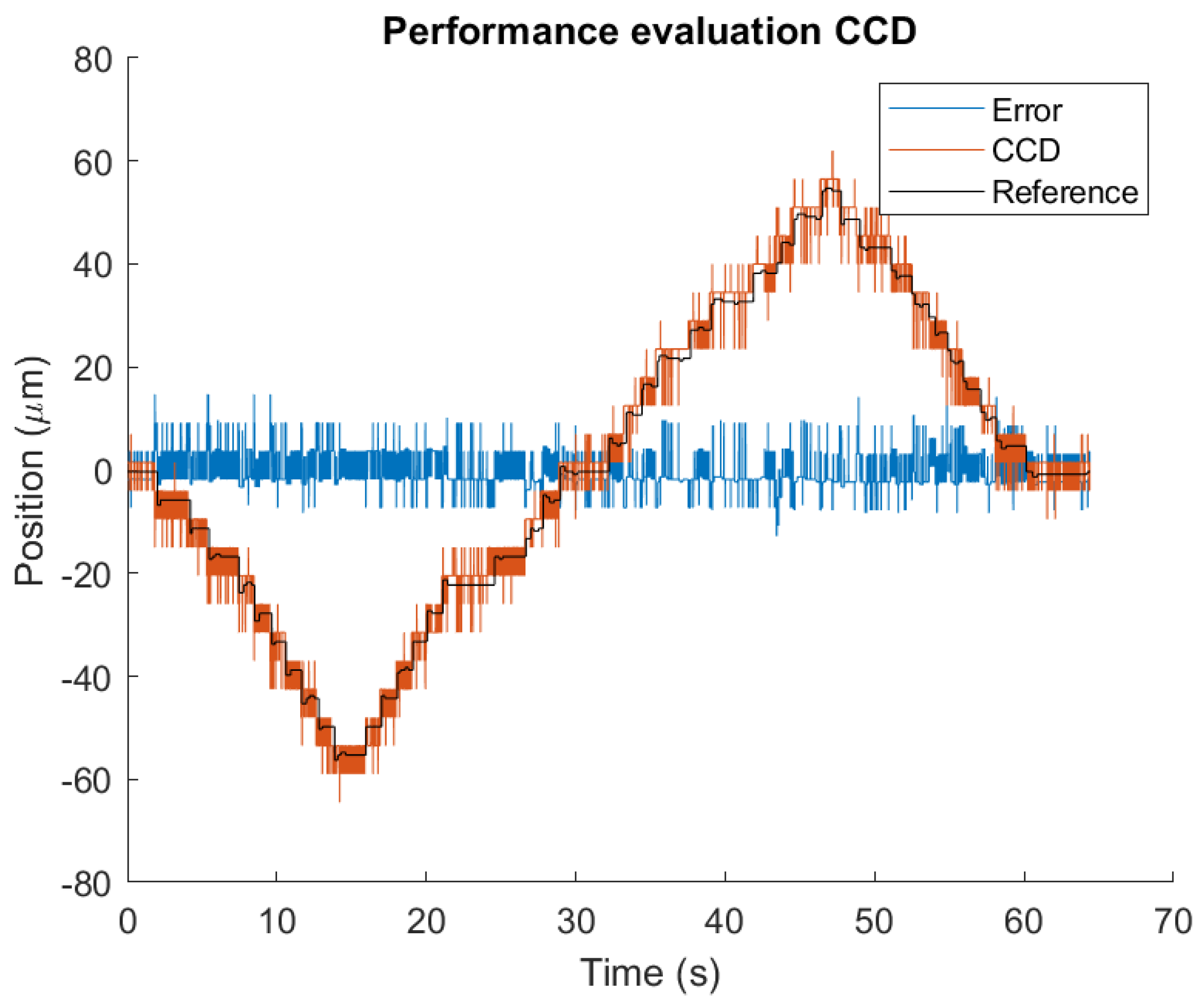
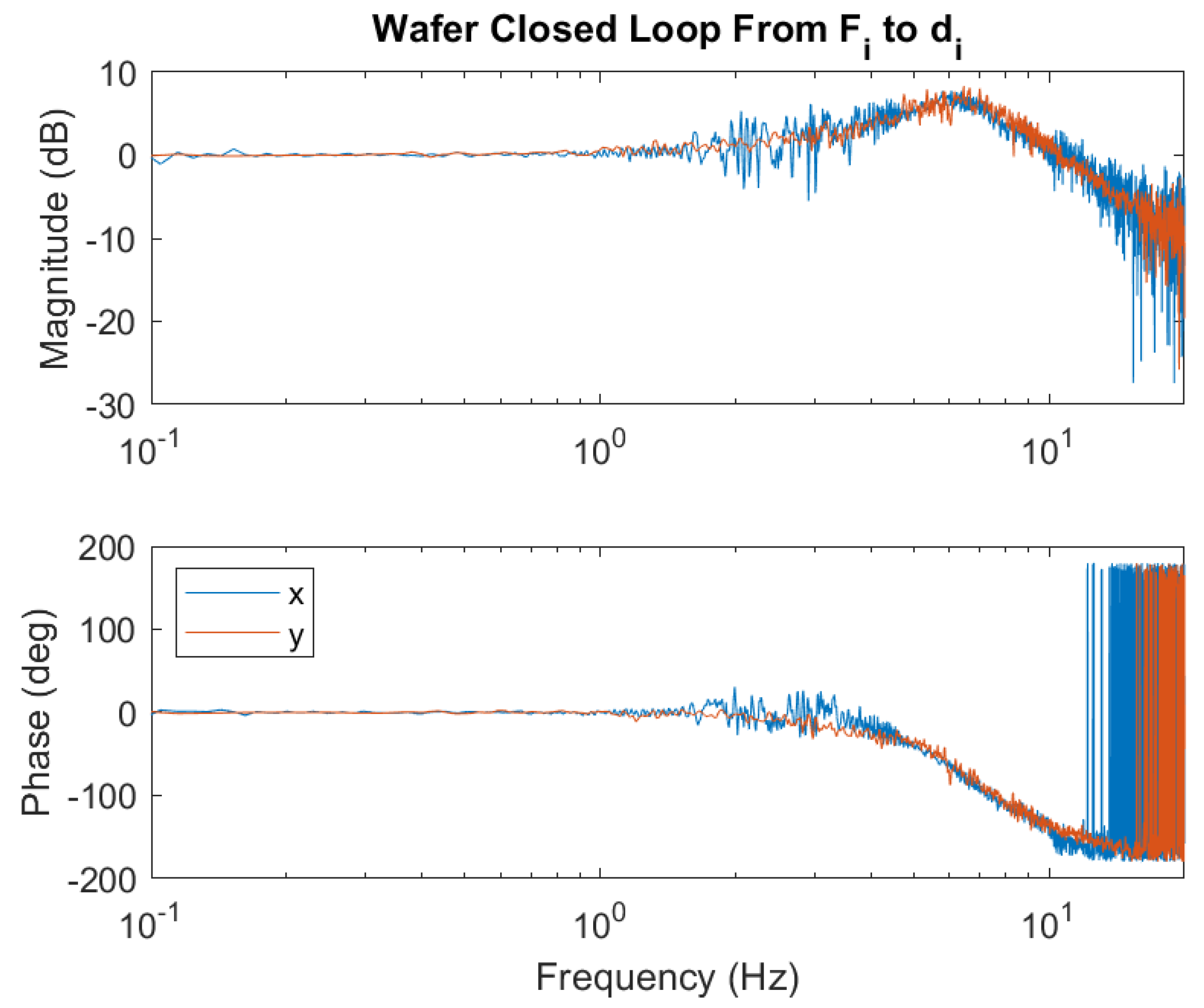
After tuning the controller for the inner loop, outer loop, and pressure, the performance of the positioning of the wafer has been measured.
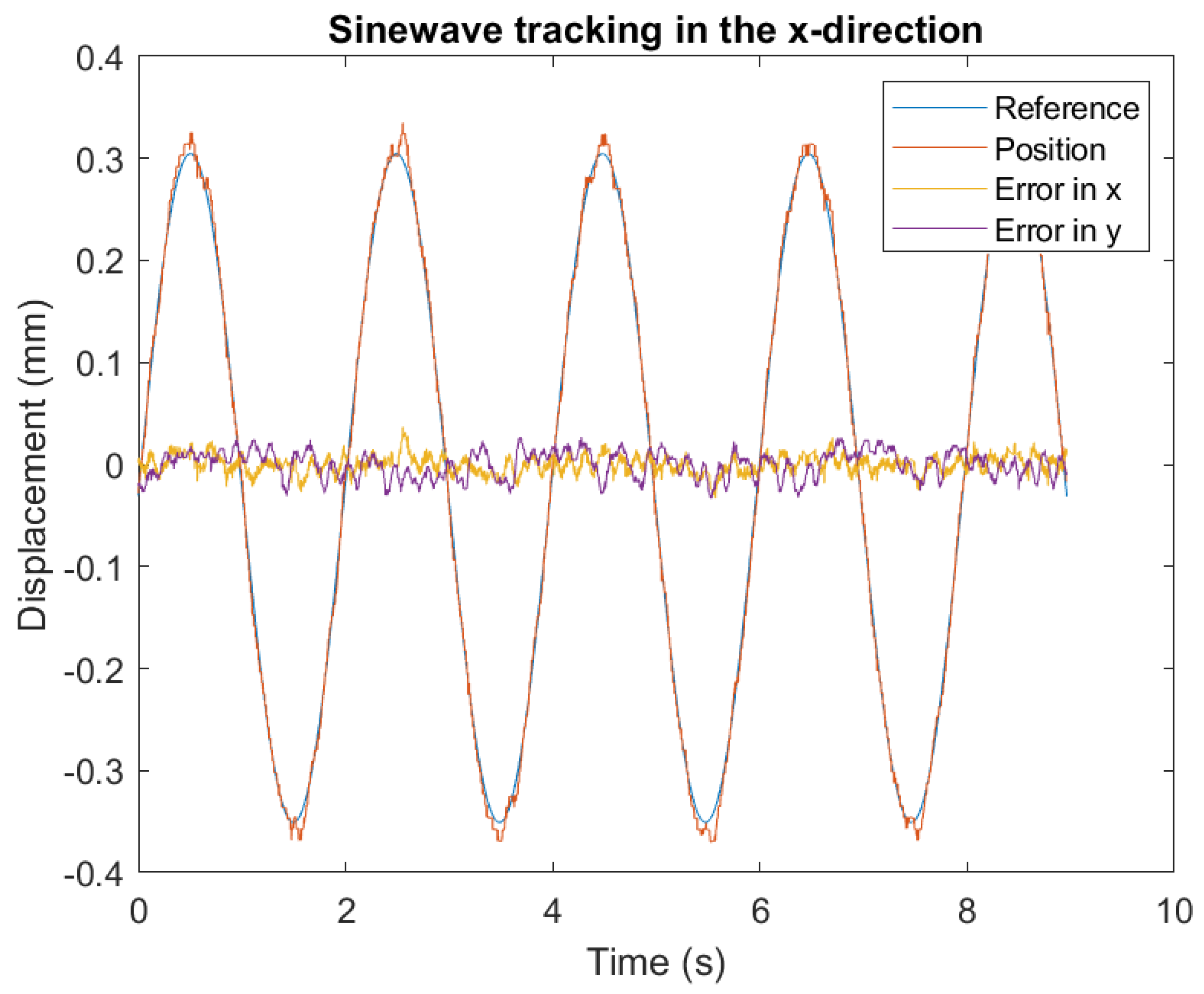
Figure 25, shows the closed-loop response of the system. The measurements for the cross-coupling between the x and y-axis are insignificant and thus not presented in the frequency domain. The error of the x and y-axis during tracking is presented in
Figure 26. Furthermore, when tracking a sine wave with an amplitude of
at
, the RMS error of x and y remained under
.
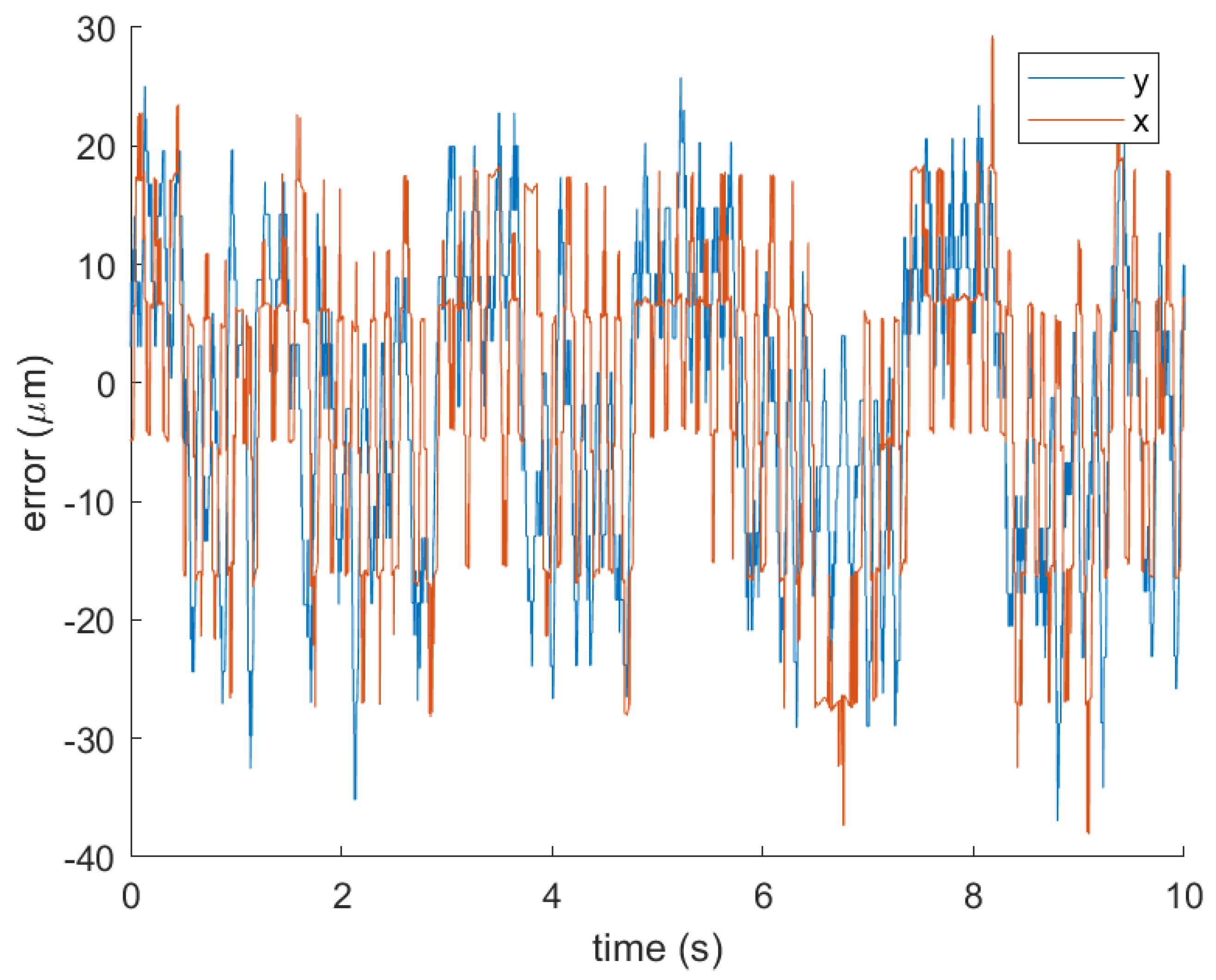
The error at steady-state is shown in
Figure 27 with the RMS error values provided in
Table 5. The periodic movement is caused by the correlation between the rotation and translational degrees of freedom. This is expected because the dummy wafer is not perfectly round. It must be noted that less rotation was observed during tracking than under steady-state.
7. Conclusions
The push for thinner and larger wafers has substantially increased the need for contactless handling of the substrates. The Flowerbed and other concepts were developed for this purpose using an air-bearing concept. This paper has presented an air-bearing contactless wafer handling system where the wafer’s position is sensed without any alterations to the wafer.
The performance of the inner loop has been improved from
to
by improving the controller. This is an improvement of almost 30 percent compared to previously published results [
13]. The inner loop creates a stable platform for the outer loop controller which controls the position of the wafer. External disturbances are handled in the inner loop, since the air does not transmit the vibrations from the floor.
With the use of three charge-coupled devices (CCD) the position of the wafer could be measured by detecting the edge of the wafer. This is done without any alteration of the wafer. The CCD sensors have a resolution of .
Due to the unforeseen lowering of the pneumatic gain than attained in previous studies, the bandwidth for control has not been improved. However, the wafer has been controlled using the new sensor’s design, resulting in a bandwidth of . The wafer can be positioned with a high accuracy of RMS, which is under 3 resolution counts of the sensor. This showcases the high precision positioning capability of the Flowerbed.
Further improvement of the inner loop could be achieved without redesign of the actuator. This improvement can be made by laminating the mover such that the effect from the eddy currents is removed. If lamination is not an option switching to flux feedback could remove the effect from the eddy currents, which are lowering the phase and thus the bandwidth. Additionally, decoupling filters could be used to improve the closed-loop sensitivity function of the inner loop. However, even in the current state the inner loop is no longer limiting the performance of the outer loop.
The resolution of the CCD could be improved to sub-micrometre resolution using sub-pixel interpolation techniques. Additionally, using improved data acquisition hardware it is possible to increase the sampling frequency of the current CCD from to .
Author Contributions
Conceptualization, all; methodology, R.H., N.S. and S.H.H.; software, R.H. and N.S.; validation, R.H., N.S., S.H.H. and R.A.J.v.O.; investigation, R.H.; writing—original draft preparation, R.H. and N.S.; writing—review and editing, all; supervision, R.A.J.v.O. All authors have read and agreed to the published version of the manuscript.
Funding
This research received no external funding.
Conflicts of Interest
The authors declare no conflict of interest.
References
- Fraunhofer ISE. Photovoltaics Report; Fraunhofer ISE: Freiburg, Germany, 2018. [Google Scholar]
- Carey, S.; Knotter, D.M.; Ooms, E.; Boersma, J.; van der Sar, E.; Cop, R.; Gerritzen, W.; van Zadelhoff, H.; Bouma, H. Yield Impact of Backside Metal-Ion Contamination. In Solid State Phenomena; Trans Tech Publications: Stafa-Zurich, Switzerland, 2012; Volume 187. [Google Scholar]
- Wesselingh, J. Contactless Positioning Using an Active Air Film. Ph.D. Thesis, Delft University of Technology, Delft, The Netherlands, 2011. Available online: https://repository.tudelft.nl/islandora/object/uuid%3A4f90d3b0-1698-4885-b4b4-bdec9d886893 (accessed on 17 August 2021).
- Vuong, P.H. Air-Based Contactless Actuation System for Thin Substrates. Ph.D. Thesis, Delft University of Technology, Delft, The Netherlands, 2016. Available online: https://repository.tudelft.nl/islandora/object/uuid%3A2d375f1b-3857-4c03-87e8-cb0fc45f3f13 (accessed on 17 August 2021).
- Verbruggen, N. Air-Based Contactless Positioning of Thing Substrates. Master’s Thesis, Delft University of Technology, Delft, The Netherlands, 2018. Available online: https://repository.tudelft.nl/islandora/object/uuid%3A42b0d71c-3055-41a8-8234-5acc8319f378 (accessed on 17 August 2021).
- Vagher, E.P. Contactless Passive Transport of Thin Solar Cells. Master’s Thesis, Delft University of Technology, Delft, The Netherlands, 2016. Available online: https://repository.tudelft.nl/islandora/object/uuid%3A1386cbd2-eca4-44a1-9dce-b8ec2083176b (accessed on 17 August 2021).
- Snieder, J. Development of an Air-Based Contactless Transport Demonstrator. Master’s thesis, Delft University of Technology, Delft, The Netherlands, 2017. Available online: https://repository.tudelft.nl/islandora/object/uuid%3A870adc6e-2f78-468c-a6c2-079eaec49226 (accessed on 17 August 2021).
- Voorrips, Y. The Design of a Distributed Sensing System for Contactless Substrate Transport. Master’s Thesis, Delft University of Technology, Delft, The Netherlands, 2017. Available online: https://repository.tudelft.nl/islandora/object/uuid%3A97c923e7-09d3-439b-87f2-e88d786d71b5 (accessed on 17 August 2021).
- Laurent, G.J.; Hyungpil, M. A survey of non-prehensile pneumatic manipulation surfaces: Principles, models and control. Intell. Serv. Robot. 2015, 8, 151–163. [Google Scholar] [CrossRef] [Green Version]
- Spaan-Burke, T.M.; van Dam, T.; Overschie, P.; Spaan, H.A. Contactless Shape Manipulation of Thin Substrates Using Air Bearing Table. In Proceedings of the 2017 ASPE Annual Meeting, Charlotte, NC, USA, 29 October–3 November 2017. [Google Scholar]
- Kim, J.-H. Design of the Air Pressure Pick-up Head for Non-Contact Wafer Gripper. J. Korean Soc. Manuf. Technol. Eng. 2012, 21, 401–407. [Google Scholar]
- Reinhart, G.; Heinz, M.; Stock, J.; Zimmermann, J.; Schilp, M.; Zitzmann, A.; Hellwig, J. Non-contact handling and transportation for substrates and microassembly using ultrasound-air-film-technology. In Proceedings of the 2011 IEEE/SEMI Advanced Semiconductor Manufacturing Conference, Saratoga Springs, NY, USA, 16–18 May 2011. [Google Scholar]
- Jansen, R. Actuation System for the FLowerbed. Master’s Thesis, Delft University of Technology, Delft, The Netherlands, 2018. Available online: https://repository.tudelft.nl/islandora/object/uuid%3Ab4a3a5da-c512-40ed-b631-cf2d6e638ce6 (accessed on 17 August 2021).
- Krijnen, M.E. Control System Design for a Contactless Actuation System. Master’s Thesis, Delft University of Technology, Delft, The Netherlands, 2016. Available online: https://repository.tudelft.nl/islandora/object/uuid%3Abef72c5e-7ca1-41eb-85ba-fc6fc59a6ce2 (accessed on 17 August 2021).
- Krijnen, M.E.; van Ostayen, R.A.; HosseinNia, H. The application of fractional order control for an air-based contactless actuation system. ISA Trans. 2018, 82, 172–183. [Google Scholar] [CrossRef] [PubMed] [Green Version]
- Katalenic, A. Control of Reluctance Actuators for High-Precision Positioning. Ph.D. Thesis, Technische Universiteit Eindhoven, Eindhoven, The Netherlands, 2013. [Google Scholar]
- Li, C.-M.; Xu, G.-S. Sub-pixel Edge Detection Based on Polynomial Fitting for Line-Matrix CCD Image. In Proceedings of the 2009 Second International Conference on Information and Computing Science, Manchester, UK, 21–22 May 2009; pp. 262–264. [Google Scholar] [CrossRef]
- Xu, G.-S. Linear Array CCD Image Sub-pixel Edge Detection Based on Wavelet Transform. In Proceedings of the 2009 Second International Conference on Information and Computing Science, Manchester, UK, 21–22 May 2009; pp. 204–206. [Google Scholar] [CrossRef]
- Fischer, J.; Pribula, O. Precise subpixel position measurement with linear interpolation of CMOS sensor image data. In Proceedings of the 6th IEEE International Conference on Intelligent Data Acquisition and Advanced Computing Systems, Prague, Czech Republic, 15–17 September 2011; pp. 500–504. [Google Scholar] [CrossRef]
- Hagara, M.; Kulla, O. Edge detection with sub-pixel accuracy based on approximation of edge with Erf function. Radioengineering 2011, 20, 516–524. [Google Scholar]
- Jan, F.; Tomas, R. Simple methods of edge position measurement using shadow projected on CCD sensor. Meas. Sci. Rev. 2003, 3, 37–40. [Google Scholar]
Figure 1.
Working principle of the first generation. (
a) Shows the cross-section of an actuator cell. (
b) Top view. (
c) The pressure variation demonstrator. For reference, the size of 6 × 6 actuator array in the centre of the image is
×
[
3,
13].
Figure 1.
Working principle of the first generation. (
a) Shows the cross-section of an actuator cell. (
b) Top view. (
c) The pressure variation demonstrator. For reference, the size of 6 × 6 actuator array in the centre of the image is
×
[
3,
13].
Figure 2.
The tilting surface concept, the surfaces are titled by bending the shafts [
4].
Figure 2.
The tilting surface concept, the surfaces are titled by bending the shafts [
4].
Figure 3.
Schematic of the second generation contactless actuator, showing the flow of air through the system, for a displacement
d of the movable plate [
13].
Figure 3.
Schematic of the second generation contactless actuator, showing the flow of air through the system, for a displacement
d of the movable plate [
13].
Figure 4.
A cross-section of the Flowerbed showing the fixed plate, flowers, and movable plate. Source: [
13].
Figure 4.
A cross-section of the Flowerbed showing the fixed plate, flowers, and movable plate. Source: [
13].
Figure 5.
Schematic of a single flower of the Flowerbed in (
a) neutral position and (
b) actuated position. The force on the wafer is visualized in the actuated position [
13].
Figure 5.
Schematic of a single flower of the Flowerbed in (
a) neutral position and (
b) actuated position. The force on the wafer is visualized in the actuated position [
13].
Figure 6.
Schematic of the flowerbed during (
a) translation and (
b) totation [
13].
Figure 6.
Schematic of the flowerbed during (
a) translation and (
b) totation [
13].
Figure 7.
The simulated and measured frequency response function of the Flowerbed with the reluctance actuator [
14].
Figure 7.
The simulated and measured frequency response function of the Flowerbed with the reluctance actuator [
14].
Figure 8.
Flapping modeshape of the actuators at 1080 Hz (measured) [
14].
Figure 8.
Flapping modeshape of the actuators at 1080 Hz (measured) [
14].
Figure 9.
Compliant mechanism design used to house the Lorentz actuators. Adapted from [
13].
Figure 9.
Compliant mechanism design used to house the Lorentz actuators. Adapted from [
13].
Figure 10.
Photograph of the Flowerbed with the compliant mechanism and Lorentz actuator design [
13].
Figure 10.
Photograph of the Flowerbed with the compliant mechanism and Lorentz actuator design [
13].
Figure 11.
Frequency response function from actuator force to actuator displacement, the phase is shifted upwards by 180 degrees since the position is measured in opposite direction to applied force.
Figure 11.
Frequency response function from actuator force to actuator displacement, the phase is shifted upwards by 180 degrees since the position is measured in opposite direction to applied force.
Figure 12.
The cross-coupled frequency response functions of the Flowerbed, the phase is shifted upwards by 180 degrees since the position is measured in opposite direction to applied force.
Figure 12.
The cross-coupled frequency response functions of the Flowerbed, the phase is shifted upwards by 180 degrees since the position is measured in opposite direction to applied force.
Figure 13.
Simulation showing the magnetic flux density (in
on the colorbar) and the eddy current density (arrows) [
13].
Figure 13.
Simulation showing the magnetic flux density (in
on the colorbar) and the eddy current density (arrows) [
13].
Figure 14.
Movable plate control strategy (ILC).
Figure 14.
Movable plate control strategy (ILC).
Figure 15.
Closed loop frequency response of the actuators, from actuator reference position to measured position.
Figure 15.
Closed loop frequency response of the actuators, from actuator reference position to measured position.
Figure 16.
Closed loop cross coupled frequency response of the actuators, from actuator reference position to measured position.
Figure 16.
Closed loop cross coupled frequency response of the actuators, from actuator reference position to measured position.
Figure 17.
Linear CCD sensor concept to measure the edge of a wafer.
Figure 17.
Linear CCD sensor concept to measure the edge of a wafer.
Figure 18.
Output of the CCD sensor. It shows the edge of the wafer. The edge is a curve over 10 pixels.
Figure 18.
Output of the CCD sensor. It shows the edge of the wafer. The edge is a curve over 10 pixels.
Figure 19.
A CCD sensor with 2 LEDs, showing the actual position of the wafer , the shadow created by the first led and second led .
Figure 19.
A CCD sensor with 2 LEDs, showing the actual position of the wafer , the shadow created by the first led and second led .
Figure 20.
Performance of CCD sensor analysed for linearity. RMS error value .
Figure 20.
Performance of CCD sensor analysed for linearity. RMS error value .
Figure 21.
The sensor placement in reference to the wafer to be controlled.
Figure 21.
The sensor placement in reference to the wafer to be controlled.
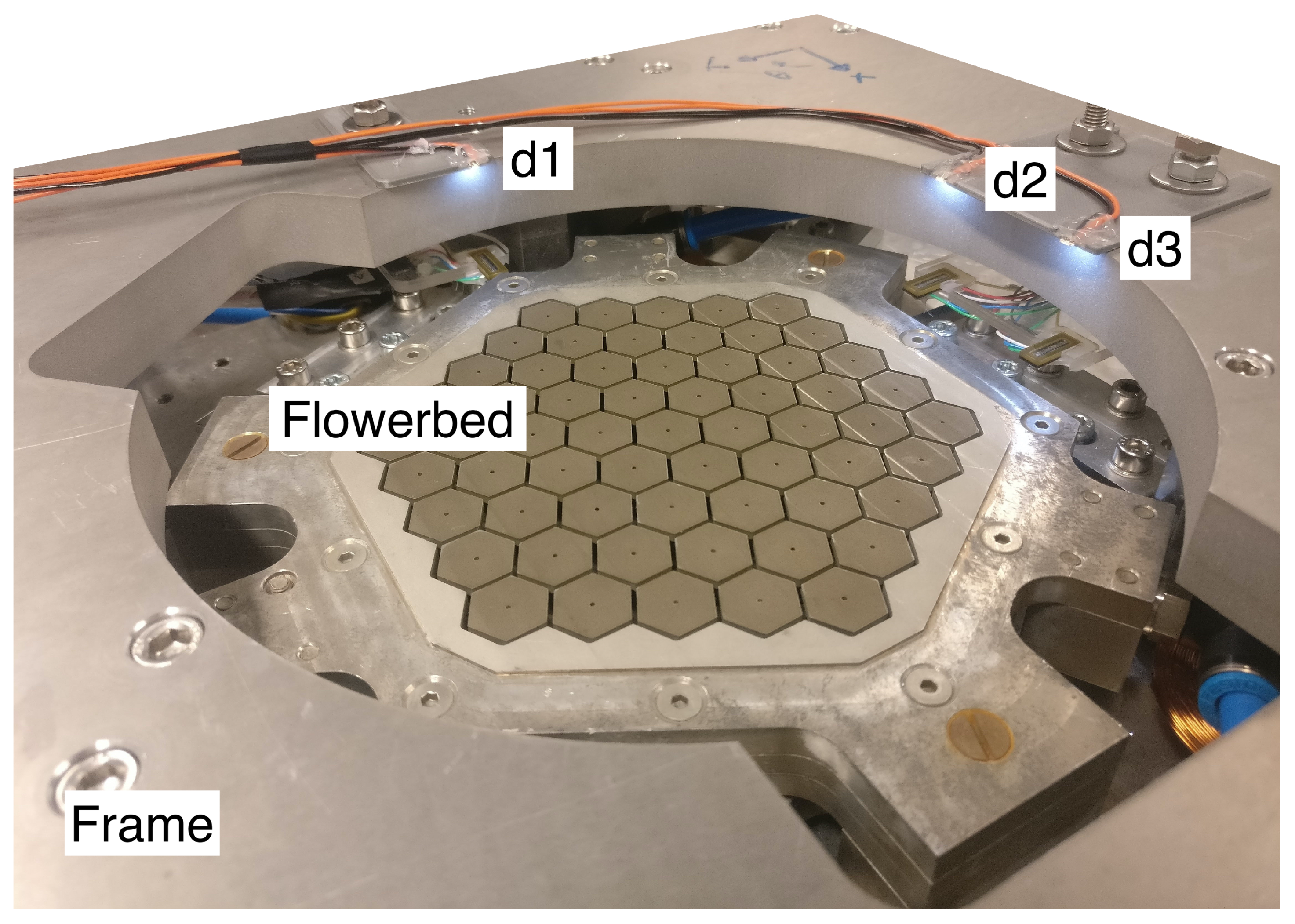
Figure 22.
Photograph of the Flowerbed system with the implemented contactless sensing system without the wafer. The position of the sensors has been annotated according to
Figure 21, and for reference, the diameter for the inscribed circle in each of the 61 hexagonal flowers is 14 mm.
Figure 22.
Photograph of the Flowerbed system with the implemented contactless sensing system without the wafer. The position of the sensors has been annotated according to
Figure 21, and for reference, the diameter for the inscribed circle in each of the 61 hexagonal flowers is 14 mm.
Figure 23.
The control strategy for the flowerbed.
Figure 23.
The control strategy for the flowerbed.
Figure 24.
The closed loop frequency response of the Flowerbed pressure control.
Figure 24.
The closed loop frequency response of the Flowerbed pressure control.
Figure 25.
The closed loop frequency response of the Flowerbed—T from the reference position to the measured position for the translations.
Figure 25.
The closed loop frequency response of the Flowerbed—T from the reference position to the measured position for the translations.
Figure 26.
Tracking response of the wafer.
Figure 26.
Tracking response of the wafer.
Figure 27.
The steady state error during control of the wafer in x and y.
Figure 27.
The steady state error during control of the wafer in x and y.
Table 1.
Flowerbed properties.
Table 1.
Flowerbed properties.
| Property | | Value |
|---|
| Translational stiffness | | |
| Rotational stiffness | | |
| Equivalent mass | | |
| Equivalent inertia | | |
| Translational eigenmode | | |
| Rotational eigenmode | | |
Table 2.
ILC-PID parameters.
Table 2.
ILC-PID parameters.
| Parameter | | Actuator 1 | Actuator 2 | Actuator 3 |
|---|
| K | N/m | 15.2 | 14.8 | 15.2 |
| | 10 | 10 | 10 |
| | 50 | 50 | 50 |
| | 2000 | 2000 | 2000 |
| | 2500 | 2500 | 2500 |
Table 3.
Pressure controller properties.
Table 3.
Pressure controller properties.
| Parameter | Pressure | Vacuum |
|---|
| 5000 | −1000 |
| 90 | 150 |
Table 4.
Outer loop controller properties.
Table 4.
Outer loop controller properties.
| Parameter | Translation | Rotation |
|---|
| 0.207 | 2.842 |
| 2.5 | 2.5 |
| 40 | 40 |
| 150 | 200 |
Table 5.
Wafer position control-steady state performance.
Table 5.
Wafer position control-steady state performance.
| DOF | RMS Error |
|---|
| x | |
| y | |
| Rz | |
| Publisher’s Note: MDPI stays neutral with regard to jurisdictional claims in published maps and institutional affiliations. |
© 2021 by the authors. Licensee MDPI, Basel, Switzerland. This article is an open access article distributed under the terms and conditions of the Creative Commons Attribution (CC BY) license (https://creativecommons.org/licenses/by/4.0/).


