Abstract
This work characterizes resistive switching and neuromorphic simulation of Pt/HfO2/TaN stack as an artificial synaptic device. A stable bipolar resistive switching operation is performed by repetitive DC sweep cycles. Furthermore, endurance (DC 100 cycles) and retention (5000 s) are demonstrated for reliable resistive operation. Low-resistance and high-resistance states follow the Ohmic conduction and Poole–Frenkel emission, respectively, which is verified through the fitting process. For practical operation, the set and reset processes are performed through pulses. Further, potentiation and depression are demonstrated for neuromorphic application. Finally, neuromorphic system simulation is performed through a neural network for pattern recognition accuracy of the Fashion Modified National Institute of Standards and Technology dataset.
1. Introduction
Resistive switching random access memory (RRAM) has attracted considerable attention in various applications such as storage memory [1,2,3,4,5,6,7,8,9,10,11,12,13,14,15,16], processing-in-memory (PIM) [17,18,19,20], and neuromorphic systems [21,22,23,24,25,26,27,28,29,30,31,32,33,34,35]. In the RRAM, the resistance value changes in a non-volatile and reversible manner depending on the magnitude and polarity of the applied voltage. However, a wide variety of switching characteristics is determined depending on the electrodes and dielectrics. The RRAM is divided into unipolar and bipolar types according to the switching polarity. Unipolar is commonly found in the dielectrics of NiO, HfO2, and TiO2, in which the set and reset processes occur in the same polarity [36,37,38]. In general, a high reset current due to Joule heating and a short endurance cycle are the major obstacles in the commercialization of the RRAM as a memory device. In contrast, the set and reset processes of the bipolar type occur at different polarities, and switching is reported in many materials, such as metal oxides, metal nitrides, 2D materials, and organic materials [1,2]. In the case of metal oxides such as TaOx and HfO2, excellent memory characteristics in terms of endurance, retention, and variability have been reported [39,40]. Upon further subdividing the bipolar type, in the case of a metal with good diffusion, such as Ag or Cu, the metal ions can penetrate the dielectric and form a conducting filament with applied bias [41,42,43]. In contrast, in the case of an MIM RRAM composed of non-diffusion type metals such as TiN and TaN and a metal oxide such as HfO2, TaOx, and Al2O3, the resistance value can be reversibly changed by the change in the oxygen vacancies inside the dielectric [44,45].
The RRAM has been developed and researched for a long time to develop a high-density memory [46]. However, the RRAM still needs to be improved to compete for reliable operation of phase-change random access memory in a cross-point structure [47] and the ultra-high-density NAND flash in a three-dimensional vertical structure [48]. The RRAM has recently been studied as an artificial synaptic device for neuromorphic systems owing to its excellent controllable multi-level cells, endurance, and low power consumption [1,2,3,4,5,6,7,8,9,10,11,12,13,14,15,16]. In the human brain, more than 100 billion neurons send signals to and receive signals from other neurons through connections called synapses, processing and storing information instantly. With approximately 100 billion neurons, more than 100 trillion synapses are connected in parallel; therefore, memory, computation, reasoning, and learning can be performed simultaneously with very low power [49]. The synapses convert chemical signals into electrical signals and then back into chemical signals. The neuromorphic system imitates the unique characteristics of synaptic plasticities—a phenomenon in which the contents repeatedly learned in the brain are remembered for a long time, and the contents learned in a short period are quickly forgotten. This process can be emulated by memory functions in the RRAM. The neuromorphic system is attracting attention as one of the artificial intelligence technologies because it can process large-scale parallel operations with low energy.
In this work, we characterize resistive switching, including the set and reset process, endurance, and retention by DC sweep of a Pt/HfO2/TaN device. The conduction mechanisms of the low-resistance state (LRS) and high-resistance state (HRS) are also discussed. Moreover, multi-level operation by the pulse for the set and reset processes is demonstrated. We demonstrate the potentiation and depression for the artificial synapse of the neuromorphic systems. Finally, a neural network system including the device conductance update is constructed to obtain the Modified National Institute of Standards and Technology dataset (MNIST) pattern recognition rate.
2. Materials and Methods
The Pt/HfO2/TaN devices were fabricated through the following process. A 100 nm thick TaN bottom electrode was deposited on a 300 nm thick SiO2 (dry oxidation)/Si wafer by DC sputtering. A HfO2 film of thickness 5 nm was deposited through atomic layer deposition (ALD) at a stage temperature of 260 °C. The sequence recipe of the ALD HfO2 film is: TDMAHf (0.5 s)–N2 purge (6 s)–H2O (0.5 s)–N2 purge (20 s) for a total of 54 cycles. A 100-nm-thick Pt top electrode was deposited via the shadow mask containing a circular pattern of diameter 100 μm. A Keithley 4200-SCS semiconductor parameter analyzer (Keithley Instrumnets, Cleveland, OH, USA) and a 4225-PMU pulse measurement (Keithley Instrumnets, Cleveland, OH, USA) unit in the probe station were used to measure the electrical characteristics using the DC sweep mode and transient features. A bias was applied to Pt and the top electrode and TiN bottom electrode were grounded. Further, an X-ray photoelectron spectroscopy (XPS) surface analysis was conducted using a Nexsa photoelectron spectrometer (Thermo Fisher Scientific, Waltham, MA, USA) with a microfocus monochromatic X-ray source (Al-Kα (1486.6 eV)), a sputter source (Ar+), an ion energy of 2 kV, and an X-ray beam size of 400 µm.
3. Results and Discussion
Figure 1a,b shows the XPS spectra of Hf 4f and O 1s of the surface of the HfO2 film. Two local peaks at 18.48 eV and 20.08 eV corresponding to Hf 4f7/2 and Hf 4f5/2 (Figure 1a), respectively, were observed [50], in addition to the two distinctive peaks for lattice oxygen and defect oxygen at 531.72 eV and 533.3 eV, respectively (Figure 1b). Defect oxygen indicates the oxygen vacancies initially existing in the HfO2 film [51], indicating that the HfO2 film deposited by XPS exhibits non-stoichiometry.
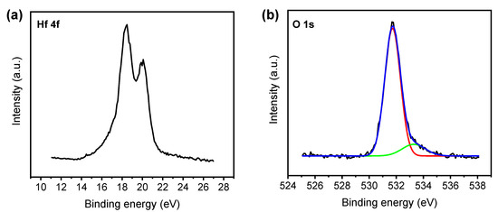
Figure 1.
XPS spectra of the HfO2 film on Si substrate: (a) Hf 4f and (b) O 1s.
Figure 2a shows the I–V curves, including the forming, set, and reset processes for the Pt/HfO2/TaN device. At approximately −2 V, the device is activated with a compliance current (CC) of 1 mA for resistive switching by the forming process. The initial resistance is 64.3 MΩ at −0.5 V, which is higher than an HRS resistance (9.51 kΩ). This is because the initial state has a lower defect compared to the HRS. The set process that converts the HRS to LRS in the device starts at approximately −0.8 V. The current jumps sharply at approximately 60 μA, and then the current starts to increase slowly at approximately 500 μA due to self-compliance. The self-compliance behavior is more clearly observed in the linear scale in Figure 2b.
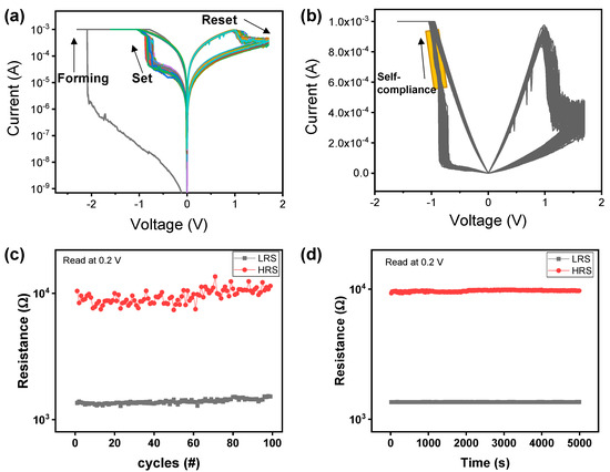
Figure 2.
Basic electrical measurement of the Pt/HfO2/TaN device for the memory device characteristics. I–V curves include the forming, set, and reset processes in (a) log scale and (b) linear scale. (c) endurance and (d) retention.
The decrease in the resistance during the set process can be explained by the increase in the oxygen vacancies in the HfO2 dielectric. The self-compliance current could be attributed to a TaON layer between the HfO2 and TaN layers. The TaON layer acting as a series resistance can be increased during the set process because of the oxidation of TaN [52]. In contrast, the reset process that converts the devices from the LRS to HRS occurs at the opposite polarity. The current abruptly decreases at approximately 1 V, and then the reset is completed through a gradual transition. The reset process can be explained by recombining the oxygen and oxygen vacancies, leading to an increase in the resistance. It is noted that the set and reset processes at opposite polarities do not exhibit good resistive switching (not shown here). This is because the oxygen exchange is more favorable for resistive switching when a positive bias is applied on the TaN electrode rather than the Pt electrode. Figure 2c shows the DC endurance cycles of the Pt/HfO2/TaN device in which the read voltage is 0.2 V for the LRS and HRS resistance values. The HRS controlled by the reset process has more considerable variations than the LRS controlled by the CC during the 100 cycles. Figure 2d shows the retention test for 5000 s in the LRS and HRS. The results confirmed the solid non-volatile properties of the Pt/HfO2/TaN device.
Next, we study the conduction mechanism of the Pt/HfO2/TaN device. Figure 3a shows a typical I–V curve for the fitting process. In the LRS, Ohmic conduction occurs from 0 V to 0.3 V. It is confirmed through log–log fitting with a slope of 1, as shown in Figure 3b. Ohmic conduction of the Pt/HfO2/TaN device indicates that the conducting filament composed of oxygen vacancies inside the HfO2 dielectric is connected between the top and bottom electrodes. However, in the region where the voltage is greater than 0.3 V, the slope of the I–V curve becomes greater than 1. Slopes greater than 1 at higher voltages may follow the space charge limited current mechanism [53]. In contrast, the HRS curve between 0.11 V and 1.22 V follows the relationship of ln(I/V)~sqrt(V) for the Poole–Frenkel emission, as shown in Figure 3c. The Poole–Frenkel current density is
where J is the current density, E is the electric field, q is the elementary charge, is the voltage barrier under zero electric fields, is dielectric constant, and kB is the Boltzmann constant [53,54]. When the voltage strengthens the electric field inside the dielectric, conduction proceeds as the electrons pass through the inner trap in the dielectric and pass over the conduction band. Similar results were reported in the different stacks of the Pt/TaOx/TiN devices [55]. Next, we demonstrate the multiple states in the pulse transient features of the Pt/TaOx/TaN device. Figure 4a shows the typical transient characteristics, including voltage and current with time for the set process. A voltage of −0.9 V is applied on the Pt/TaOx/TaN device for 1 ms. Only the current values are extracted to observe the multi-level states when a continuous pulse is applied, as shown in Figure 4b. It can be observed that the current level gradually increased when the set pulses of the same magnitude are continuously applied three times. In contrast, the pulse with a voltage of 1.1 V was applied on the devices, and the current decreased for the reset process, as shown in Figure 4c,d. Moreover, we demonstrate the potentiation and depression characteristics by applying 50 repeated pulses (Figure 5). However, there are some opposing points—the conductance generally increases when the set voltage is applied and decreases when the reset voltage is applied.

Figure 3.
(a) Fitting process of the I–V curve in the linear scale for the conduction mechanism. (b) Log–log scale in the LRS. (c) Ln (I/V) versus sqrt (V) in the HRS.
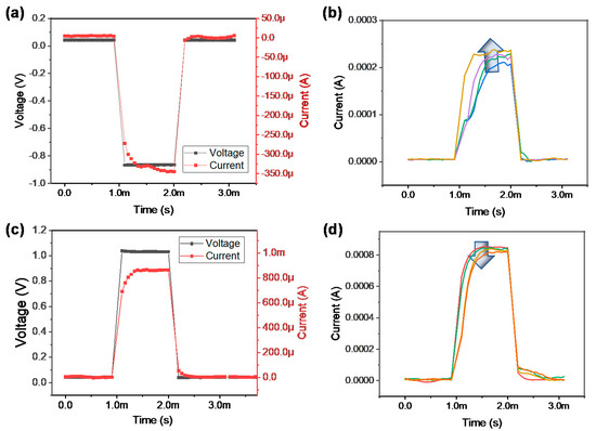
Figure 4.
Pulse transient characteristics: (a) set process and (b) current increase by identical set pulses, (c) reset process and (d) current decrease by identical reset pulses.
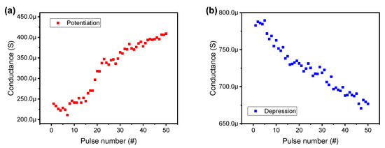
Figure 5.
(a) Potentiation and (b) depression by 50 identical set and reset pulses.
Finally, we calculate the accuracy of Fashion MNIST recognition by constructing a neural network (784 × 16 × 10), as shown in Figure 6a. Based on the measured conductance of the Pt/TaOx/TaN device, a pattern recognition test was simulated. To classify the image patterns of the Fashion MNIST dataset, first, 28 × 28 pixel images are rearranged in a one-dimensional array (784 × 1), and the pixel image exhibits values from 0 to 1 for 784 input neurons. The input layer nodes are fully connected to the 16 hidden layers that are fully connected to the 10 output neurons corresponding to the 10 classes of training and test images. The neurons of each layer are fully connected with the artificial synapse devices, which have quantized weight values. The imaginary cross-point array can perform a vector-matrix multiplication operation to update the synapse weight. Figure 6b shows the accuracy as a function of the epoch in which the accuracy at the 20th epoch is 89.07%.
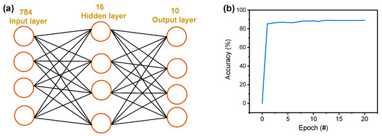
Figure 6.
(a) Two-layered neural network configuration. (b) Accuracy as a function of the epoch.
4. Conclusions
In summary, in this study, resistive switching behaviors were characterized by DC sweep and pulse operation. XPS analysis provided the chemical and material information of an HfO2/TaN stack. Further, stable bipolar resistive switching was achieved by the DC endurance cycle, and solid non-volatile memory properties were verified by the retention test. Then, multi-level states were obtained for the set and reset processes by pulse operation. Finally, the potentiation and depression were emulated by identical pulse schemes, and the pattern recognition accuracy of MNIST was performed by neural network simulation.
Author Contributions
H.R. and H.J. conducted the electrical measurements. H.R. wrote the manuscript; K.L. vilified the simulation work. S.K. designed the experiment and supervised the study. All authors have read and agreed to the published version of the manuscript.
Funding
This work was supported by the Korea Institute of Energy Technology Evaluation and Planning (KETEP) and the Ministry of Trade, Industry and Energy (MOTIE) of the Republic of Korea (No. 20194030202320) and by a National Research Foundation of Korea (NRF) grant funded by the Ministry of Science and ICT (2021K1A3A1A49098073).
Institutional Review Board Statement
Not applicable.
Informed Consent Statement
Not applicable.
Data Availability Statement
Not applicable.
Conflicts of Interest
The authors declare no conflict of interest.
References
- Lanza, M.; Wong, H.-S.P.; Pop, E.; Ielmini, D.; Strukov, D.; Regan, B.C.; Larcher, L.; Villena, M.A.; Yang, J.J.; Goux, L.; et al. Recommended Methods to Study Resistive Switching Devices. Adv. Electron. Mater. 2019, 5, 1800143. [Google Scholar] [CrossRef] [Green Version]
- Pan, F.; Gao, S.; Chen, C.; Song, C.; Zeng, F. Recent progress in resistive random access memories: Materials, switching mechanisms, and performance. Mater. Sci. Eng. R Rep. 2014, 83, 1–59. [Google Scholar] [CrossRef]
- Waser, R.; Dittmann, R.; Staikov, G.; Szot, K. Redox-Based Resistive Switching Memories—Nanoionic Mechanisms, Prospects, and Challenges. Adv. Mater. 2009, 21, 2632–2663. [Google Scholar] [CrossRef]
- Mikhaylov, A.; Belov, A.; Korolev, D.; Antonov, I.; Kotomina, V.; Kotina, A.; Gryaznov, E.; Sharapov, A.; Koryazhkina, M.; Kryukov, R.; et al. Multilayer Metal-Oxide Memristive Device with Stabilized Resistive Switching. Adv. Mater. Technol. 2020, 5, 1900607. [Google Scholar] [CrossRef]
- Choi, J.; Kim, S. Improved Stability and Controllability in ZrN-Based Resistive Memory Device by Inserting TiO2 Layer. Micromachines 2020, 11, 905. [Google Scholar] [CrossRef]
- Ryu, H.; Choi, J.; Kim, S. Voltage Amplitude-Controlled Synaptic Plasticity from Complementary Resistive Switching in Alloying HfOx with AlOx-Based RRAM. Metals 2020, 10, 1410. [Google Scholar] [CrossRef]
- Ryu, H.; Kim, S. Improved Pulse-Controlled Conductance Adjustment in Trilayer Resistors by Suppressing Current Overshoot. Nanomaterials 2020, 10, 2462. [Google Scholar] [CrossRef]
- Chandrasekaran, S.; Simanjuntak, F.M.; Saminathan, R.; Panda, D.; Tseng, T.-Y. Improving linearity by introducing Al in HfO2 as a memristor synapse device. Nanotechnology 2019, 30, 445205. [Google Scholar] [CrossRef]
- Su, T.-H.; Lee, K.-J.; Wang, L.-W.; Chang, Y.-C.; Wang, Y.-H. Resistive Switching Behavior of Magnesium Zirconia Nickel Nanorods. Materials 2020, 13, 2755. [Google Scholar] [CrossRef] [PubMed]
- Choi, J.; Kim, S. Nonlinear Characteristics of Complementary Resistive Switching in HfAlOx-Based Memristor for High-Density Cross-Point Array Structure. Coatings 2020, 10, 765. [Google Scholar] [CrossRef]
- Ismail, M.; Kim, S. Negative differential resistance effect and dual bipolar resistive switching properties in a transparent Ce-based devices with opposite forming polarity. Appl. Surf. Sci. 2020, 530, 147284. [Google Scholar] [CrossRef]
- Simanjuntak, F.M.; Ohno, T.; Samukawa, S. Film-Nanostructure-Controlled Inerasable-to-Erasable Switching Transition in ZnO-Based Transparent Memristor Devices: Sputtering-Pressure Dependency. ACS Appl. Electron. Mater. 2019, 1, 2183–2189. [Google Scholar] [CrossRef]
- Zhang, Z.; Wang, F.; Hu, K.; She, Y.; Song, S.; Song, Z.; Zhang, K. Improvement of Resistive Switching Performance in Sulfur-Doped HfOx-Based RRAM. Materials 2021, 14, 3330. [Google Scholar] [CrossRef]
- Yen, T.-J.; Chin, A.; Gritsenko, V. Improved Device Distribution in High-Performance SiNx Resistive Random Access Memory via Arsenic Ion Implantation. Nanomaterials 2021, 11, 1401. [Google Scholar] [CrossRef] [PubMed]
- Chen, K.-H.; Kao, M.-C.; Huang, S.-J.; Li, J.-Z. Bipolar Switching Properties of Neodymium Oxide RRAM Devices Using by a Low Temperature Improvement Method. Materials 2017, 10, 1415. [Google Scholar] [CrossRef] [Green Version]
- Lee, K.-J.; Chang, Y.-C.; Lee, C.-J.; Wang, L.-W.; Wang, Y.-H. 1T1R Nonvolatile Memory with Al/TiO2/Au and Sol-Gel-Processed Insulator for Barium Zirconate Nickelate Gate in Pentacene Thin Film Transistor. Materials 2017, 10, 1408. [Google Scholar] [CrossRef] [Green Version]
- Vasileiadis, N.; Ntinas, V.; Sirakoulis, G.C.; Dimitrakis, P. In-Memory-Computing Realization with a Photodiode/Memristor Based Vision Sensor. Materials 2021, 14, 5223. [Google Scholar] [CrossRef]
- Ielmini, D.; Wong, H.-S.P. In-memory computing with resistive switching devices. Nat. Electron. 2018, 1, 333–343. [Google Scholar] [CrossRef]
- Pérez, E.; Pérez-Ávila, A.; Romero-Zaliz, R.; Mahadevaiah, M.; Quesada, E.P.-B.; Roldán, J.; Jiménez-Molinos, F.; Wenger, C. Optimization of Multi-Level Operation in RRAM Arrays for In-Memory Computing. Electronics 2021, 10, 1084. [Google Scholar] [CrossRef]
- Pedretti, G.; Ielmini, D. In-Memory Computing with Resistive Memory Circuits: Status and Outlook. Electronics 2021, 10, 1063. [Google Scholar] [CrossRef]
- Cho, H.; Kim, S. Short-Term Memory Dynamics of TiN/Ti/TiO2/SiOx/Si Resistive Random Access Memory. Nanomaterials 2020, 10, 1821. [Google Scholar] [CrossRef]
- Shen, Z.; Zhao, C.; Qi, Y.; Xu, W.; Liu, Y.; Mitrovic, I.Z.; Yang, L.; Zhao, C. Advances of RRAM Devices: Resistive Switching Mechanisms, Materials and Bionic Synaptic Application. Nanomaterials 2020, 10, 1437. [Google Scholar] [CrossRef]
- Maikap, S.; Banergee, W. In Quest of Nonfilamentary Switching: A Synergistic Approach of Dual Nanostructure Engineering to Improve the Variability and Reliability of Resistive Random-Access-Memory Devices. Adv. Electron. Mater. 2020, 6, 2000209. [Google Scholar] [CrossRef]
- Ryu, H.; Kim, S. Self-Rectifying Resistive Switching and Short-Term Memory Characteristics in Pt/HfO2/TaOx/TiN Artificial Synaptic Device. Nanomaterials 2020, 10, 2159. [Google Scholar] [CrossRef] [PubMed]
- Surazhevsky, I.; Demin, V.; Ilyasov, A.; Emelyanov, A.; Nikiruy, K.; Rylkov, V.; Shchanikov, S.; Bordanov, I.; Gerasimova, S.; Guseinov, D.; et al. Noise-assisted persistence and recovery of memory state in a memristive spiking neuromorphic network. Chaos Solitons Fractals 2021, 146, 110890. [Google Scholar] [CrossRef]
- Simanjuntak, F.M.; Ohno, T.; Chandresekaran, S.; Samukawa, S. Neutral oxygen irradiation enhanced forming-less ZnO-based transparent analog memristor devices for neuromorphic computing applications. Nanoechnology 2020, 31, 26LT01. [Google Scholar] [CrossRef]
- Ryu, H.; Kim, S. Implementation of a reservoir computing system using the short-term effects of Pt/HfO2/TaOx/TiN memristors with self-rectification. Chaos Soliton. Fract. 2021, 150, 111223. [Google Scholar] [CrossRef]
- Wang, I.T.; Chang, C.C.; Chiu, L.W.; Chou, T.; Hou, T.H. 3D Ta/TaOx/TiO2/Ti synaptic array and linearity tuning of weight update for hardware neural network applications. Nanotechnology 2016, 27, 365204. [Google Scholar] [CrossRef] [Green Version]
- Emelyanov, A.V.; Nikiruy, K.E.; Serenko, A.V.; Sitnikov, A.V.; Presnyakov, M.Y.; Rybka, R.B.; Sboev, A.G.; Rylkov, V.V.; Kashkarov, P.K.; Kovalchuk, M.V.; et al. Self-adaptive STDP-based learning of a spiking neuron with nanocomposite memristive weights. Nanotechnology 2020, 31, 045201. [Google Scholar] [CrossRef]
- Mikhaylov, A.; Pimashkin, A.; Pigareva, Y.; Gerasimova, S.; Gryaznov, E.; Shchanikov, S.; Zuev, A.; Talanov, M.; Lavrov, I.; Demin, V.; et al. Neurohybrid Memristive CMOS-Integrated Systems for Biosensors and Neuroprosthetics. Front. Neurosci. 2020, 14, 358. [Google Scholar] [CrossRef]
- Chen, L.; He, Z.-Y.; Wang, T.-Y.; Dai, Y.-W.; Zhu, H.; Sun, Q.-Q.; Zhang, D.W. CMOS Compatible Bio-Realistic Implementation with Ag/HfO2-Based Synaptic Nanoelectronics for Artificial Neuromorphic System. Electronics 2018, 7, 80. [Google Scholar] [CrossRef] [Green Version]
- Wang, Y.; Chen, X.; Shen, D.; Zhang, M.; Chen, X.; Chen, X.; Shao, W.; Gu, H.; Xu, J.; Hu, E.; et al. Artificial Neurons Based on Ag/V2C/W Threshold Switching Memristors. Nanomaterials 2021, 11, 2860. [Google Scholar] [CrossRef]
- Gerasimova, S.A.; Belov, A.I.; Korolev, D.S.; Guseinov, D.V.; Lebedeva, A.V.; Koryazhkina, M.N.; Mikhaylov, A.N.; Kazantsev, V.B.; Pisarchik, A.N. Stochastic Memristive Interface for Neural Signal Processing. Sensors 2021, 21, 5587. [Google Scholar] [CrossRef]
- Ryu, H.; Kim, S. Gradually Tunable Conductance in TiO2/Al2O3 Bilayer Resistors for Synaptic Device. Metals 2021, 11, 440. [Google Scholar] [CrossRef]
- Ryu, H.; Kim, S. Volatile Resistive Switching Characteristics of Pt/HfO2/TaOx/TiN Short-Term Memory Device. Metals 2021, 11, 1207. [Google Scholar] [CrossRef]
- Ielmini, D.; Nardi, F.; Cagli, C. Physical models of size-dependent nanofilament formation and rupture in NiO resistive switching memories. Nanotechnology 2011, 22, 254022. [Google Scholar] [CrossRef]
- Jeong, D.S.; Schroeder, H.; Waser, R. Coexistence of Bipolar and Unipolar Resistive Switching Behaviors in a Pt/TiO2/Pt Stack, Electrochem. Solid-State Lett. 2007, 10, G41. [Google Scholar] [CrossRef]
- Kang, J.; Park, I.S. Asymmetric Current Behavior on Unipolar Resistive Switching in Pt/HfO2/Pt Resistor with Symmetric Electrodes. IEEE Trans. Electron. Dev. 2016, 63, 2380. [Google Scholar] [CrossRef]
- Pérez, E.; Ossorio, Ó.G.; Dueñas, S.; Castán, H.; García, H.; Wenger, C. Programming Pulse Width Assessment for Reliable and Low-Energy Endurance Performance in Al:HfO2-Based RRAM Arrays. Electronics 2020, 9, 864. [Google Scholar] [CrossRef]
- Lee, M.J.; Lee, C.B.; Lee, D.; Lee, S.R.; Chang, M.; Hur, J.H.; Kim, Y.-B.; Kim, C.-J.; Seo, D.H.; Seo, S.; et al. A fast, high endurance and scalable non-volatile memory device made from asymmetric Ta2O5-x/TaO2-x bilayer structures. Nat. Mat. 2011, 10, 625–630. [Google Scholar] [CrossRef]
- Yang, J.; Ryu, H.; Kim, S. Resistive and synaptic properties modulation by electroforming polarity in CMOS-compatible Cu/HfO2/Si device. Chaos Solitons Fractals 2021, 145, 110783. [Google Scholar] [CrossRef]
- Ryu, H.; Kim, S. Irregular Resistive Switching Behaviors of Al2O3—Based Resistor with Cu Electrode. Metals 2021, 11, 653. [Google Scholar] [CrossRef]
- Lian, X.; Shen, X.; Fu, J.; Gao, Z.; Wan, X.; Liu, X.; Hu, E.; Xu, J.; Tong, Y. Electrical Properties and Biological Synaptic Simulation of Ag/MXene/SiO2/Pt RRAM Devices. Electronics 2020, 9, 2098. [Google Scholar] [CrossRef]
- Ryu, H.; Kim, S. Gradually Modified Conductance in the Self-Compliance Region of an Atomic-Layer-Deposited Pt/TiO2/HfAlOx/TiN RRAM Device. Metals 2021, 11, 1199. [Google Scholar] [CrossRef]
- Choi, S.Y.; Yang, M.K.; Kim, S.; Lee, J.-K. Fully room-temperature-fabricated TiN/TaOx/Pt nonvolatile memory devices. Phys. Status Solidi Rapid Res. Lett. 2010, 4, 359–361. [Google Scholar] [CrossRef]
- Salahuddin, S.; Ni, K.; Datta, S. The era of hyper-scaling in electronics. Nat. Electron. 2018, 1, 442–450. [Google Scholar] [CrossRef]
- Fong, S.W.; Neumann, C.M.; Wong, H.-S.P. Phase-Change Memory—Towards a Storage-Class Memory. IEEE Trans. Electron. Devices 2017, 64, 4374–4385. [Google Scholar] [CrossRef]
- Lee, G.; Hwang, S.; Yu, J.; Kim, H. Architecture and Process Integration Overview of 3D NAND Flash Technologies. Appl. Sci. 2021, 11, 6703. [Google Scholar] [CrossRef]
- Yang, J.J.; Strukov, D.B.; Stewart, D.R. Memristive devices for computing. Nat. Nanotechnol. 2013, 8, 13–24. [Google Scholar] [CrossRef]
- Liu, C.-F.; Tang, X.-G.; Wang, L.-Q.; Tang, H.; Jiang, Y.-P.; Liu, Q.-X.; Li, W.-H.; Tang, Z.-H. Resistive Switching Characteristics of HfO2 Thin Films on Mica Substrates Prepared by Sol-Gel Process. Nanomaterials 2019, 9, 1124. [Google Scholar] [CrossRef] [Green Version]
- Oh, I.-K.; Park, B.-E.; Seo, S.; Yeo, B.C.; Tanskanen, J.; Lee, H.-B.-R.; Kim, W.-H.; Kim, H. Comparative study of the growth characteristics and electrical properties of atomic-layer-deposited HfO2 films obtained from metal halide and amide precursors. J. Mater. Chem. C 2018, 6, 7367–7376. [Google Scholar] [CrossRef]
- Cheng, C.H.; Chen, P.C.; Wu, Y.H.; Yeh, F.S.; Chin, A. Long-Endurance Nanocrystal TiO2 Resistive Memory Using a TaON Buffer Layer. IEEE Electron. Dev. Lett. 2011, 32, 1749–1751. [Google Scholar] [CrossRef]
- Lim, E.W.; Ismail, R. Conduction Mechanism of Valence Change Resistive Switching Memory: A Survey. Electronics 2015, 4, 586–613. [Google Scholar] [CrossRef]
- Chang, Y.-F.; Fowler, B.; Chen, Y.-C.; Chen, Y.-T.; Wang, Y.; Xue, F.; Zhou, F.; Lee, J.C. Intrinsic SiOx-based unipolar resistive switching memory. II. Thermal effects on charge transport and characterization of multilevel programing. J. Appl. Phys. 2014, 116, 043709. [Google Scholar] [CrossRef]
- Jeon, H.; Park, J.; Jang, W.; Kim, H.; Kang, C.; Song, H.; Kim, H.; Seo, H.; Jeon, H. Stabilzed resistive switching behaviors of a Pt/TaOx/TiN RRAM under different oxygen contents. Phys. Status Solidi A 2014, 211, 2189–2194. [Google Scholar] [CrossRef]
Publisher’s Note: MDPI stays neutral with regard to jurisdictional claims in published maps and institutional affiliations. |
© 2021 by the authors. Licensee MDPI, Basel, Switzerland. This article is an open access article distributed under the terms and conditions of the Creative Commons Attribution (CC BY) license (https://creativecommons.org/licenses/by/4.0/).